Our official English website, www.x-mol.net, welcomes your
feedback! (Note: you will need to create a separate account there.)
Large‐Area Patterning of Metal Nanostructures by Dip‐Pen Nanodisplacement Lithography for Optical Applications
Small ( IF 13.0 ) Pub Date : 2017-09-20 , DOI: 10.1002/smll.201702003 Lina Chen 1 , Xiaoling Wei 1 , Xuechang Zhou 1 , Zhuang Xie 1, 2 , Kan Li 1 , Qifeng Ruan 3 , Chaojian Chen 1 , Jianfang Wang 3 , Chad A. Mirkin 2 , Zijian Zheng 1
Small ( IF 13.0 ) Pub Date : 2017-09-20 , DOI: 10.1002/smll.201702003 Lina Chen 1 , Xiaoling Wei 1 , Xuechang Zhou 1 , Zhuang Xie 1, 2 , Kan Li 1 , Qifeng Ruan 3 , Chaojian Chen 1 , Jianfang Wang 3 , Chad A. Mirkin 2 , Zijian Zheng 1
Affiliation
|
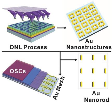
Au nanostructures are remarkably important in a wide variety of fields for decades. The fabrication of Au nanostructures typically requires time‐consuming and expensive electron‐beam lithography (EBL) that operates in vacuum. To address this challenge, this paper reports the development of massive dip‐pen nanodisplacement lithography (DNL) as a desktop fabrication tool, which allows high‐throughput and rational design of arbitrary Au nanopatterns in ambient condition. Large‐area (1 cm2) and uniform (<10% variation) Au nanostructures as small as 70 nm are readily fabricated, with a throughput 100‐fold higher than that of conventional EBL. As a proof‐of‐concept of the applications in the opitcal field, we fabricate discrete Au nanorod arrays that show significant plasmonic resonance in the visible range, and interconnected Au nanomeshes that are used for transparent conductive electrode of solar cells.
中文翻译:

蘸笔纳米位移光刻技术在金属纳米结构上进行大面积构图,以用于光学应用
几十年来,金纳米结构在许多领域都非常重要。金纳米结构的制造通常需要耗时且昂贵的真空电子束光刻(EBL)。为了应对这一挑战,本文报道了大规模浸笔式纳米位移光刻技术(DNL)作为台式机制造工具的发展,该工具可以在环境条件下对任意Au纳米图案进行高通量和合理的设计。大面积(1 cm 2)和均匀(小于10%的变化)的Au纳米结构很容易制造出来,小至70 nm,其吞吐率是传统EBL的100倍。作为光电领域应用的概念验证,我们制造了分立的Au纳米棒阵列,该阵列在可见光范围内显示出明显的等离子体共振,并互连了用于太阳能电池透明导电电极的Au纳米网。
更新日期:2017-09-20
中文翻译:
蘸笔纳米位移光刻技术在金属纳米结构上进行大面积构图,以用于光学应用
几十年来,金纳米结构在许多领域都非常重要。金纳米结构的制造通常需要耗时且昂贵的真空电子束光刻(EBL)。为了应对这一挑战,本文报道了大规模浸笔式纳米位移光刻技术(DNL)作为台式机制造工具的发展,该工具可以在环境条件下对任意Au纳米图案进行高通量和合理的设计。大面积(1 cm 2)和均匀(小于10%的变化)的Au纳米结构很容易制造出来,小至70 nm,其吞吐率是传统EBL的100倍。作为光电领域应用的概念验证,我们制造了分立的Au纳米棒阵列,该阵列在可见光范围内显示出明显的等离子体共振,并互连了用于太阳能电池透明导电电极的Au纳米网。


 京公网安备 11010802027423号