当前位置:
X-MOL 学术
›
Nano Lett.
›
论文详情
Our official English website, www.x-mol.net, welcomes your
feedback! (Note: you will need to create a separate account there.)
GaN Metalens for Pixel-Level Full-Color Routing at Visible Light
Nano Letters ( IF 9.6 ) Pub Date : 2017-09-18 00:00:00 , DOI: 10.1021/acs.nanolett.7b03135 Bo Han Chen,Pin Chieh Wu,Vin-Cent Su,Yi-Chieh Lai,Cheng Hung Chu,I Chen Lee,Jia-Wern Chen,Yu Han Chen,Yung-Chiang Lan,Chieh-Hsiung Kuan,Din Ping Tsai
Nano Letters ( IF 9.6 ) Pub Date : 2017-09-18 00:00:00 , DOI: 10.1021/acs.nanolett.7b03135 Bo Han Chen,Pin Chieh Wu,Vin-Cent Su,Yi-Chieh Lai,Cheng Hung Chu,I Chen Lee,Jia-Wern Chen,Yu Han Chen,Yung-Chiang Lan,Chieh-Hsiung Kuan,Din Ping Tsai
|
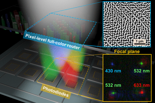
Metasurface-based components are known to be one of the promising candidates for developing flat optical systems. However, their low working efficiency highly limits the use of such flat components for feasible applications. Although the introduction of the metallic mirror has been demonstrated to successfully enhance the efficiency, it is still somehow limited for imaging and sensing applications because they are only available for devices operating in a reflection fashion. Here, we demonstrate three individual GaN-based metalenses working in a transmission window with extremely high operation efficiency at visible light (87%, 91.6%, and 50.6% for blue, green, and red light, respectively). For the proof of concept, a multiplex color router with dielectric metalens, which is capable of guiding individual primary colors into different spatial positions, is experimentally verified based on the design of out-of-plane focusing metalens. Our approach with low-cost, semiconductor fabrication compatibility and high working efficiency characteristics offers a way for establishing a complete set of flat optical components for a wide range of applications such as compact imaging sensors, optical spectroscopy, and high-resolution lithography, just named a few.
中文翻译:

GaN Metalens在可见光下实现像素级全彩布线
已知基于超表面的组件是开发平面光学系统的有前途的候选者之一。然而,它们的低工作效率极大地限制了将这种扁平部件用于可行的应用。尽管已经证明了引入金属镜可以成功提高效率,但是由于它们仅适用于以反射方式运行的设备,因此它在某种程度上仍受成像和传感应用的限制。在这里,我们演示了三个单独的基于GaN的金属传感器,它们在透射窗中在可见光下具有极高的工作效率(蓝光,绿光和红光分别为87%,91.6%和50.6%)。为了证明这一点,我们使用了具有介电金属元素的多路复用彩色路由器,基于平面外聚焦金属元素的设计,通过实验验证了这种颜色能够将各个原色引导到不同的空间位置。我们的方法具有低成本,半导体制造兼容性和高工作效率特性的特点,为建立广泛适用于紧凑型成像传感器,光谱学和高分辨率光刻等广泛应用的平面光学组件提供了一种方法。一些。
更新日期:2017-09-19
中文翻译:
GaN Metalens在可见光下实现像素级全彩布线
已知基于超表面的组件是开发平面光学系统的有前途的候选者之一。然而,它们的低工作效率极大地限制了将这种扁平部件用于可行的应用。尽管已经证明了引入金属镜可以成功提高效率,但是由于它们仅适用于以反射方式运行的设备,因此它在某种程度上仍受成像和传感应用的限制。在这里,我们演示了三个单独的基于GaN的金属传感器,它们在透射窗中在可见光下具有极高的工作效率(蓝光,绿光和红光分别为87%,91.6%和50.6%)。为了证明这一点,我们使用了具有介电金属元素的多路复用彩色路由器,基于平面外聚焦金属元素的设计,通过实验验证了这种颜色能够将各个原色引导到不同的空间位置。我们的方法具有低成本,半导体制造兼容性和高工作效率特性的特点,为建立广泛适用于紧凑型成像传感器,光谱学和高分辨率光刻等广泛应用的平面光学组件提供了一种方法。一些。


 京公网安备 11010802027423号