当前位置:
X-MOL 学术
›
Adv. Mater.
›
论文详情
Our official English website, www.x-mol.net, welcomes your
feedback! (Note: you will need to create a separate account there.)
Characterization of Edge Contact: Atomically Resolved Semiconductor–Metal Lateral Boundary in MoS2
Advanced Materials ( IF 27.4 ) Pub Date : 2017-09-18 , DOI: 10.1002/adma.201702931 Hyeokshin Kwon 1 , Kiyoung Lee 1 , Jinseong Heo 1 , Youngtek Oh 1 , Hyangsook Lee 1 , Samudrala Appalakondaiah 2 , Wonhee Ko 1 , Hyo Won Kim 1 , Jin-Wook Jung 1 , Hwansoo Suh 1 , Hongki Min 3 , Insu Jeon 1 , Euyheon Hwang 2 , Sungwoo Hwang 1
Advanced Materials ( IF 27.4 ) Pub Date : 2017-09-18 , DOI: 10.1002/adma.201702931 Hyeokshin Kwon 1 , Kiyoung Lee 1 , Jinseong Heo 1 , Youngtek Oh 1 , Hyangsook Lee 1 , Samudrala Appalakondaiah 2 , Wonhee Ko 1 , Hyo Won Kim 1 , Jin-Wook Jung 1 , Hwansoo Suh 1 , Hongki Min 3 , Insu Jeon 1 , Euyheon Hwang 2 , Sungwoo Hwang 1
Affiliation
|
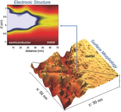
Despite recent efforts for the development of transition‐metal‐dichalcogenide‐based high‐performance thin‐film transistors, device performance has not improved much, mainly because of the high contact resistance at the interface between the 2D semiconductor and the metal electrode. Edge contact has been proposed for the fabrication of a high‐quality electrical contact; however, the complete electronic properties for the contact resistance have not been elucidated in detail. Using the scanning tunneling microscopy/spectroscopy and scanning transmission electron microscopy techniques, the edge contact, as well as the lateral boundary between the 2D semiconducting layer and the metalized interfacial layer, are investigated, and their electronic properties and the energy band profile across the boundary are shown. The results demonstrate a possible mechanism for the formation of an ohmic contact in homojunctions of the transition‐metal dichalcogenides semiconductor–metal layers and suggest a new device scheme utilizing the low‐resistance edge contact.
中文翻译:

边缘接触的表征:MoS2中的原子分辨半导体-金属横向边界
尽管最近在开发基于过渡金属二卤化氢的高性能薄膜晶体管方面做出了很多努力,但设备性能并未得到很大改善,这主要是由于2D半导体和金属电极之间的界面处的接触电阻很高。边缘接触已被提议用于制造高质量的电接触。但是,尚未详细说明接触电阻的完整电子性能。使用扫描隧道显微镜/光谱学和扫描透射电子显微镜技术,研究了2D半导体层和金属化界面层之间的边缘接触以及横向边界,并研究了它们的电子性质和跨边界的能带分布显示。
更新日期:2017-09-18
中文翻译:
边缘接触的表征:MoS2中的原子分辨半导体-金属横向边界
尽管最近在开发基于过渡金属二卤化氢的高性能薄膜晶体管方面做出了很多努力,但设备性能并未得到很大改善,这主要是由于2D半导体和金属电极之间的界面处的接触电阻很高。边缘接触已被提议用于制造高质量的电接触。但是,尚未详细说明接触电阻的完整电子性能。使用扫描隧道显微镜/光谱学和扫描透射电子显微镜技术,研究了2D半导体层和金属化界面层之间的边缘接触以及横向边界,并研究了它们的电子性质和跨边界的能带分布显示。


 京公网安备 11010802027423号