当前位置:
X-MOL 学术
›
CrystEngComm
›
论文详情
Our official English website, www.x-mol.net, welcomes your
feedback! (Note: you will need to create a separate account there.)
Growth of a void-free Cu2SnS3 thin film using a Cu/SnS2 precursor through an intermediate-temperature pre-annealing and sulfurization process
CrystEngComm ( IF 2.6 ) Pub Date : 2017-09-15 00:00:00 , DOI: 10.1039/c7ce01261f Young Min Ko 1, 2, 3, 4 , R. B. V. Chalapathy 4, 5, 6, 7, 8 , Liudmila Larina 1, 2, 3, 4 , Byung Tae Ahn 1, 2, 3, 4
CrystEngComm ( IF 2.6 ) Pub Date : 2017-09-15 00:00:00 , DOI: 10.1039/c7ce01261f Young Min Ko 1, 2, 3, 4 , R. B. V. Chalapathy 4, 5, 6, 7, 8 , Liudmila Larina 1, 2, 3, 4 , Byung Tae Ahn 1, 2, 3, 4
Affiliation
|
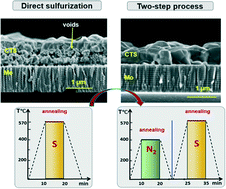
Ternary earth-abundant Cu2SnS3 (CTS) absorbers were synthesized from a Cu/SnS2 stacked precursor by direct annealing in a S atmosphere and by pre-annealing at lower temperature followed by sulfurization. The existing S within the chosen Cu/SnS2 precursor allows avoiding the interface voids commonly generated from a metal precursor. We found that direct annealing of the S-containing precursor at 570 °C in a S atmosphere also generated voids mostly in the middle of the film because a CuS layer is formed on the precursor surface resulting in the discharge of excess S from the SnS2 layer. To eliminate the voids in the CTS film, we developed a two-step annealing process that consists of pre-annealing at 400 °C in N2 and sulfurization at 570 °C in a S atmosphere. The developed process yields a void-free CTS film with a smooth surface and tightly-connected grains. The phase evolution in the CTS films was analyzed by X-ray and Raman spectroscopy, and reaction pathways to form a dense Cu2SnS3 film from the Cu/SnS2 precursor are revealed. Our study demonstrated that appropriate design of annealing could grow a large-grain and dense CTS absorber required for a cost-effective thin film solar cell. Photoluminescence analysis confirmed that the CTS film grown by the two-step annealing process exhibited fewer deep-level defects compared to the film grown by direct annealing in a S atmosphere. The conversion efficiency of the solar cell based on the developed absorber is higher than that of a device using a CTS absorber synthesized by direct sulfurization. However, low values of the open-circuit voltage and fill factor indicate that fine control of the CTS composition is necessary to improve the device performance.
中文翻译:

使用Cu / SnS 2前驱体通过中温预退火和硫化工艺生长无空隙的Cu 2 SnS 3薄膜
通过在S气氛中直接退火并在较低的温度下进行预退火,然后进行硫化,由Cu / SnS 2堆叠的前驱体合成了三元地球富集的Cu 2 SnS 3(CTS)吸收剂。所选择的Cu / SnS 2前体中存在的S可以避免通常由金属前体产生的界面空隙。我们发现,由于在前驱体表面上形成了CuS层,导致多余的S从SnS 2排出,在S气氛中于570°C在S气氛中对含S的前驱体进行直接退火也大部分在膜的中间产生了空隙。层。为了消除CTS膜中的空隙,我们开发了两步退火工艺,该工艺包括在N 2中于400°C下进行预退火,并在S气氛中于570°C下进行硫化。所开发的工艺可生产出无空隙的CTS膜,该膜具有光滑的表面和紧密连接的颗粒。通过X射线和拉曼光谱分析了CTS膜中的相演化,并讨论了由Cu / SnS 2形成致密Cu 2 SnS 3膜的反应路径。前体被揭示。我们的研究表明,适当的退火设计可以生长出具有成本效益的薄膜太阳能电池所需的大晶粒且致密的CTS吸收体。光致发光分析证实,与通过在S气氛中直接退火生长的膜相比,通过两步退火工艺生长的CTS膜表现出更少的深层缺陷。基于开发的吸收器的太阳能电池的转换效率高于使用通过直接硫化合成的CTS吸收器的设备的转换效率。然而,低的开路电压和填充因数表明必须对CTS成分进行精细控制才能改善器件性能。
更新日期:2017-09-15
中文翻译:
使用Cu / SnS 2前驱体通过中温预退火和硫化工艺生长无空隙的Cu 2 SnS 3薄膜
通过在S气氛中直接退火并在较低的温度下进行预退火,然后进行硫化,由Cu / SnS 2堆叠的前驱体合成了三元地球富集的Cu 2 SnS 3(CTS)吸收剂。所选择的Cu / SnS 2前体中存在的S可以避免通常由金属前体产生的界面空隙。我们发现,由于在前驱体表面上形成了CuS层,导致多余的S从SnS 2排出,在S气氛中于570°C在S气氛中对含S的前驱体进行直接退火也大部分在膜的中间产生了空隙。层。为了消除CTS膜中的空隙,我们开发了两步退火工艺,该工艺包括在N 2中于400°C下进行预退火,并在S气氛中于570°C下进行硫化。所开发的工艺可生产出无空隙的CTS膜,该膜具有光滑的表面和紧密连接的颗粒。通过X射线和拉曼光谱分析了CTS膜中的相演化,并讨论了由Cu / SnS 2形成致密Cu 2 SnS 3膜的反应路径。前体被揭示。我们的研究表明,适当的退火设计可以生长出具有成本效益的薄膜太阳能电池所需的大晶粒且致密的CTS吸收体。光致发光分析证实,与通过在S气氛中直接退火生长的膜相比,通过两步退火工艺生长的CTS膜表现出更少的深层缺陷。基于开发的吸收器的太阳能电池的转换效率高于使用通过直接硫化合成的CTS吸收器的设备的转换效率。然而,低的开路电压和填充因数表明必须对CTS成分进行精细控制才能改善器件性能。


 京公网安备 11010802027423号