Organic Electronics ( IF 2.7 ) Pub Date : 2017-07-20 , DOI: 10.1016/j.orgel.2017.07.032 Yaochuan Mei , Derek Fogel , Jihua Chen , Jeremy W. Ward , Marcia M. Payne , John E. Anthony , Oana D. Jurchescu
|
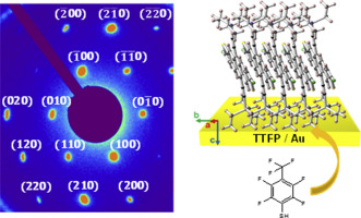
Soluble small molecule organic semiconductors combine the high-performance of small molecule organic semiconductors with the versatile processability of polymeric materials, but the control of device performance and uniformity is challenged by the complex film microstructure formed in these materials, and its strong dependence on processing conditions. These films crystallize via a nucleation and growth mechanism that can be difficult to control. In this study we used highly fluorinated self-assembled monolayers (SAMs) to modify the surface of the source and drain contacts and improve the performance of organic thin-film transistors (OTFTs) through controlling film microstructure and lowering the contact resistance. We reached charge carrier mobilities as high as 5.7 cm2/V in 2,8-Difluoro-5,11-bis(triethylsilylethynyl) anthradithiophene (diF-TES ADT), one order of magnitude greater than what we obtained in devices on untreated substrates, and on par with the value reported for single crystal devices. Kelvin probe measurements distinguished an increase in the work function between 0.28 eV and 0.5 eV, depending on the molecular structure of the SAM. Selected area electron diffraction (SAED) confirmed the preferential “edge-on” molecular orientation of the semiconductor. We discuss the device performance in relation to the film morphology and contact resistance.
中文翻译:
接口工程可增强溶液沉积有机晶体管中的电荷注入和传输
可溶性小分子有机半导体将小分子有机半导体的高性能与聚合物材料的通用加工性能相结合,但是器件性能和均匀性的控制受到这些材料中形成的复杂膜微结构及其对加工条件的强烈依赖的挑战。 。这些膜通过可能难以控制的成核和生长机理结晶。在这项研究中,我们使用高度氟化的自组装单分子层(SAM)来修饰源极和漏极触点的表面,并通过控制薄膜微结构和降低接触电阻来改善有机薄膜晶体管(OTFT)的性能。我们达到了5.7 cm 2的载流子迁移率/ V在2,8-二氟-5,11-双(三乙基甲硅烷基乙炔基)蒽噻吩(diF-TES ADT)中,比我们在未经处理的基板上的设备中获得的值大一个数量级,并且与报告的单晶值相当设备。根据SAM的分子结构,开尔文(Kelvin)探针的测量值可以将功函数的增加区分在0.28 eV和0.5 eV之间。选定区域的电子衍射(SAED)确认了半导体的优先“边上”分子取向。我们讨论了与膜形态和接触电阻有关的器件性能。


 京公网安备 11010802027423号