Organic Electronics ( IF 2.7 ) Pub Date : 2017-08-03 , DOI: 10.1016/j.orgel.2017.08.004 Andrey N. Aleshin , Igor P. Shcherbakov , Ekaterina V. Gushchina , Leo B. Matyushkin , Vyacheslav A. Moshnikov
|
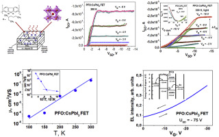
We have designed and investigated electrical and optical properties of solution-processed organic field-effect transistors (OFETs) based on conjugated polymer PFO and perovskite –cesium lead halide nanocrystals (CsPbI3) composite films. It was shown that OFETs based on PFO:CsPbI3 films exhibit current-voltage (I-V) characteristics of OFETs with dominant hole transport and saturation current behavior at temperatures 200–300 K. It was found that PFO:CsPbI3 OFETs have a negligible hysteresis of output and transfer characteristics especially at temperatures below 250 K. The values of the hole mobility estimated from I-Vs of PFO:CsPbI3 OFETs were found to be ∼2.4 10−1 cm2/Vs and ∼1.9 10−1 cm2/Vs in saturation and low fields regimes respectively at 300 K; the hole mobility dropped down to ∼6 10−3 cm2/Vs and 2.8 10−3 cm2/Vs respectively at 200 K, and then down to 5.5 10−5 cm2/Vs at 100 K (in low field regime), which is characteristic of hopping conduction. The effect of sensitivity to light and light-emitting effect were found under application of negative source-drain and gate pulse voltages to PFO:CsPbI3 OFETs at 300 K. The mechanism of charge carrier transport in OFETs based on PFO:CsPbI3 hybrid films is discussed.
中文翻译:
基于聚芴-卤化铯铅纳米晶体复合膜的固溶处理场效应晶体管,其输出和传输特性的磁滞小
我们已经设计和研究了基于共轭聚合物PFO和钙钛矿-铯铯卤化铅纳米晶体(CsPbI 3)复合膜的溶液处理有机场效应晶体管(OFET)的电学和光学特性。结果表明,基于PFO:CsPbI 3薄膜的OFET具有在200-300 K的温度下具有主要空穴传输和饱和电流行为的OFET的电流-电压(IV)特性。发现PFO:CsPbI 3 OFET的磁滞可忽略不计输出和传输特性的变化,尤其是在低于250 K的温度下。根据PFO:CsPbI 3 OFET的I-Vs估算的空穴迁移率值约为2.4 10 -1 cm 2 / Vs和1.9 10在300 K饱和和低场条件下分别为-1 cm 2 / Vs;空穴迁移率在200 K下分别下降至〜6 10 -3 cm 2 / Vs和2.8 10 -3 cm 2 / Vs,然后在100 K下下降至5.5 10 -5 cm 2 / Vs(在低场条件下) ,这是跳跃传导的特征。在300 K的PFO:CsPbI 3 OFET上施加负源极-漏极和栅极脉冲电压时,发现了对光的敏感性和发光效果的影响。基于PFO:CsPbI 3杂化膜的OFET中的电荷载流子传输机理讨论。


 京公网安备 11010802027423号