当前位置:
X-MOL 学术
›
Adv. Mater.
›
论文详情
Our official English website, www.x-mol.net, welcomes your
feedback! (Note: you will need to create a separate account there.)
Tailoring Semiconductor Lateral Multijunctions for Giant Photoconductivity Enhancement
Advanced Materials ( IF 27.4 ) Pub Date : 2017-09-11 , DOI: 10.1002/adma.201703680 Yutsung Tsai,Zhaodong Chu,Yimo Han,Chih-Piao Chuu,Di Wu,Alex Johnson,Fei Cheng,Mei-Yin Chou,David A. Muller,Xiaoqin Li,Keji Lai,Chih-Kang Shih
Advanced Materials ( IF 27.4 ) Pub Date : 2017-09-11 , DOI: 10.1002/adma.201703680 Yutsung Tsai,Zhaodong Chu,Yimo Han,Chih-Piao Chuu,Di Wu,Alex Johnson,Fei Cheng,Mei-Yin Chou,David A. Muller,Xiaoqin Li,Keji Lai,Chih-Kang Shih
|
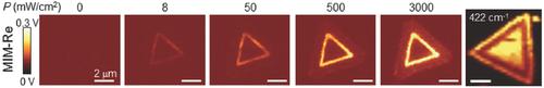
Semiconductor heterostructures have played a critical role as the enabler for new science and technology. The emergence of transition‐metal dichalcogenides (TMDs) as atomically thin semiconductors has opened new frontiers in semiconductor heterostructures either by stacking different TMDs to form vertical heterojunctions or by stitching them laterally to form lateral heterojunctions via direct growth. In conventional semiconductor heterostructures, the design of multijunctions is critical to achieve carrier confinement. Analogously, successful synthesis of a monolayer WS2/WS2(1−x)Se2x/WS2 multijunction lateral heterostructure via direct growth by chemical vapor deposition is reported. The grown structures are characterized by Raman, photoluminescence, and annular dark‐field scanning transmission electron microscopy to determine their lateral compositional profile. More importantly, using microwave impedance microscopy, it is demonstrated that the local photoconductivity in the alloy region can be tailored and enhanced by two orders of magnitude over pure WS2. Finite element analysis confirms that this effect is due to the carrier diffusion and confinement into the alloy region. This work exemplifies the technological potential of atomically thin lateral heterostructures in optoelectronic applications.
中文翻译:

量身定制半导体横向多结,以增强光电导性
半导体异质结构作为新科学和技术的推动者发挥了关键作用。过渡金属二硫化氢(TMD)作为原子薄半导体的出现,通过堆叠不同的TMD形成垂直异质结,或者通过横向缝制它们以通过直接生长形成横向异质结,在半导体异质结构中开辟了新的领域。在常规的半导体异质结构中,多结的设计对于实现载流子限制至关重要。类似地,成功合成了单层WS 2 / WS 2(1- x) Se 2 x / WS 2报道了通过化学气相沉积直接生长产生的多结横向异质结构。生长的结构的特征是拉曼光谱,光致发光和环形暗场扫描透射电子显微镜确定其横向组成轮廓。更重要的是,使用微波阻抗显微镜,证明了可以调整合金区域中的局部光电导率,并使其比纯WS 2高两个数量级。有限元分析证实,这种影响是由于载流子扩散和限制进入合金区域所致。这项工作例证了在光电应用中原子薄的横向异质结构的技术潜力。
更新日期:2017-09-11
中文翻译:
量身定制半导体横向多结,以增强光电导性
半导体异质结构作为新科学和技术的推动者发挥了关键作用。过渡金属二硫化氢(TMD)作为原子薄半导体的出现,通过堆叠不同的TMD形成垂直异质结,或者通过横向缝制它们以通过直接生长形成横向异质结,在半导体异质结构中开辟了新的领域。在常规的半导体异质结构中,多结的设计对于实现载流子限制至关重要。类似地,成功合成了单层WS 2 / WS 2(1- x) Se 2 x / WS 2报道了通过化学气相沉积直接生长产生的多结横向异质结构。生长的结构的特征是拉曼光谱,光致发光和环形暗场扫描透射电子显微镜确定其横向组成轮廓。更重要的是,使用微波阻抗显微镜,证明了可以调整合金区域中的局部光电导率,并使其比纯WS 2高两个数量级。有限元分析证实,这种影响是由于载流子扩散和限制进入合金区域所致。这项工作例证了在光电应用中原子薄的横向异质结构的技术潜力。


 京公网安备 11010802027423号