Nano Research ( IF 9.5 ) Pub Date : 2018-08-02 , DOI: 10.1007/s12274-017-1793-y Qi Jia , Xin Ou , Manuel Langer , Benjamin Schreiber , Jörg Grenzer , Pablo F. Siles , Raul D. Rodriguez , Kai Huang , Ye Yuan , Alireza Heidarian , René Hübner , Tiangui You , Wenjie Yu , Kilian Lenz , Jürgen Lindner , Xi Wang , Stefan Facsko
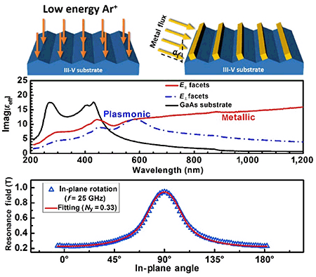
A nanofabrication method for the production of ultra-dense planar metallic nanowire arrays scalable to wafer-size is presented. The method is based on an efficient template deposition process to grow diverse metallic nanowire arrays with extreme regularity in only two steps. First, III–V semiconductor substrates are irradiated by a low-energy ion beam at an elevated temperature, forming a highly ordered nanogroove pattern by a “reverse epitaxy” process due to self-assembly of surface vacancies. Second, diverse metallic nanowire arrays (Au, Fe, Ni, Co, FeAl alloy) are fabricated on these III–V templates by deposition at a glancing incidence angle. This method allows for the fabrication of metallic nanowire arrays with periodicities down to 45 nm scaled up to wafer-size fabrication. As typical noble and magnetic metals, the Au and Fe nanowire arrays produced here exhibited large anisotropic optical and magnetic properties, respectively. The excitation of localized surface plasmon resonances (LSPRs) of the Au nanowire arrays resulted in a high electric field enhancement, which was used to detect phthalocyanine (CoPc) in surface-enhanced Raman scattering (SERS). Furthermore, the Fe nanowire arrays showed a very high in-plane magnetic anisotropy of approximately 412 mT, which may be the largest in-plane magnetic anisotropy field yet reported that is solely induced via shape anisotropy within the plane of a thin film.
中文翻译:
具有非常大的各向异性光学和磁性特性的超密集平面金属纳米线阵列
提出了一种纳米制造方法,用于生产可扩展至晶圆尺寸的超高密度平面金属纳米线阵列。该方法基于有效的模板沉积过程,仅需两个步骤即可以极高的规则性生长各种金属纳米线阵列。首先,III-V半导体衬底在升高的温度下受到低能离子束的照射,由于表面空位的自组装,通过“反向外延”工艺形成了高度有序的纳米沟槽图案。其次,在这些III–V模板上通过以掠入的入射角进行沉积,制造了各种金属纳米线阵列(Au,Fe,Ni,Co,FeAl合金)。该方法允许以周期低至45nm的金属纳米线阵列的规模扩大到晶片尺寸的制造。作为典型的贵金属和磁性金属,这里生产的金和铁纳米线阵列分别显示出大的各向异性光学和磁性。Au纳米线阵列的局部表面等离子体激元共振(LSPRs)的激发导致了高电场增强,该电场增强被用于检测表面增强拉曼散射(SERS)中的酞菁(CoPc)。此外,Fe纳米线阵列显示出约412 mT的非常高的面内磁各向异性,这可能是迄今报道的最大的面内磁各向异性场,仅通过薄膜平面内的形状各向异性引起。用于检测表面增强拉曼散射(SERS)中的酞菁(CoPc)。此外,Fe纳米线阵列显示出约412 mT的非常高的面内磁各向异性,这可能是迄今报道的最大的面内磁各向异性场,仅通过薄膜平面内的形状各向异性引起。用于检测表面增强拉曼散射(SERS)中的酞菁(CoPc)。此外,Fe纳米线阵列显示出约412 mT的非常高的面内磁各向异性,这可能是迄今报道的最大的面内磁各向异性场,仅通过薄膜平面内的形状各向异性引起。


 京公网安备 11010802027423号