当前位置:
X-MOL 学术
›
Mater. Chem. Front.
›
论文详情
Our official English website, www.x-mol.net, welcomes your
feedback! (Note: you will need to create a separate account there.)
A photoacid generator integrated terpolymer for electron beam lithography applications: sensitive resist with pattern transfer potential†
Materials Chemistry Frontiers ( IF 6.0 ) Pub Date : 2017-05-17 00:00:00 , DOI: 10.1039/c7qm00140a Santu Nandi 1, 2, 3, 4 , Midathala Yogesh 1, 2, 3, 4 , Pulikanti Guruprasad Reddy 1, 2, 3, 4 , Satinder K. Sharma 2, 3, 4, 5 , Chullikkattil P. Pradeep 1, 2, 3, 4 , Subrata Ghosh 1, 2, 3, 4 , Kenneth E. Gonsalves 1, 2, 3, 4
Materials Chemistry Frontiers ( IF 6.0 ) Pub Date : 2017-05-17 00:00:00 , DOI: 10.1039/c7qm00140a Santu Nandi 1, 2, 3, 4 , Midathala Yogesh 1, 2, 3, 4 , Pulikanti Guruprasad Reddy 1, 2, 3, 4 , Satinder K. Sharma 2, 3, 4, 5 , Chullikkattil P. Pradeep 1, 2, 3, 4 , Subrata Ghosh 1, 2, 3, 4 , Kenneth E. Gonsalves 1, 2, 3, 4
Affiliation
|
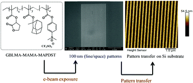
While developing a new resist for different lithography applications, starting from high to low nodes, the potential of the resist in successful pattern transfer has been the key for practical applications particularly in semiconductor industries. Although semiconductor industries are looking for materials for sub 7 nm node technology for sophisticated electronic appliances, the materials with potential for high resolution larger node pattern transfer are equally important for specialized applications in CMOS technology. In this regard, a new ionic photoacid generator included terpolymer photoresist viz GBLMA–MAMA–MAPDST has been synthesized for next generation lithography (NGL) applications. Electron beam lithography (EBL) studies of this resist coated thin films have shown that the resist can pattern 100 nm line/space features under e-beam exposure. The sensitivity (E0) and contrast (γ) were calculated to be 36.5 μC cm−2 and 0.08 respectively. Finally, transfer of 100 nm (line/space) patterns into a silicon substrate has been achieved using a dry plasma etching technique.
中文翻译:

用于电子束光刻应用的光生酸剂集成三元共聚物:具有图案转移电势的敏感抗蚀剂†
在为从高到低节点的不同光刻应用开发新的抗蚀剂时,抗蚀剂在成功的图案转移中的潜力一直是实际应用的关键,特别是在半导体工业中。尽管半导体行业正在寻找用于精密电子设备的7纳米以下节点技术的材料,但具有高分辨率,更大的节点图案转移潜力的材料对于CMOS技术中的特殊应用同样重要。在这方面,一种新的离子型光致产酸剂包括三元共聚物光致抗蚀剂,即GBLMA–MAMA–MAPDST已被合成用于下一代光刻(NGL)应用。对这种抗蚀剂涂覆的薄膜的电子束光刻(EBL)研究表明,该抗蚀剂可以在电子束曝光下对100 nm的线/空间特征进行图案化。计算出的灵敏度(E 0)和对比度(γ)分别为36.5μCcm -2和0.08。最终,使用干法等离子体蚀刻技术已经实现了将100 nm(线/空)图案转移到硅基板中。
更新日期:2017-05-17
中文翻译:
用于电子束光刻应用的光生酸剂集成三元共聚物:具有图案转移电势的敏感抗蚀剂†
在为从高到低节点的不同光刻应用开发新的抗蚀剂时,抗蚀剂在成功的图案转移中的潜力一直是实际应用的关键,特别是在半导体工业中。尽管半导体行业正在寻找用于精密电子设备的7纳米以下节点技术的材料,但具有高分辨率,更大的节点图案转移潜力的材料对于CMOS技术中的特殊应用同样重要。在这方面,一种新的离子型光致产酸剂包括三元共聚物光致抗蚀剂,即GBLMA–MAMA–MAPDST已被合成用于下一代光刻(NGL)应用。对这种抗蚀剂涂覆的薄膜的电子束光刻(EBL)研究表明,该抗蚀剂可以在电子束曝光下对100 nm的线/空间特征进行图案化。计算出的灵敏度(E 0)和对比度(γ)分别为36.5μCcm -2和0.08。最终,使用干法等离子体蚀刻技术已经实现了将100 nm(线/空)图案转移到硅基板中。


 京公网安备 11010802027423号