当前位置:
X-MOL 学术
›
Chem. Rev.
›
论文详情
Our official English website, www.x-mol.net, welcomes your
feedback! (Note: you will need to create a separate account there.)
Chemical Modification of Semiconductor Surfaces for Molecular Electronics
Chemical Reviews ( IF 51.4 ) Pub Date : 2017-02-23 00:00:00 , DOI: 10.1021/acs.chemrev.6b00746 Ayelet Vilan 1 , David Cahen 1
Chemical Reviews ( IF 51.4 ) Pub Date : 2017-02-23 00:00:00 , DOI: 10.1021/acs.chemrev.6b00746 Ayelet Vilan 1 , David Cahen 1
Affiliation
|
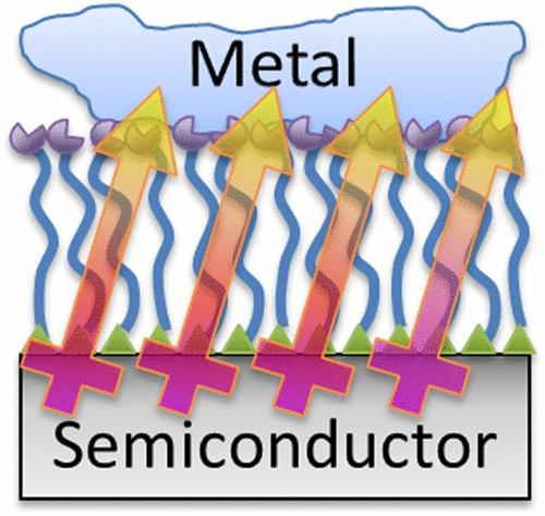
Inserting molecular monolayers within metal/semiconductor interfaces provides one of the most powerful expressions of how minute chemical modifications can affect electronic devices. This topic also has direct importance for technology as it can help improve the efficiency of a variety of electronic devices such as solar cells, LEDs, sensors, and possible future bioelectronic ones. The review covers the main aspects of using chemistry to control the various aspects of interface electrostatics, such as passivation of interface states and alignment of energy levels by intrinsic molecular polarization, as well as charge rearrangement with the adjacent metal and semiconducting contacts. One of the greatest merits of molecular monolayers is their capability to form excellent thin dielectrics, yielding rich and unique current–voltage characteristics for transport across metal/molecular monolayer/semiconductor interfaces. We explain the interplay between the monolayer as tunneling barrier on the one hand, and the electrostatic barrier within the semiconductor, due to its space-charge region, on the other hand, as well as how different monolayer chemistries control each of these barriers. Practical tools to experimentally identify these two barriers and distinguish between them are given, followed by a short look to the future. This review is accompanied by another one, concerning the formation of large-area molecular junctions and charge transport that is dominated solely by molecules.
中文翻译:

用于分子电子学的半导体表面的化学改性
在金属/半导体界面中插入分子单分子层提供了最有力的表达之一,即微小的化学修饰如何影响电子设备。该主题对技术也具有直接重要性,因为它可以帮助提高各种电子设备的效率,例如太阳能电池,LED,传感器和可能的未来生物电子设备。综述涵盖了使用化学方法控制界面静电的各个方面的主要方面,例如界面态的钝化和通过固有分子极化进行的能级对齐,以及与相邻金属和半导体触点的电荷重排。分子单分子层的最大优点之一是它们能够形成出色的薄电介质,金属/分子单层/半导体界面。我们一方面解释了单层作为隧穿势垒,另一方面由于其空间电荷区而使半导体内部的静电势垒之间的相互作用,以及不同的单层化学如何控制这些势垒中的每一个。给出了通过实验确定这两个障碍并加以区分的实用工具,然后简要展望了未来。这篇评论还伴随着另一篇有关大面积分子结的形成和仅由分子控制的电荷传输的评论。
更新日期:2017-02-23
中文翻译:
用于分子电子学的半导体表面的化学改性
在金属/半导体界面中插入分子单分子层提供了最有力的表达之一,即微小的化学修饰如何影响电子设备。该主题对技术也具有直接重要性,因为它可以帮助提高各种电子设备的效率,例如太阳能电池,LED,传感器和可能的未来生物电子设备。综述涵盖了使用化学方法控制界面静电的各个方面的主要方面,例如界面态的钝化和通过固有分子极化进行的能级对齐,以及与相邻金属和半导体触点的电荷重排。分子单分子层的最大优点之一是它们能够形成出色的薄电介质,金属/分子单层/半导体界面。我们一方面解释了单层作为隧穿势垒,另一方面由于其空间电荷区而使半导体内部的静电势垒之间的相互作用,以及不同的单层化学如何控制这些势垒中的每一个。给出了通过实验确定这两个障碍并加以区分的实用工具,然后简要展望了未来。这篇评论还伴随着另一篇有关大面积分子结的形成和仅由分子控制的电荷传输的评论。


 京公网安备 11010802027423号