
Linear Active Disturbance Rejection Control of New Double Full-Bridge ZVZCS Converter for Beam Supply
1
School of New Energy and Power Engineering, Lanzhou Jiaotong University, Lanzhou 730070, China
2
School of Automation and Electrical Engineering, Lanzhou Jiaotong University, Lanzhou 730070, China
3
Lanzhou Institute of Physics, Lanzhou 730000, China
*
Author to whom correspondence should be addressed.
Electronics 2022, 11(19), 3062; https://doi.org/10.3390/electronics11193062
Submission received: 19 August 2022
/
Revised: 12 September 2022
/
Accepted: 23 September 2022
/
Published: 26 September 2022
(This article belongs to the Special Issue Advanced Technologies in Power Electronics and Motor Drives)
Abstract
:In view of the unstable output voltage of the new double full bridge ZVZCS converter of beam power supply when it is disturbed by external disturbance or internal parameter change in practical application, combined with the characteristics of the beam power supply system model, this paper proposes a beam power supply control strategy based on linear active disturbance rejection control (LADRC). Firstly, the working principle of the new double full bridge ZVZCS converter of beam power supply is analyzed, and considering the parasitic parameters and effective duty cycle of circuit components, the small signal equivalent model under two working modes is established. Secondly, combined with the system model and linear active disturbance rejection control theory, a double closed-loop controller is designed, which takes the second-order LADRC as the outer voltage loop and PI control as the inner current loop. Finally, the simulation and experimental results show that the designed controller has stronger robustness, anti-interference and better dynamic response speed than the traditional double closed-loop PI controller in load switching and dual-mode switching, and has a good development prospect.
1. Introduction
Due to its advantage of high specific impulse, electric propulsion technology has been widely used in the field of aerospace at home and abroad [1,2]. Among them, the Power Processing Unit (PPU) is mainly used to provide various voltages and currents required for ion thrusters, including heating, ignition, and ion acceleration, etc., which is the core of ion electric propulsion technology [3,4]. A typical ion thruster PPU consists of a beam supply, an accelerating power supply, an anode power supply, a cathode heating power supply, a cathode ignition power supply, a neutralizer cathode heating power supply, a neutralizer contact power supply, and a neutralizer cathode ignition power supply. The main function of the beam supply is to provide voltage and power to establish the electric field between the two gates of the thruster and the acceleration of Xenon ions. The output voltage can reach 2 kV, and the output power can reach 10 kW, accounting for more than 80% of the output power of the entire PPU, and it is the key point of the PPU design with high efficiency and high reliability [5,6,7,8].
At present, according to the different application environments at home and abroad, the research on the beam supply is mainly shown in the topology structure and control methods. Astrium’s ion thruster beam supply adopts a resonant DC/DC topology for the main circuit, and a push-pull topology for the second conversion circuit to achieve small-range voltage regulation. The topology design is a single control loop, which cannot control the current of the system [9,10,11]. A non-resonant full-bridge circuit is adopted for the beam supply of the thruster of “Deep Space No. 1”, which can meet the wide dynamic range and high power demand. Due to the hard switch, the PPU efficiency will be greatly reduced due to heat consumption [12,13]. The domestically designed LIP-300 ion thruster beam supply is composed of three 500 V/1500 W power supply modules in series. The phase-shifting full-bridge topology is adopted to realize zero voltage and zero current switching (ZVZCS) technology, which reduces the switching loss of the switch tube and improves the product efficiency, keeping the same with foreign countries [14,15].
When the spacecraft is performing space flight missions, different mission stages (such as position maintenance, orbit transfer, attitude control, etc.) require different thrust forces, which require the ion thruster to work in multiple modes. That is, different stages require different thrust forces [15]. Moreover, a wide range of light intensity and temperature will cause a wide range of variations in output power and voltage of the solar array, so an electric propulsion system is required to realize a wide range of multi-point operations [16,17,18].
Therefore, different from other switching power supplies, beam supply has the following main characteristics. The first is to require itself to have the characteristics of short-time high-power output. Second, its load characteristics vary greatly. The third is the multi-mode operation. To improve the performance of the control system and ensure the spacecraft running continuously and stably in orbit, the beam supply usually adopts a mature double closed-loop PI control system of outer voltage loop and inner current loop. However, in space applications, the nonlinear dynamics of the DC converter are quite complex, and it is vulnerable to electromagnetic interference, input line interference, load interference, single-particle flip interference, and so on. In other words, when the system is subject to external disturbance and internal parameters change, the control effect of the double closed-loop PI control system will significantly decrease [19,20].
In the 1980s, researcher Jingqing Han put forward a new nonlinear Control theory, Active Disturbance Rejection Control (ADRC), based on the in-depth study of PID Control. The core idea is that all the uncertain factors acting on the controlled object are reduced to unknown disturbances, and the input and output data are estimated and compensated by the extended observer to improve the disturbance rejection performance and parameter robustness of the system [21,22]. ADRC technology, as a practical design method, has been successfully applied in various engineering fields, especially in high-speed and high-precision control and occasions with obvious external disturbances [23,24,25,26,27]. However, the nonlinear function is introduced into the controller, which increases the complexity of parameter tuning to some extent. To simplify parameter tuning and apply it quickly in practical engineering, Professor Zhiqiang Gao puts forward Linear Active Disturbance Rejection Control (LADRC). The linear function is adopted to control the system, and a new bandwidth parameterization technology is adopted to greatly simplify the parameter setting process [28,29,30]. Many studies have shown that LADRC has not only stronger robustness and disturbance rejection performance but also easy parameter tuning, so it has been successfully applied in many projects [31,32,33,34,35,36,37,38,39].
This paper proposes a new control strategy for beam power supply, that is, a double closed-loop control strategy with LADRC as the outer voltage loop and PI control as the inner current loop, and builds a simulation and experimental platform. Simulation and experiments show that the designed controller has good parameter robustness and anti-interference performance. The structure of this paper is as follows: Section 1 analyzes the working principle of the new double full bridge ZVZCS converter of beam power supply; Section 2 introduces the design of the LADRC controller based on the previous modeling work [40]; in Section 3, the simulation model is built in MATLAB/Simulink; Section 4 gives the experimental results; and Section 5 summarizes the full text.
2. Working Principle of a New Double Full Bridge ZVZCS Converter with Beam Power Supply
2.1. Converter Topology
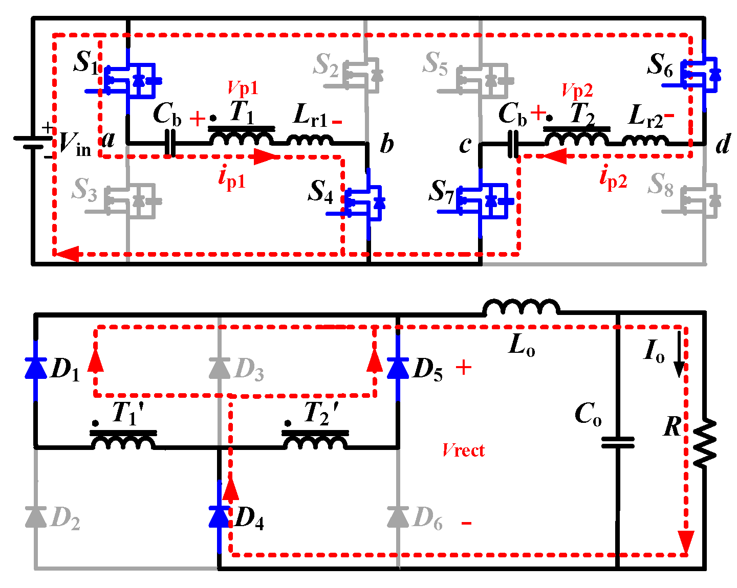
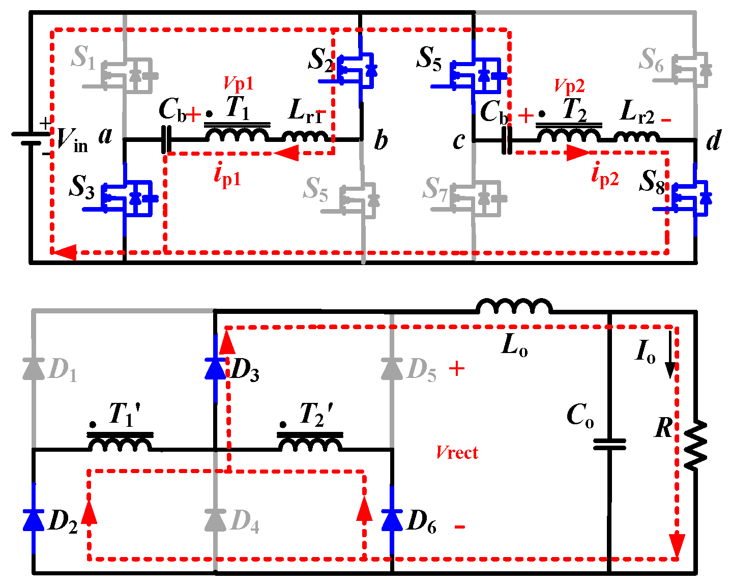
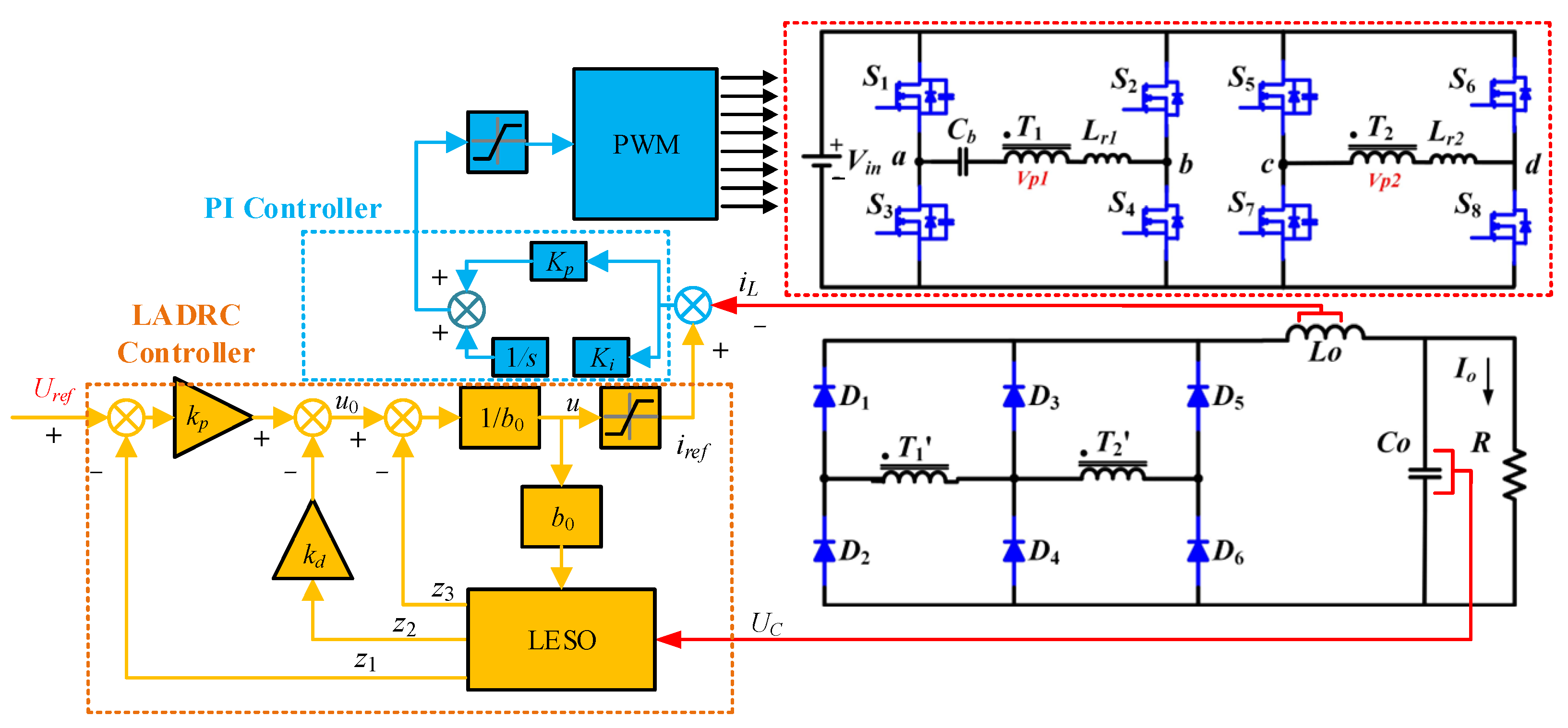
The topology of the new double full-bridge ZVZCS converter of the beam supply is shown in Figure 1. MOSFET S1, S2, S3, S4, blocking capacitor Cb, resonant inductor Lr1, and high-frequency transformer T1 constitute the first bridge; MOSFET S5, S6, S7, S8, resonant inductor Lr2, and high frequency transformer T2 form the second bridge; rectifier diodes D1, D2, D3, D4, D5, and D6 form a hybrid rectifier bridge. The inductance Lo and the capacitance Co are used as the output filtering part.
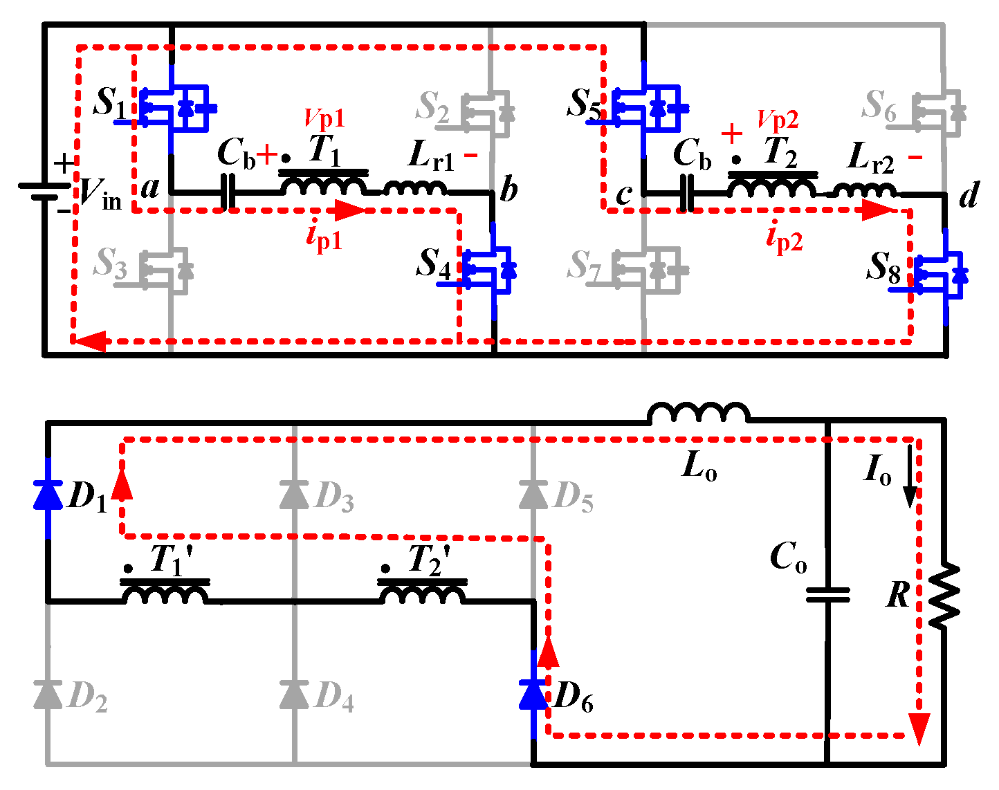
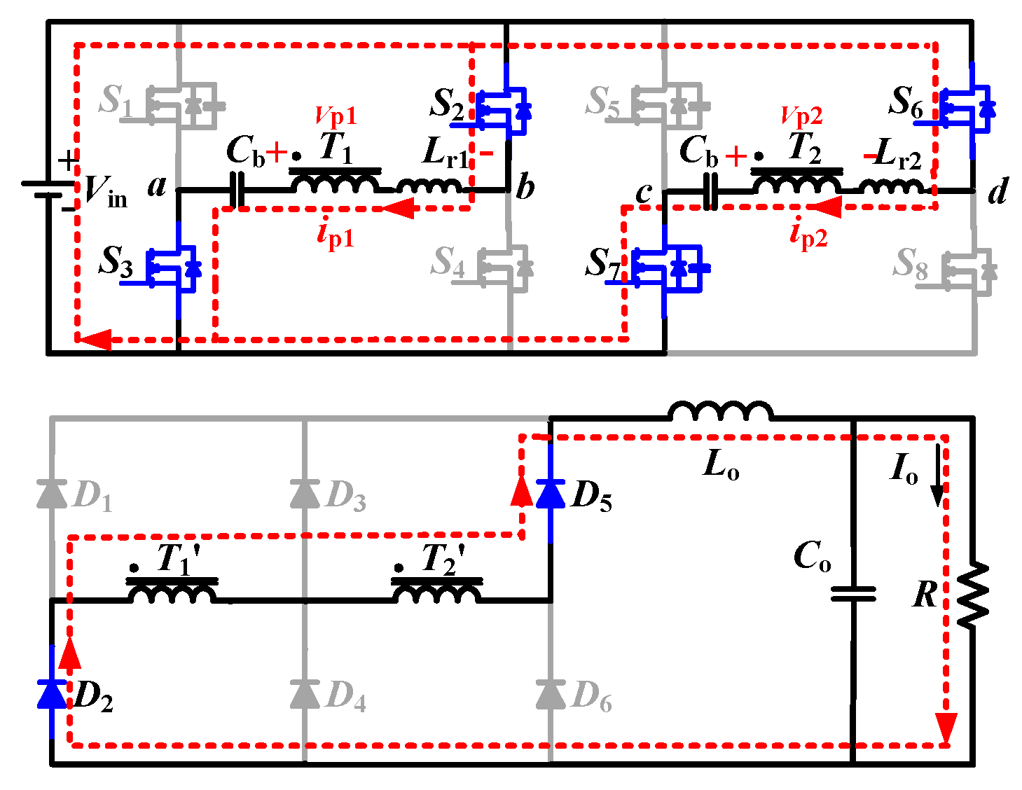
The converter operates in two modes: duty cycle mode and phase shift mode. In duty cycle mode, the two full bridges are input in parallel, and the auxiliary side of the high-frequency transformer is output in parallel. The output voltage is controlled by controlling the duty cycle. The conduction schematic diagram of the first half and the second half period are shown in Figure 2 and Figure 3. In the phase shift mode, the two full bridges are input in parallel, and the auxiliary side of the high-frequency transformer is output in series. The output voltage is controlled by controlling the phase shift angle. The ZVZCS soft switching technology is realized to reduce power consumption and improve the efficiency of the converter. Figure 4 and Figure 5 are the conduction schematics of the first half period and the second half period. The structure of input parallel, output series, and parallel can effectively reduce the current stress of the MOSFET and meet the requirements of the wide range voltage output of the beam supply under the condition of the variable thrust of the thruster to the maximum extent [41,42,43]. The converter can achieve an 80–160 V wide range of DC input, 0–1800 V wide range of DC output, single power 2 kW, suitable for low-voltage large current input, high-voltage output occasions, and can improve the power of the whole machine through multi-module current sharing technology. The hybrid rectifier bridge does not require additional components to prevent the reverse flow of the primary current during the commutation interval, which not only minimizes the duty ratio loss and on-loss but also reduces the cost. In addition, the low voltage stress of the intermediate bridge-arm shared diode is also obtained [44,45,46].
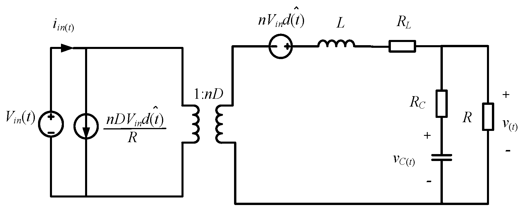
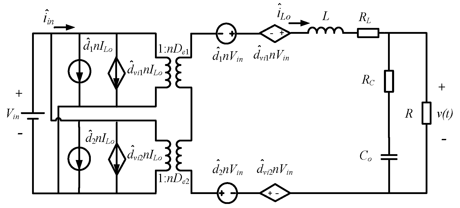
2.2. Small-Signal Model of the Converter
To study the characteristics of the converter and improve its rapidness and stability, the small-signal modeling of the new double-full-bridge soft-switching converter is carried out by using the state-space averaging method and considering the parasitic resistance of the output filter inductor and the output filter capacitor. This task has been completed in the early stage, and the results are directly presented in this paper. The detailed modeling process can be found in the literature [40].
3. Design of LADRC Controller
3.1. Structure of LADRC
At present, the control strategy used for beam supply is mature double closed-loop PI control. However, its control effect is significantly reduced due to the large load characteristic of the beam supply, the requirement of short time high-power output, and the interference of external and internal parameter changes. Therefore, good disturbance rejection performance and parameter robustness are the key characteristics of the beam supply. Active Disturbance Rejection Control (ADRC) technology can estimate and compensate for the unobservable and mismatched disturbances. Thus, it can better deal with the external and internal disturbances of the system and improve the robustness and anti-interference of the system. Therefore, in this paper, the outer voltage loop PI control is replaced by LADRC, and PI control is used as the inner current loop. The structure diagram of the control system is shown in Figure 8.
Aiming at the internal parameter disturbance and external disturbance of the beam power supply system, firstly, a second-order extended state observer (LESO) is designed to estimate the output voltage, the differential signal of the output voltage and the total disturbance of the system. Secondly, the linear state error feedback (LSEF) control rate is designed to calculate the error signal and the control quantity to realize the disturbance compensation of the system. Finally, the output of the LADRC controller is taken as the given current inner loop. After the calculation of the current inner loop PI, the controlled object will be precisely controlled to ensure the stable and effective operation of the beam supply.
3.2. Design of LADRC
The second-order controlled object is shown in Equation (3).
where y and u are output and input, respectively, w is disturbance, a1, a0, and w are unknown, part b is known, and the known part is b0, then Equation (3) is converted to Equation (4):
where, is the total of external and internal disturbances.
Select the state variable as shown in Equation (5).
Then the equation of state expression is shown in Equation (6).
The vector form is shown in Equation (7).
where, , , , . Then the representation of the extended observer is shown in Equation (8).
where y is the output voltage, z1 is the estimation of the output voltage, z2 is the estimation of the differential signal of the output voltage, z3 is the estimation of the total disturbance suffered by the grid power supply, and the parameters l1, l2, l3 are the gain of the observer. According to the bandwidth method [29], the poles of the characteristic equation are placed at the same position, as shown in Equation (9).
Can be obtained:
where, wo is the bandwidth of the observer.
For the convenience of program operation, the discrete linear extended state observer is shown in Equation (11), and T is the sampling period.
The total disturbance of the system is estimated by the linear state observer. The error control law is used to compensate the error feedback in real time, so as to improve the anti-interference ability of the system. The output z1, z2 of the observer and the input Uref of the reference value are used as the input of the error feedback control rate. The designed error feedback control law is shown in Equation (12).
Because LESO can estimate and compensate the total disturbance in real time, the integrator used to eliminate the static error is no longer needed, and the error feedback control law adopts a simplified PD combination. Where u0 is the output of LSEF, u is the output of control quantity, that is, the output of voltage loop, b0 is the compensation coefficient, kp and kd are the gains of the controller, and the values are:
where wc is the bandwidth of the controller.
For the convenience of program operation, the discrete linear extended state observer is shown in Equation (14):
Through the design of linear state observer and linear error feedback control rate, the setting parameters of LADRC are changed into three, which are: observer bandwidth w0, controller bandwidth wc, and compensation factor b0.
4. Simulation Analysis
In order to further verify the performance of LADRC control, a simulation model is built in MATLAB/Simulink, including a double closed-loop controller with LADRC as the outer voltage loop and PI control as the inner current loop and a double closed-loop system with PI for both the outer voltage loop and the inner current loop. The integral of the time weighted absolute error (ITAE) index of the error signal is used to optimize the parameters of the PI controller. The rapidity, robustness, and anti-interference of the two controllers are compared. The parameters used in the simulation are shown in Table 1.
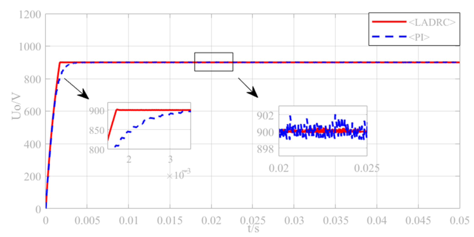
4.1. Step Response
The output voltage is set as 900 V, and the load is 2000 Ω. Response curves of the two controllers are shown in Figure 9 and Figure 10.
The simulation results show that both controllers can achieve stable output without static error, but the adjustment time of LADRC is faster, which is 1.9 ms, and the PI double closed-loop controller needs 3.5 ms. In the steady state, the output ripple of LADRC is smaller, and the standard deviation and range are smaller.
4.2. Anti Interference Analysis
When the input voltage is 100 V and the output voltage is 900 V, the initial output load is 2000 Ω, which suddenly changes to 4000 Ω at 0.01 s and 2000 Ω at 0.03 s. The waveforms of the output voltage and current are shown in Figure 11 and Figure 12.
It can be seen in Figure 11 and Figure 12 that the output voltage rises to a certain extent during 0.01 s load shedding, and the LADRC has a lower overshoot and faster convergence speed than PI control. When the load is increased to 0.03 s, the output voltage decreases to a certain extent, but compared with PI control, linear ADRC has smaller voltage overshoot and faster convergence speed. This shows that the LADRC controller has a stronger ability to suppress voltage drop and faster regulation time after sudden load addition and reduction, which coincides with the advantages of the LADRC controller. It can estimate the load disturbance and compensate it to improve the system’s anti-interference ability.
5. Experimental Verification
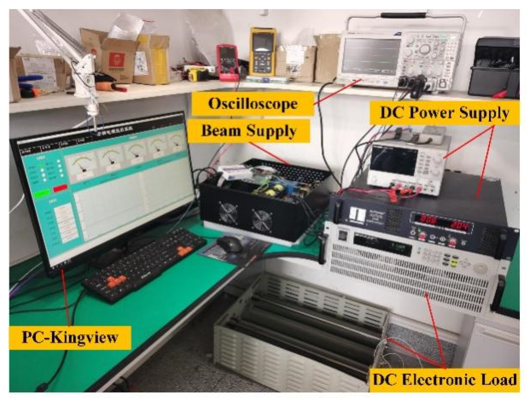
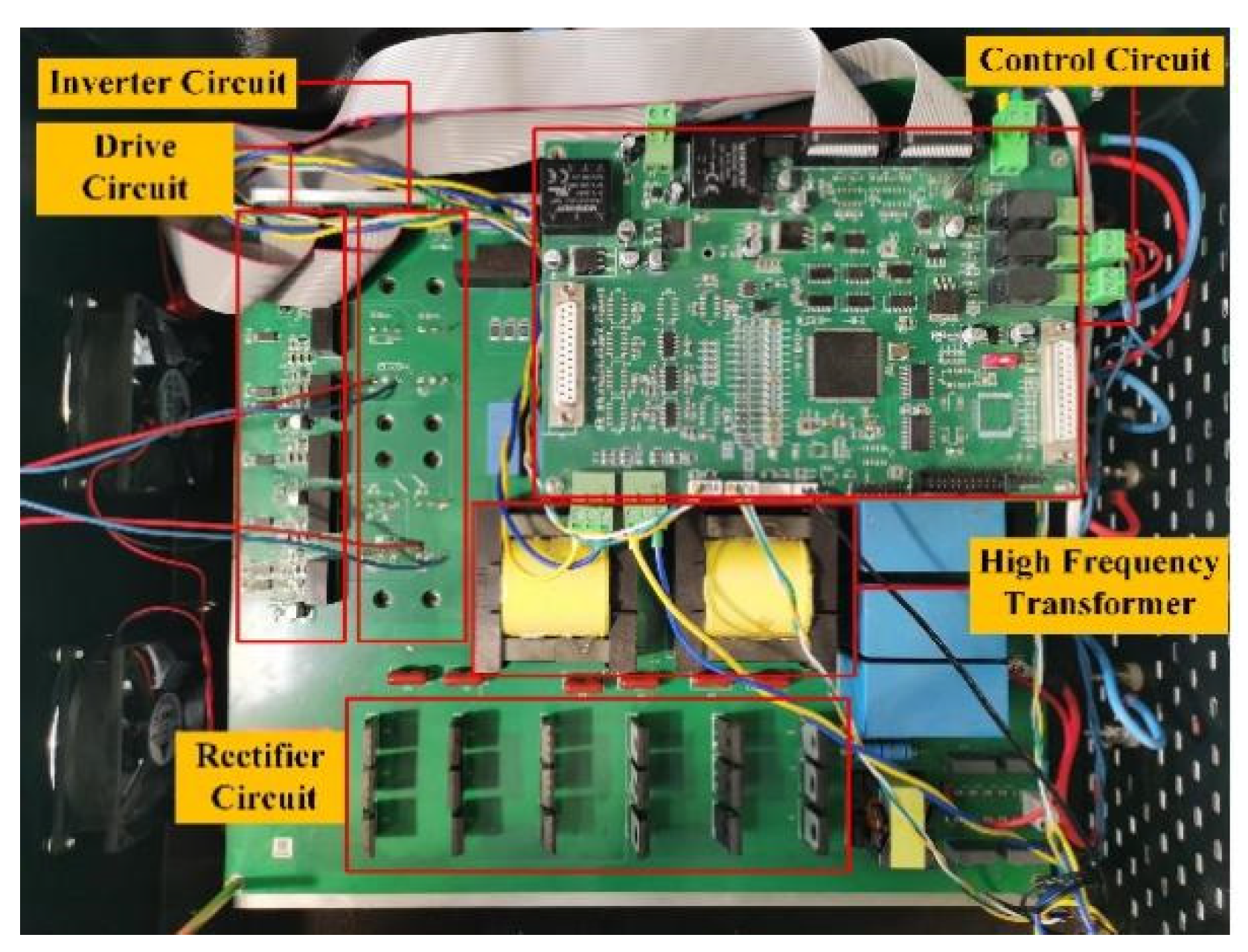
To verify the control effect of the LADRC controller under actual conditions, a 2 kW beam supply prototype is designed based on the TMS320F28335 core processor, as shown in Figure 13 and Figure 14. The experimental instruments used are as follows: DC electronic load, DC power supply, oscilloscope, high-voltage differential probe, current probe, beam supply experimental prototype, Kingview upper computer, etc. The two controllers’ performance was verified by the prototype’s reference mutation, load mutation, and dual mode switching experiments.
5.1. Hardware Design
The technical indicators of the converter and the parameters of the main components used are shown in Table 2 and Table 3. The specific design process is as follows.
- Transformer design;
The transformer transformation ratio is 1:10, and the calculation of primary winding np is shown in Equation (15). Where ∆B is the magnetic flux density and Ae is the effective cross-sectional area of the magnetic flux. The magnetic core selected in this paper is ETD59, and the corresponding parameters are: ∆B = 0.2 T, Ae = 368.4 mm2. The calculation result is that the number of primary turns of transformer is np = 10.9. The actual number of primary turns is taken as 12 T, and the number of secondary turns is 120 T.
- 2.
- Semiconductor device selection;
The voltage and current stress of inverter MOS tube and rectifier diode are shown in Table 4.
According to the parameters in Table 4, the MOS tube with model IXFH50N30Q3 (300 V/50 A) is selected as the switch tube on the inverter side, and the diode with model APT40DQ120BG (1200 V/40 A) is selected as the rectifier tube on the rectifier side.
- 3.
- Design of DC isolating capacitor;
The calculation formula of the isolation capacitance is shown in Equation (16), in which the voltage drop of the isolation capacitance is taken as Vcbp = 10%Vin, so the calculated capacitance value is 4.4 μF. In practical application, two 2.2 μF capacitors are selected in parallel to improve the current carrying capacity.
5.2. Analysis of Experimental Results
- 4.
- Load mutation test;
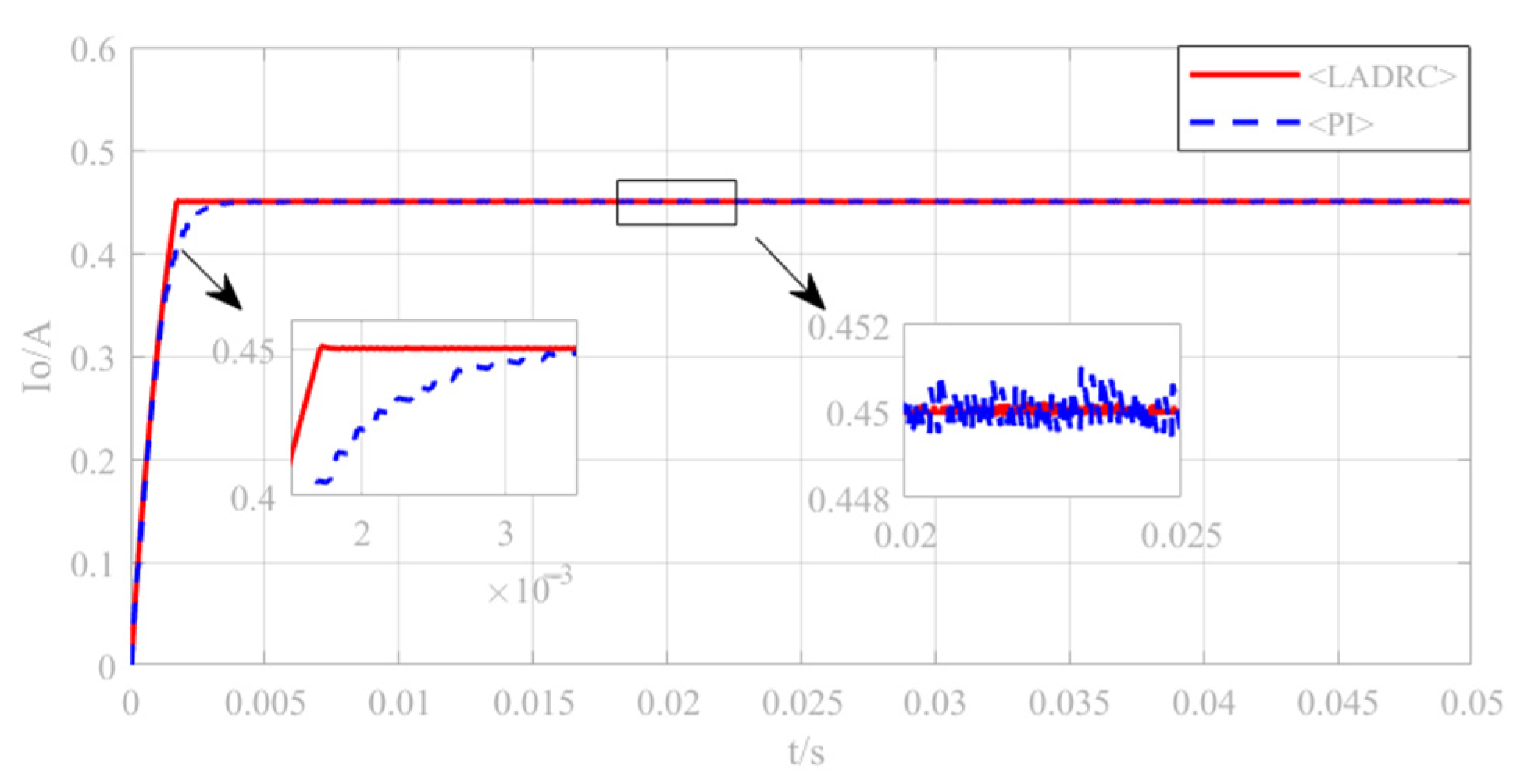
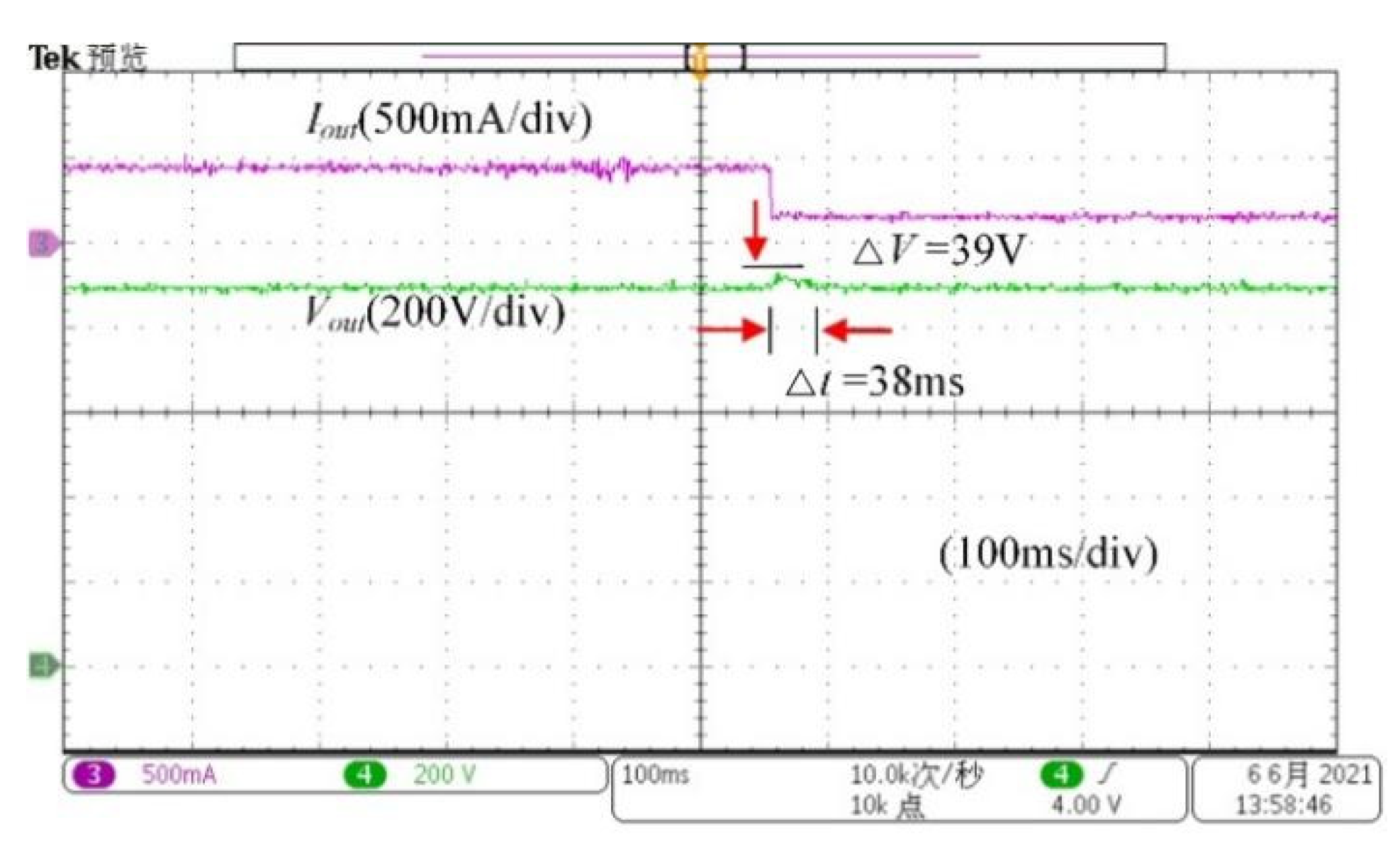
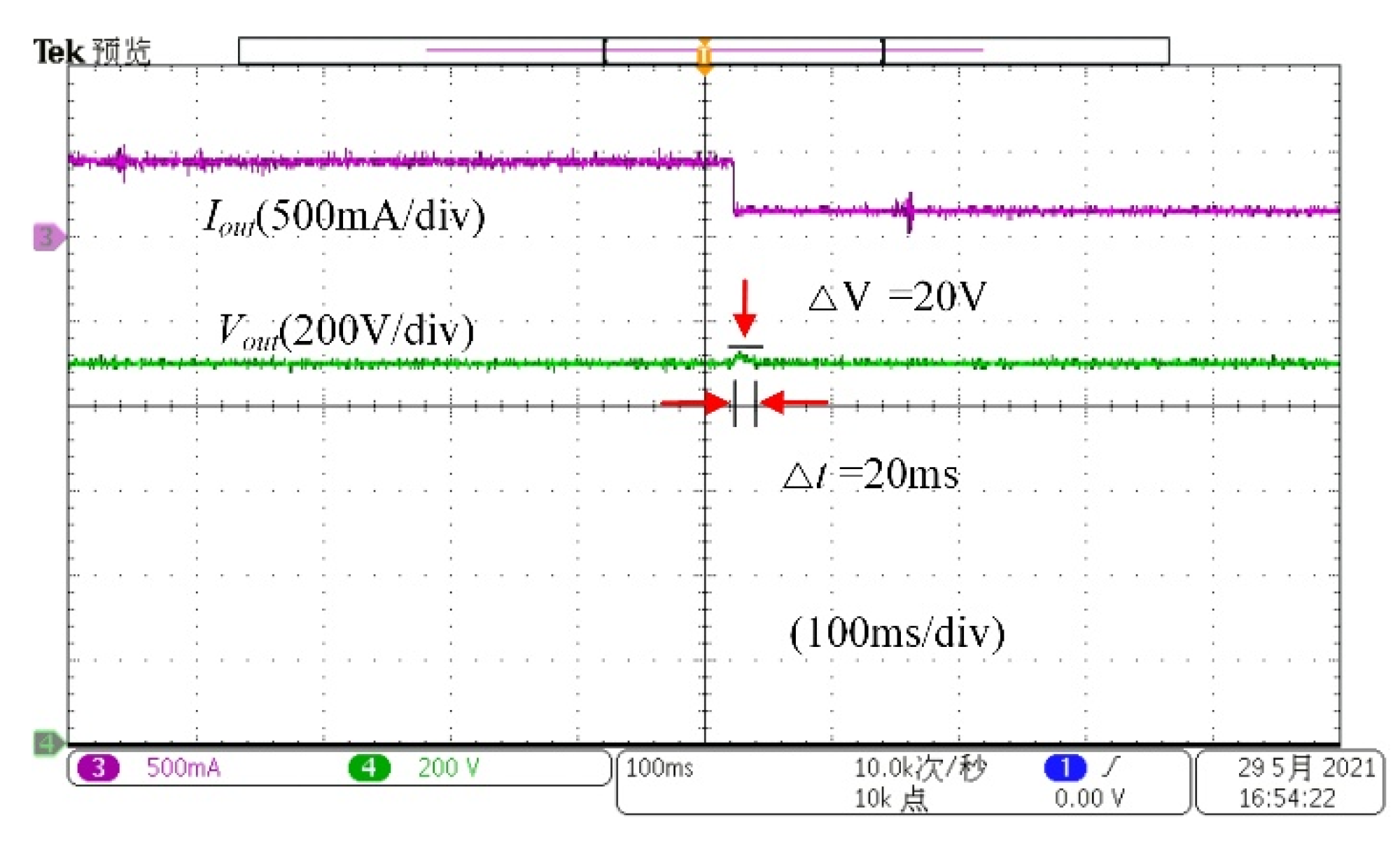
When the output voltage is 900 V and the load changes from 2000 Ω to 6000 Ω, the comparison of voltage and current under the two controllers is shown in Figure 15 and Figure 16, and the statistical table of the experimental results is shown in Table 5.
It can be seen that when the load current changes from 0.45 A to 0.15 A, the output voltage of the double closed-loop PI controller increases by 39 V, and the reference output is tracked within 38 ms. The output voltage of the LADRC controller increases by 20 V and converges within 20 ms.
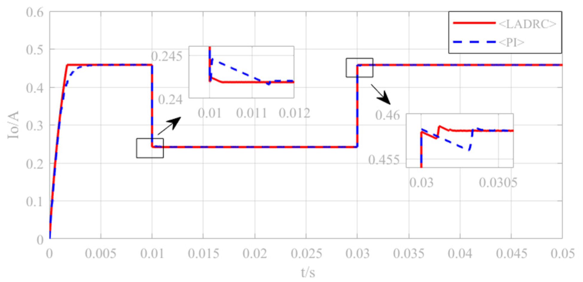
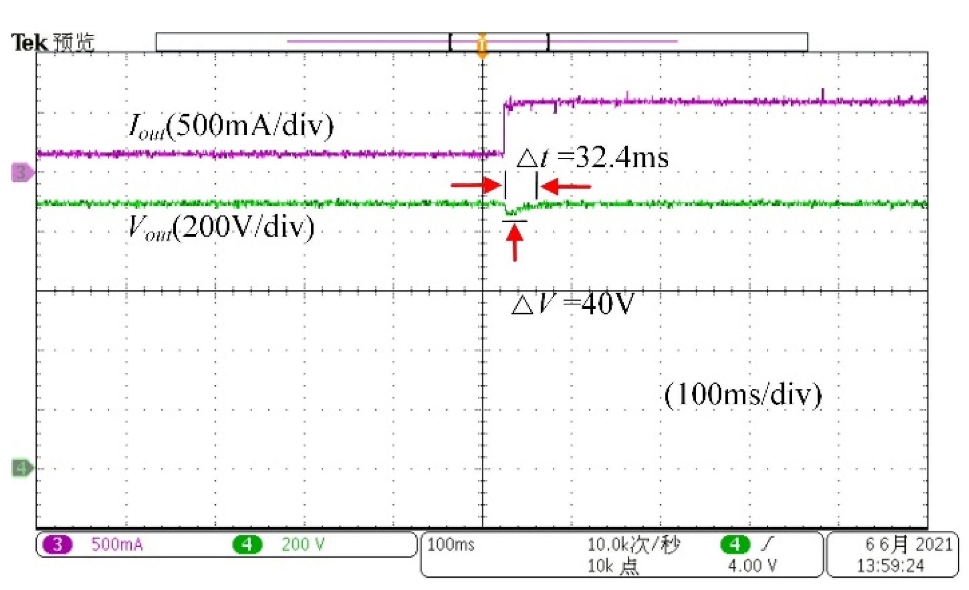
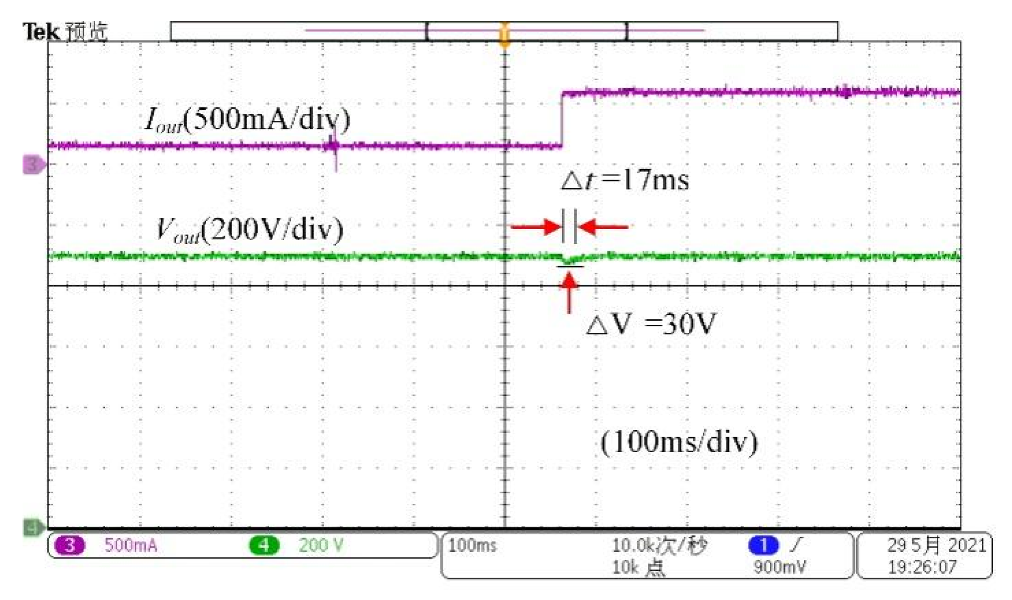
When the output voltage is 900 V, the load resistance changes from 6000 Ω to 1500 Ω. A comparison of voltage and current under the two controllers is shown in Figure 17 and Figure 18. Data statistics of the sudden-increased load experiment results are shown in Table 6.
It can be seen that when the load current changes from 0.15 A to 0.6 A, the output voltage of the double closed-loop PI controller drops 40 V, and the reference output voltage is restored after 32.4 ms, and the adjustment time is relatively slow. The output voltage of the LADRC controller dropped by 30 V and recovered the reference output voltage after 17 ms. After the suddenly increased loading, the LADRC controller has a stronger ability to suppress voltage sags and faster adjustment time, which coincides with the advantages of the LADRC controller. It can estimate the load disturbance and compensate it to improve the anti-interference ability of the system.
- 5.
- Dual mode switching experiment;
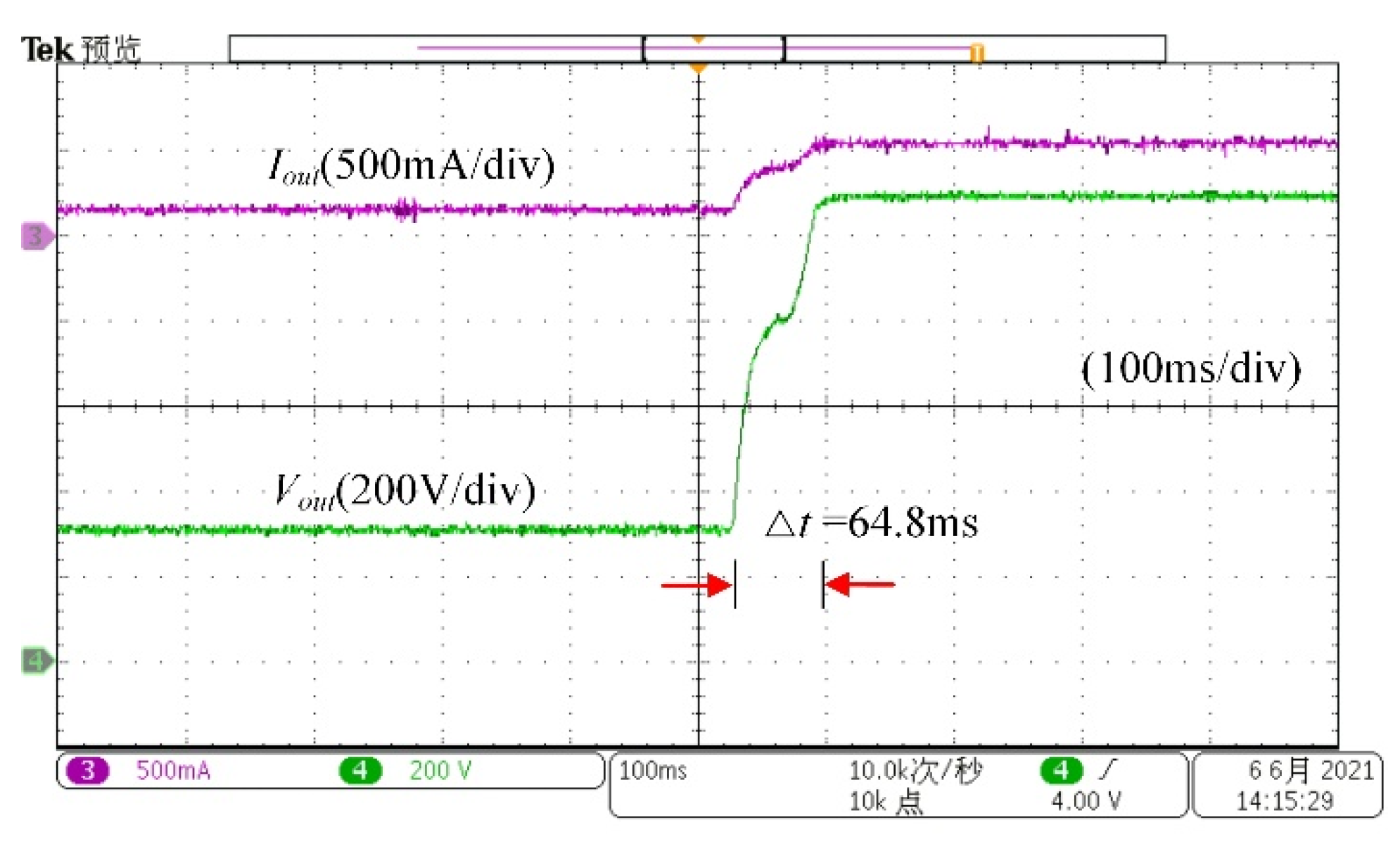
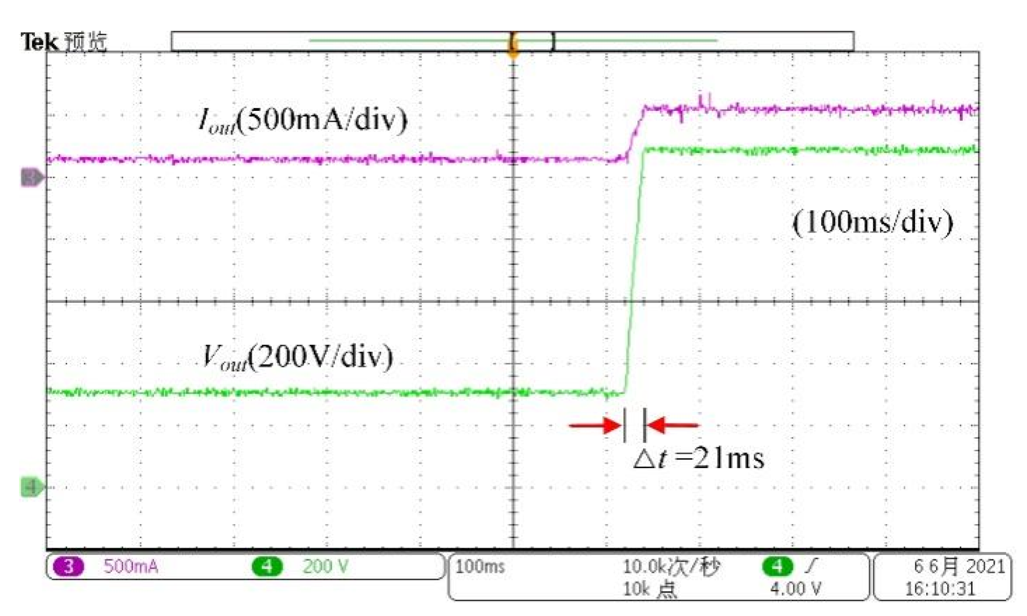
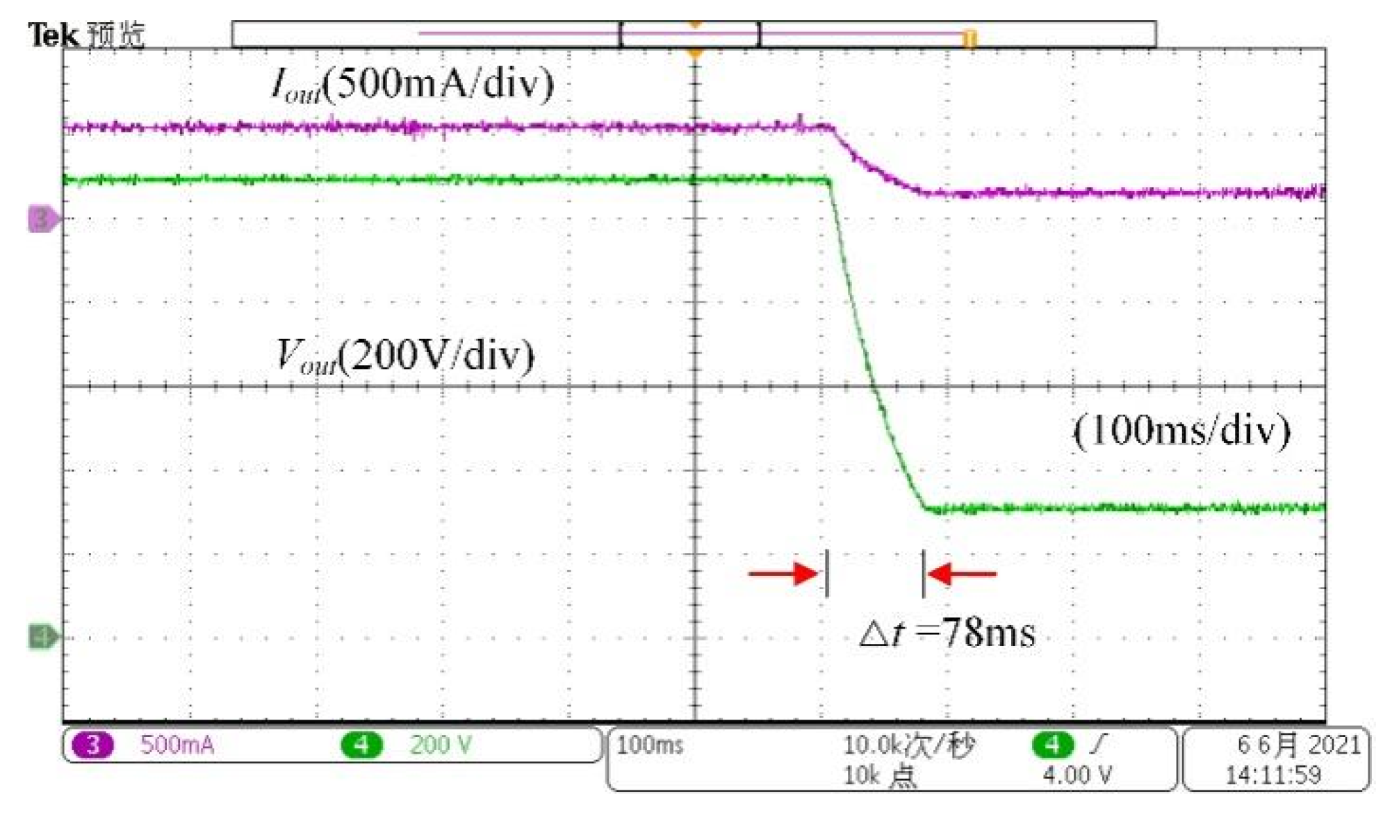
The input voltage is 80 V and the load resistance is 2000 Ω. The output voltage is switched from 300 V to 1100 V, that is, the parallel mode is switched to series mode. Output voltages of the two controllers are shown in Figure 19, Figure 20, Figure 21 and Figure 22. Data statistics of the experimental results of dual-mode switching are shown in Table 7 and Table 8.
Through comparison, it can be found that when the double closed-loop PI controller is switched from parallel mode to series mode, some jitter occurs at the switching point, and the adjustment time is relatively slow. The whole switching time is 64.8 ms and 78 ms. However, when the LADRC controller is switching between two modes, not only does no jitter occur, but also the adjustment time is very fast (21 ms and 74 ms), which realizes the smooth switching between the two modes. It can be seen that the system still has strong adaptability when the internal parameters change. LADRC reduces the uncertain factors acting on the controlled object to the unknown disturbance, and the method of estimating and compensating the input and output data through the extended observer has high robustness.
- 6.
- Soft switching and efficiency test;
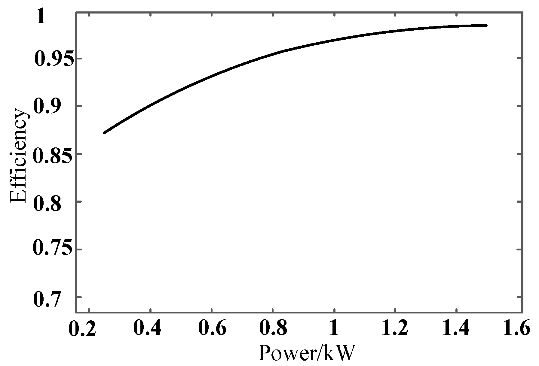
Switching loss is one of the main factors affecting the system efficiency. In order to maximize the system efficiency, ZVS soft switching is implemented in the phase-shifting mode in this paper. The soft switching experimental waveform is shown in Figure 23. The efficiency test was also conducted in this paper. As shown in Figure 24, the efficiency of the system when it works in the duty cycle mode is low, mainly because soft switching is not realized in the duty cycle mode, and the losses of switches and transformers are large. With the increase of the output power of the power supply, the system switches to the phase-shift mode and realizes ZVS, and the efficiency of the power supply increases.
6. Conclusions
For the new double full bridge ZVZCS converter of beam power supply, a new control strategy is proposed in this paper, which is a double closed-loop control structure with linear active disturbance rejection control as the outer voltage loop and PI control as the inner current loop; In order to verify the performance of the designed controller, a simulation model is built in MATLAB/Simulink, and a 2 kW experimental prototype is designed based on DSP28335. The simulation and experimental results show that the proposed control strategy has stronger robustness and anti-interference than the traditional double closed-loop PI control strategy. The system also realizes ZVS soft switching, and the maximum efficiency of the system can reach 97% in phase-shifting mode.
Author Contributions
Conceptualization, H.D. and H.W.; methodology, H.W.; software, H.W. and G.L.; validation, H.W.; formal analysis, H.W. and G.L.; investigation, H.D. and H.W.; resources, H.D. and H.W.; data curation, H.W.; writing—original draft preparation, H.W. and G.L.; writing—review and editing, H.W. and G.L.; visualization, H.Z.; supervision, H.Z.; project administration, H.Z.; funding acquisition, H.Z. All authors have read and agreed to the published version of the manuscript.
Funding
This research was funded by the Major Science and Technology Projects in Gansu Province (18ZD2GA004).
Data Availability Statement
Not applicable.
Conflicts of Interest
The authors declare no conflict of interest.
References
- Weng, H.; Cai, G.; Liu, L.; Zheng, H.; He, B. Modifying the Theoretical Model of the Target Indirect Measurement method for measuring the thrust of electric propulsion. Meas. Sci. Technol. 2021, 32, 085301. [Google Scholar] [CrossRef]
- Wang, S.; Wang, W. Design of a 5kW modular power processing unit for 30cm ion thruster. Spacecr. Eng. 2013, 22, 74–79. [Google Scholar]
- Hang, G.; Kang, X. Application and development trends of electric propulsion in deep-space primary propulsion. J. Rocket. Propuls. 2012, 38, 1–8. [Google Scholar]
- Xu, Y.; Wang, S.; Chen, C. Study on pulsed plasma thruster power processing unit. J. Propuls. Technol. 2019, 40, 1433–1440. [Google Scholar]
- Pintó, F.; Palencia, J. Airbus defense and space power processing units: New HET and GIT PPU developments qualification status. In Proceedings of the 35th International Electric Propulsion Conference, Atlanta, GA, USA, 8–12 October 2017. [Google Scholar]
- Xu, Y.; Wang, X.; Wang, S. Design analysis of a modular power processing unit for ion thruster. Electron. Des. Eng. 2019, 27, 146–150. [Google Scholar]
- Bourguignon, E.; Fraselle, S.; Scalais, T. Power processing unit activities at Thales Alenia Space Belgium (ETCA). In Proceedings of the 34th International Electric Propulsion Conference, Kobe, Japan, 7–10 July 2015. [Google Scholar]
- Wu, T.; Zhai, H.; Wu, R.; Wang, Q.; Wang, S. Simulation and analysis of beam supply for high power ion thruster based on saber. Space Electron. Technol. 2017, 16, 54–59. [Google Scholar]
- Gollor, M.R.; Boss, M.; Herty, F.; Kiewe, B.; Rogalla, K.; Braeg, R. Generic High Voltage Power Supply—Next Generation; AIAA, 2007-5215. In Proceedings of the 43rd AIAA/ASME/SAE/ASEE Joint Propulsion Conference & Exhibit, Cincinnati, OH, USA, 8–11 July 2007. [Google Scholar]
- Matthias, G.; Michael, B.; Frank, H.; Kiewe, B.; Rogalla, K. Generic High Voltage Power Supply with High Efficiency for Electrical Propulsion. In Proceedings of the 42nd AIAA/ASME/SAE/ASEE Joint Propulsion Conference & Exhibit, Sacramento, CA, USA, 9–12 July 2006; pp. 2006–4340. [Google Scholar]
- Michael, B.; Matthias, G. Electric Propulsion Electronic Activities in Astrium Germany. In Proceedings of the 43rd AIAA/ASME/SAE/ASEE Joint Propulsion Conference & Exhibit, Cincinnati, OH, USA, 8–11 July 2007; pp. 2007–5167. [Google Scholar]
- Li, F.; Kang, Q.; Xing, J.; Li, Y.L. High power electric propulsion power processing unit technology. J. Beijing Univ. Aeronaut. Astronaut. 2016, 42, 1575–1583. [Google Scholar]
- Hamley, J.A.; Cardwell, G.I.; McDowell, J. The Design and Performance Characteristics of the NSTAR PPU and DCIU. In Proceedings of the 34th AIAA/ASME/SAE/ASEE Joint Propulsion Conference and Exhibit, Cleveland, OH, USA, 13–15 July 1998; pp. 98–3938. [Google Scholar]
- Wu, T.; Zhai, H.; Wu, R.; Wang, Q.; Wang, S. Development and expectation of beam supply topology for high power ion thruster. Spacecr. Eng. 2017, 26, 101–108. [Google Scholar]
- Xu, Y.; Hu, Y.; Wu, T. Design of high efficiency and high reliability screen supply for ion thruster. J. Propuls. Technol. 2020, 42, 1–8. [Google Scholar]
- Niu, C.; Luo, Z.; Lei, Y. Advanced power source technology of deep space exploration. J. Deep. Space Explor. 2020, 7, 24–34. [Google Scholar]
- Wang, W.; Yang, H.; Yang, G. Solar cell array design for deep space exploration missions. J. Deep. Space Explor. 2020, 7, 41–46. [Google Scholar]
- Li, Z.; Gao, J.; Liu, G. Study on the electric propulsion system for asteroid detection. J. Deep. Space Explor. 2018, 5, 347–353. [Google Scholar]
- Sun, B.; Gao, Z. A DSP-based active disturbance rejection control design for a 1-kW H-bridge DC-DC power converter. IEEE Trans. Ind. Electron. 2005, 52, 1271–1277. [Google Scholar] [CrossRef]
- Wang, X.; Wu, F.; Giang, H.; Pan, Z.; Zeng, J. Application of linear active disturbance rejection control in full-bridge DC-DC converters. Control. Theory Appl. 2018, 35, 1611–1617. [Google Scholar]
- Han, J. From PID technique to active disturbances rejection control technique. Control. Eng. China 2002, 9, 13–18. [Google Scholar]
- Han, J. Active disturbance rejection controller and its application. Control. Decis. 1998, 13, 19–23. [Google Scholar]
- Sira-Ramírez, H.; Linares-Flores, J.; García-Rodríguez, C.; Contreras-Ordaz, M.A. On the Control of the Permanent Magnet Synchronous Motor: An Active Disturbance Rejection Control Approach. IEEE Trans. Control. Syst. Technol. 2014, 22, 2056–2063. [Google Scholar] [CrossRef]
- Castañeda, L.A.; Luviano-Juárez, A.; Chairez, I. Robust Trajectory Tracking of a Delta Robot Through Adaptive Active Disturbance Rejection Control. IEEE Trans. Control. Syst. Technol. 2015, 23, 1387–1398. [Google Scholar] [CrossRef]
- Geng, Z. Superconducting Cavity Control and Model Identification Based on Active Disturbance Rejection Control. IEEE Trans. Nucl. Sci. 2017, 64, 951–958. [Google Scholar] [CrossRef]
- Pu, Z.; Yuan, R.; Yi, J.; Tan, X. A Class of Adaptive Extended State Observers for Nonlinear Disturbed Systems. IEEE Trans. Ind. Electron. 2015, 62, 5858–5869. [Google Scholar] [CrossRef]
- Wang, G.; Liu, R.; Zhao, N.; Ding, D.; Xu, D. Enhanced Linear ADRC Strategy for HF Pulse Voltage Signal Injection-Based Sensorless IPMSM Drives. IEEE Trans. Power Electron. 2019, 34, 514–525. [Google Scholar] [CrossRef]
- Gao, Z. Scaling and bandwidth-parameterization based controller tuning. In Proceedings of the 2003 American Control Conference, Denver, CO, USA, 4–6 June 2003; pp. 4989–4996. [Google Scholar]
- Gao, Z. Active disturbance rejection control: A paradigm shift in feedback control system design. In Proceedings of the 2006 American Control Conference, Minneapolis, MN, USA, 14–16 June 2006; pp. 2399–2405. [Google Scholar]
- Gao, Z. On the foundation of active disturbance rejection control. Control. Theory Appl. 2013, 30, 1498–1510. [Google Scholar]
- Ma, Y.; Yang, L.; Zhou, X.; Yang, X. Second-Order Linear Active Disturbance Rejection Control and Stability Analysis of Energy Storage Grid-Connected Inverter. IEEE Access 2020, 8, 160738–160748. [Google Scholar] [CrossRef]
- Zhou, R.; Tan, W. Analysis and Tuning of General Linear Active Disturbance Rejection Controllers. IEEE Trans. Ind. Electron. 2018, 66, 5497–5507. [Google Scholar] [CrossRef]
- Wu, C.; Wang, H.; Jiang, C.; Zhang, Y.; Ni, X. LADRC-based attitude decoupling control for helicopter and parameters tuning. Beijing Univ. Aeronaut. Astronaut. 2015, 41, 2085–2094. [Google Scholar]
- Sun, G.; Li, Y.; Jin, W.; Bu, L. A Nonlinear Three-Phase Phase Locked Loop Based on Linear Active Disturbance Rejection Controller. IEEE Access 2017, 5, 21548–21556. [Google Scholar] [CrossRef]
- Ahi, B.; Haeri, M. Linear Active Disturbance Rejection Control from the Practical Aspects. IEEE/ASME Trans. Mechatron. 2018, 23, 2909–2919. [Google Scholar] [CrossRef]
- Kuang, Z.; Du, B.; Cui, S.; Chan, C.C. Speed control of load torque feed forward compensation based on linear active disturbance rejection for five-phase PMSM. IEEE Access 2019, 7, 159787–159796. [Google Scholar] [CrossRef]
- Tan, W.; Fu, C. Linear Active Disturbance-Rejection Control: Analysis and Tuning via IMC. IEEE Trans. Ind. Electron. 2015, 63, 2350–2359. [Google Scholar] [CrossRef]
- Liu, K.; He, J.; Luo, Z.; Shen, X.; Liu, X.; Lu, T. Secondary Frequency Control of Isolated Microgrid Based on LADRC. IEEE Access 2019, 7, 53454–53462. [Google Scholar] [CrossRef]
- He, H.; Si, T.; Sun, L.; Liu, B.; Li, Z. Linear Active Disturbance Rejection Control for Three-Phase Voltage-Source PWM Rectifier. IEEE Access 2020, 8, 45050–45060. [Google Scholar] [CrossRef]
- Wang, H.; Li, D.; Huang, Y.; Dong, H. Modeling and Simulation of a New Double Full-Bridge ZVZCS Converter for Beam Supply. In Proceedings of the 2021 3rd Asia Energy and Electrical Engineering Symposium (AEEES), Chengdu, China, 26–29 March 2021; pp. 219–224. [Google Scholar]
- Zhou, L. Research on Combined Full-bridge DC/DC Conversion System with Dual Mode Control. Master’s Thesis, Department of Electronic Engineering, Zhejiang University, Hangzhou, China, 2017. [Google Scholar]
- Yue, Z.; Xiaofeng, S. A New High Gain Dual-input DC-DC Converter. J. Power Supply 2019, 13, 15–24. [Google Scholar]
- Zhang, D.; Zhang, D. Flexible-structured phase-shifted multiple full-bridge DC–DC power supply with wide range output. IET Power Electron. 2014, 9, 132–141. [Google Scholar] [CrossRef]
- Lee, I.; Moon, G. Soft-Switching DC/DC Converter with a Full ZVS Range and Reduced Output Filter for High-Voltage Applications. IEEE Trans. Power Electron. 2013, 28, 112–122. [Google Scholar] [CrossRef]
- Li, H.; Zhao, L.; Xu, C.; Zheng, X. A Dual Half-Bridge Phase Shifted Converter with Wide ZVZCS Switching Range. IEEE Trans. Power Electron. 2017, 33, 2976–2985. [Google Scholar] [CrossRef]
- Huang, L.; Zhou, Y.; Huang, J.; Zeng, J.; Chen, G. Analysis and Design of ZVZCS Full-Bridge Converter with Reduced Components for Input-Series-Output-Parallel Application. IEEE Trans. Ind. Electron. 2021, 68, 6806–6817. [Google Scholar] [CrossRef]
Figure 1.
Topological diagram of new double full-bridge ZVZCS converter.

Figure 2.
The first half period of duty cycle mode.

Figure 3.
The second half period of duty cycle mode.

Figure 4.
The first half period of phase shift mode.

Figure 5.
The second half period of phase shift mode.

Figure 6.
Small signal equivalent model of duty cycle mode.

Figure 7.
Small signal equivalent model of phase shift mode.

Figure 8.
Control strategy structure diagram for beam supply.

Figure 9.
Voltage waveform diagram.

Figure 10.
Voltage waveform diagram.

Figure 11.
Output voltage waveform of load sudden change.

Figure 12.
Output current waveform of load sudden change.

Figure 13.
Experimental platform.

Figure 14.
2 kW experimental prototype.

Figure 15.
Sudden-decreased load for the PI controller.

Figure 16.
Sudden-decreased load for the LADRC controller.

Figure 17.
Sudden-increased load for the PI controller.

Figure 18.
Sudden-increased load for the LADRC controller.

Figure 19.
Experimental results of double closed-loop PI controller switching from parallel to series mode.
Figure 19.
Experimental results of double closed-loop PI controller switching from parallel to series mode.

Figure 20.
Experimental results of LADRC controller switching from parallel to series mode.

Figure 21.
Experimental results of double closed loop PI controller switching from series mode to parallel mode.
Figure 21.
Experimental results of double closed loop PI controller switching from series mode to parallel mode.

Figure 22.
Experimental results of LADRC controller switching from series mode to parallel mode.

Figure 23.
Soft switch waveform.

Figure 24.
Efficiency test waveform.


Table 1.
Parameters of Converter.
| Symbol | Parameter | Value | Unit |
|---|---|---|---|
| Uin | DC input voltage | 80–160 | V |
| Uout | DC output voltage | 0–1800 | V |
| Iout | DC output current | <1.3 | A |
| K | Transformer ratio | 1/10 | N/A |
| fs | Switching frequency | 50 | kHz |
| R | Load resistance | 2000 | Ω |
| Lf | Filtering inductance | 250 | μH |
| Cf | Filtering capacitor | 30 | μF |
| Lr | Resonant inductance | 3 | μH |
Table 2.
Technical Specifications of Converter.
| Symbol | Parameter | Value | Unit |
|---|---|---|---|
| Uin | DC input voltage | 80–160 | V |
| Uout | DC output voltage | 0–1800 | V |
| Iout | DC output current | <1.3 | A |
| P | Power | 2000 | W |
| fs | Switching frequency | 50 | kHz |
| Dmax | Maximum duty cycle | 0.46 | N/A |
| R | Load resistance | 2000 | Ω |
| UPP | Voltage ripple | <1 | % |
| η | Efficiency | >95 | % |
Table 3.
Component Parameters.
| Symbol | Parameter | Value |
|---|---|---|
| K | Transformer ratio | 1/10 |
| T1,2 | Transformer core | ETD59 |
| S1–8 | Inverter MOS tube | IXFH50N30Q3(300 V/50 A) |
| D1–6 | Rectifier diode | APT40DQ120(1200 V/40 A) |
| Lo | Filterg inductance | 250 μH/PQ3230 |
| Lr | Resonant inductance | 3 μH/PQ3230 |
| Co | Filter capacitor | 30 μF/2200 V |
| Cb | DC isolating capacitor | 4.4 μF/250 V |
Table 4.
Voltage and Current Stress of Semiconductor Devices.
| Name | Voltage Stress | Current Stress |
|---|---|---|
| Inverter MOS tube | Vin | 1/10 |
| Rectifier diode | Vo/D(max) | 4.4 μF/250 V |
Table 5.
Statistical Table of Sudden Load Reduction Test Results.
| Name | PI | LADRC | Improvement |
|---|---|---|---|
| Adjustment time/ms | 38 | 20 | 18 |
| Overshoot/V | 39 | 20 | 19 |
Table 6.
Statistical Table of Sudden Load Increase Test Results.
| Name | PI | LADRC | Improvement |
|---|---|---|---|
| Adjustment time/ms | 32.4 | 17 | 15.4 |
| Overshoot/V | 40 | 30 | 10 |
Table 7.
Statistical Table of Experimental Data of Switching from Parallel Mode to Series Mode.
| Name | PI | LADRC | Improvement |
|---|---|---|---|
| Setting time/ms | 64.8 | 21 | 43.8 |
| Jitter | Yes | No |
Table 8.
Statistical Table of Experimental Data of Switching from Series Mode to Parallel Mode.
| Name | PI | LADRC | Improvement |
|---|---|---|---|
| Setting time/ms | 78 | 74 | 4 |
| Jitter | No | No |
Publisher’s Note: MDPI stays neutral with regard to jurisdictional claims in published maps and institutional affiliations. |
© 2022 by the authors. Licensee MDPI, Basel, Switzerland. This article is an open access article distributed under the terms and conditions of the Creative Commons Attribution (CC BY) license (https://creativecommons.org/licenses/by/4.0/).
Share and Cite
MDPI and ACS Style
Dong, H.; Wang, H.; Li, G.; Zhai, H. Linear Active Disturbance Rejection Control of New Double Full-Bridge ZVZCS Converter for Beam Supply. Electronics 2022, 11, 3062. https://doi.org/10.3390/electronics11193062
AMA Style
Dong H, Wang H, Li G, Zhai H. Linear Active Disturbance Rejection Control of New Double Full-Bridge ZVZCS Converter for Beam Supply. Electronics. 2022; 11(19):3062. https://doi.org/10.3390/electronics11193062
Chicago/Turabian StyleDong, Haiying, Huaijiang Wang, Guosheng Li, and Hao Zhai. 2022. "Linear Active Disturbance Rejection Control of New Double Full-Bridge ZVZCS Converter for Beam Supply" Electronics 11, no. 19: 3062. https://doi.org/10.3390/electronics11193062
Note that from the first issue of 2016, this journal uses article numbers instead of page numbers. See further details here.