
2nd-Order Pipelined Noise-Shaping SAR ADC Using Error-Feedback Structure


Department of Electrical and Electronic Engineering, Konkuk University, Seoul 05029, Korea
*
Author to whom correspondence should be addressed.
Electronics 2022, 11(19), 3072; https://doi.org/10.3390/electronics11193072
Submission received: 13 August 2022
/
Revised: 21 September 2022
/
Accepted: 23 September 2022
/
Published: 26 September 2022
(This article belongs to the Special Issue Mixed Signal Circuit Design)
Abstract
:This paper presents a pipelined noise-shaping SAR (PLNS-SAR) ADC for high SNDR, wide bandwidth, and low power consumption. The proposed design achieves a sharp second-order NTF of an error feedback structure, without a multi-input comparator and additional residue amplifier. Additionally, the SNDR is improved via zero optimization. Additionally, the speed is enhanced via prediction logic and alternately using the passive switched capacitor FIR filter. This consequently achieves the high-power efficiency of the ADC. The simulated SNDR is 79.97 dB; it achieves a 12.5-MHz BW at a 175-MHz sampling rate, with OSR of 7. The total power consumption of the ADC is 4.27 mW at a 1.1-V supply. The is 174.6 dB. The proposed structure achieves high resolution and wide bandwidth with good energy efficiency.
1. Introduction
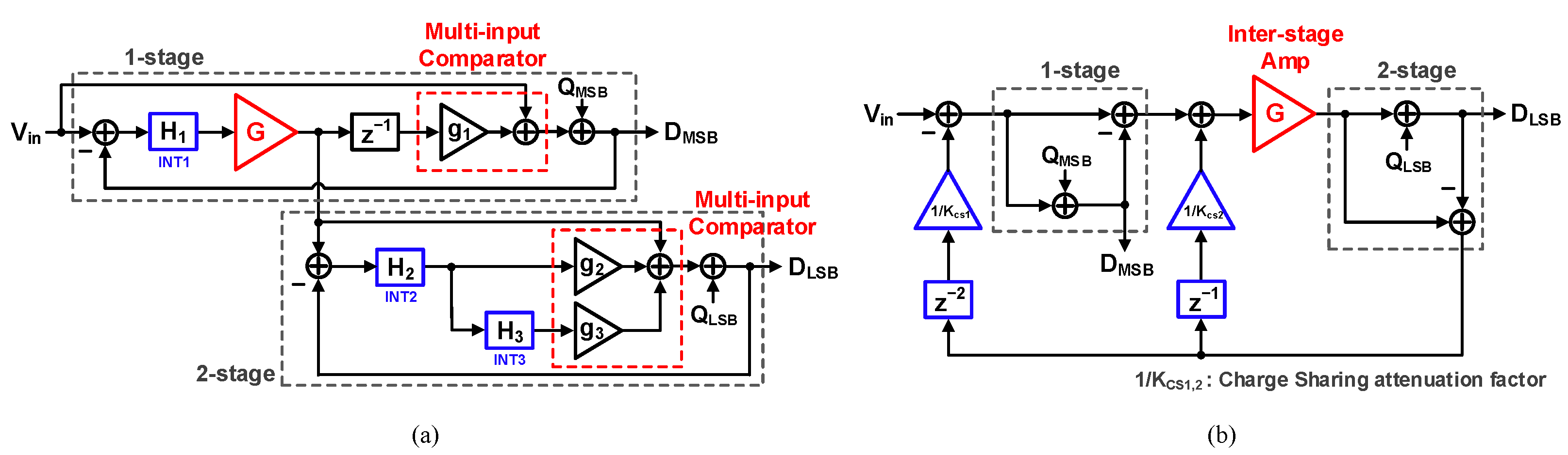
In hardware systems for Internet-of-Things (IoT) applications, it is preferred to use analog-to-digital converters (ADCs) with high resolution and energy efficiency in bands ranging from a few MHz to tens of MHz. Successive approximation register (SAR) ADCs are often used in systems where energy efficiency is critical because they have very low power consumption. However, a SAR ADC is limited when it comes to obtaining high resolution, due to the settling error of capacitive digital-to-analog converter (CDAC) and comparator noise. Limitations also arise in the conversion speed, due to the sequential conversion of binary search and settling speed of CDAC. For better accuracy, a noise-shaping SAR (NS-SAR) ADC, which combines a SAR ADC and delta-sigma ADC, is introduced for both high energy efficiency and accuracy [1,2]. However, speed and resolution limitations due to the SAR operation-based conversion and comparator noise persist. To address these issues, [3] proposed a pipelined noise-shaping SAR (PLNS-SAR) ADC that incorporates the pipelined ADC structure into the NS-SAR ADC. Slow SAR conversion can be pipelined in two stages to increase the overall operation speed. Moreover, the inter-stage amplifier can suppress the comparator noise, compared to the quantization noise, thus significantly reducing its impact. However, using an inter-stage amplifier, which is essential for pipelined architecture, increases the overall power consumption, consequently reducing the energy efficiency of ADC. As illustrated in [3], operational amplifiers cause significant energy losses, due to the static current. In the pipeline structure, the speed of the operational amplifier is very important because the speed of ADC is not only governed by the conversion time but also by the time during which the residual voltage is amplified by the amplifier. The use of operational amplifiers in pipelined NS-SAR ADCs is undesirable because operational amplifiers with wide bandwidth eventually require more power consumption. As an alternative, a pipelined NS-SAR ADC using a ring amplifier was proposed in [4]. Due to its inverter-based operation, the ring amplifier is a structure that can satisfy both low power consumption and high operating speed. As a result, [4] achieved less power consumption with the same third-order structure to [3] by replacing the amplifier. Although reducing the power consumption, [4] required multi-input comparators for residue voltage summation because the conventional cascaded integrator feed-forward (CIFF) structure was applied. The additional input pair of comparator causes additional noise and mismatches, thus deteriorating the performance of NS-SAR ADC. In practice, [4] was implemented as a structure with a third-order NTF. However, it had a somewhat lower SNDR.
Figure 1a shows a PLNS-SAR ADC based on the previous CIFF structure. Both the first and second stages used multi-input comparators because of the residue voltage summation. In addition, the gain of multi-input comparators was utilized to compensate for the attenuation occurring from charging sharing for integration. The comparator gain easily changes, due to the variation of the comparator input devices. The comparator gain variation of the second-stage significantly changes the NTF, thus reducing the performance of system. The structure in Figure 1a is based on a 1–2 MASH structure, where the second-order NTF from the second-stage was , thus making it impossible to obtain a sharper NTF notch in the CIFF structure using a passive integrator, ultimately limiting the achievable resolution.
In this paper, we presented a second-order PLNS-SAR ADC implemented in an error-feedback (EF) structure, instead of a CIFF structure. Figure 1b shows the proposed EF structure. This structure has an NTF of , which can obtain an NTF with a sharper notch in the second stage. Moreover, it does not depend on a comparator gain because of the inter-stage gain, G, which compensates for the charge sharing attenuation, , occurring during signal processing. Additionally, since feedback errors are summated by charge sharing, we do not have to use a multi-input comparator. Thanks to this, the proposed structure uses single-input comparators in both the first and second stages. Additionally, the conventional EF structure often uses a separate amplifier that compensates for charge sharing attenuation, even though it is not implemented in a pipelined structure [5]. In the proposed structure, the feedback error is amplified by reusing the inter-stage amplifier for the amplification of the quantization error of the first stage of the pipelined ADC. This eliminates the need for a separate amplifier for error feedback, thus minimizing power consumption and achieving high resolution.
2. Architecture
Figure 2 shows the block diagram of the proposed PLNS-SAR ADC. There are two stages, based on the SAR ADC, and an inter-stage amplifier between them. The quantization error of the second stage becomes an EF signal through the FIR filter, which is summated at the input terminal of each stage. A passive switched capacitor (SC)-based FIR filter is used for simplicity and low power consumption. It consists of a delay and attenuation, occurring during charge sharing, that transfers the quantization error from the second stage to other capacitors. The feedback error delivered to the first stage is delayed by two samples (), which can be simply implemented using the natural timing difference between the first and second stages in the pipeline structure. In the proposed pipelined structure, the quantization error from the second stage is transferred to the first stage, where the input after two sampling periods is sampled. On the other hand, the feedback error delivered to the second stage is delayed by one sample (). The desired delay occurs when the quantization error generated in the second stage is added to the input of the inter-stage amplifier, before starting the next conversion in the second stage. The feedback error of each stage is stored in the capacitor. For the first stage, the feedback error can be summated with the input signal sampled on the CDAC of the first stage (CDAC1) through charge sharing, before starting the SAR conversion, which causes another attenuation by , in addition to the original attenuation by . However, this does not significantly affect the resolution because it can be compensated by the subsequent inter-stage gain. For the second stage, additional attenuation occurs similarly if the feedback error that is already attenuated by is added directly to CDAC of the second stage (CDAC2), which makes it difficult to obtain the desired NTF because this loss is not compensated by the inter-stage gain. Therefore, the feedback error is fed to the amplifier’s input, together with CDAC1, when the inter-stage amplifier starts amplifying right after finishing the first-stage conversion, in order to prevent attenuation (details on timing are covered in Section 3.1). In this case, we can easily obtain the desired NTF because the feedback error is amplified by the inter-stage gain, similar to that in the first stage. Therefore, the feedback error can easily be handled without a multi-input comparator or additional amplifier. Moreover, the SAR quantizer in each stage can be simply implemented using a single-input comparator. Additionally, the attenuation by , due to charge sharing, is compensated by the inter-stage amplifier, which is another major advantage.
The final output () and output of each stage in Figure 2 are obtained as follows. First, the digital output of the first stage () is expressed as Equation (1).
The residue voltage of the first stage (), generated by subtracting from Vin being reflected through CDAC, is expressed as:
Then, is amplified by G via amplifier after adding and feedback error.
As a result, the Equation (4) can be obtained through the digital filter and digital final output is as follows:
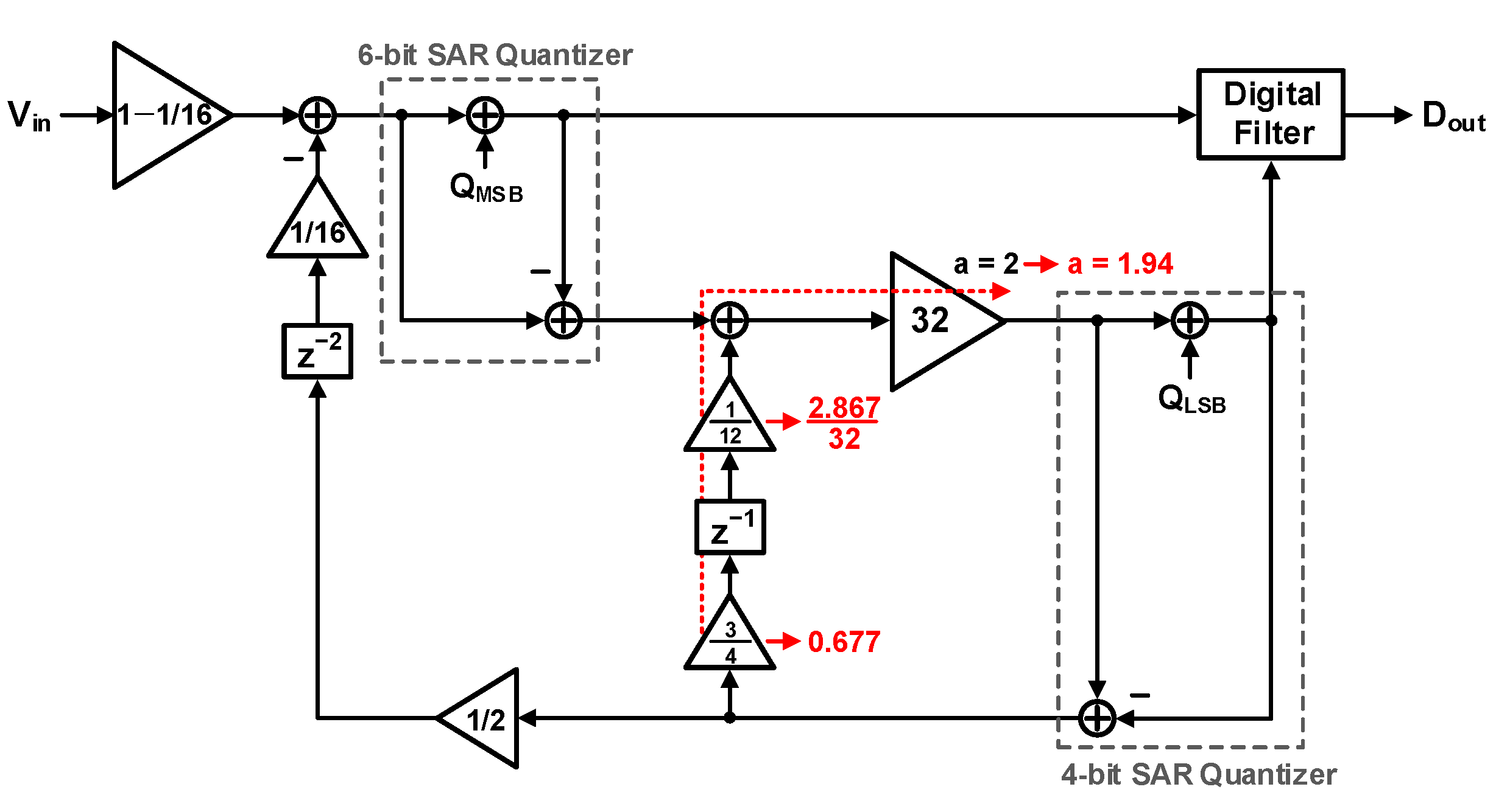
The outputs of the two stages go through the digital cancellation filter, shown in Figure 2, to produce the final digital output signal,. The proposed PLNS-SAR ADC structure maintains the advantages of the pipelined structure, along with the second-order noise-shaping. The second-stage output, , is multiplied by the inter-stage gain reciprocal and added to the first-stage output, which ideally cancels the first-stage quantization () and comparator noise (), while leaving only the noise related to the second stage. After digital cancellation, is expressed as Equation (5). The transfer function in Equation (6) can be obtained through additional coefficient adjustment. At this time, the NTF becomes . For this, which is the coefficient of the second-order term of the NTF in Equation (5), should be in unity. That means that should be the inter-stage gain, G. We can easily implement this by adjusting the ratio of the capacitors used for charge sharing to store the second-stage quantization error and charge sharing capacitor ratio for error feedback at the first-stage input. When the coefficient of the second-order term is set to unity, the zeros of the NTF are , where . Thus, we can adjust G or to move the zero position and achieve the target NTF. The inter-stage gain cannot be accessibly changed; thus, it is easier to change the charge sharing capacitor ratio, . When a = 2, the zero is located at 1, and a general second-order high pass NTF of is obtained. Depending on the target oversampling ratio (OSR), the zero can be moved from ), and the in-band noise can be minimized [6]. As a result, the second-stage quantization noise () and comparator noise () shown in the output become shaped by the second order. In addition, the noise is also attenuated by G, as shown in Equation (6), which helps to obtain high resolution.
Figure 3 is the block diagram reflecting the practical circuit implementation of the proposed ADC structure. As mentioned earlier, the charge sharing capacitor ratio and G determine the NTF. Additionally, G is involved in the allocation of bits between the pipelined stages. The noise requirement for the second-stage significantly increases with the decrease in G. Additionally, relatively small is required, resulting in large input signal attenuation and, consequently, reducing the dynamic range of the ADC. To balance the first and second stages and minimize the dynamic range loss, we set G to 32. The first stage converts six bits, excluding redundancy, and the second stage converts four bits. To generate the feedback error to the first stage from the second-stage quantization error, charge sharing that causes attenuation (= 2) is essential. The feedback error with this attenuation by two becomes attenuated again when it is summated with Vin through charge sharing. At this time, the charge sharing ratio is set to 16(=), so that the loop gain for the feedback error, including the inter-stage gain, is in unity. The input signal also becomes 15/16 times, due to this charge sharing, thus slightly decreasing the dynamic range of the ADC. There is a loss of −1.6 dB in the dynamic range, but this is not significant, considering the improved SNDR of the ADC. For the second stage, the attenuation, , needs be 16 to achieve a = 2. This implies that the transmitted feedback error via charge sharing is very small, which deteriorates the noise performance. Therefore, is set to a much smaller value of 4/3. Additionally, to maintain the loop gain of the feedback error to the second-stage the same, the feedback capacitor ratio for the inter-stage amplifier is changed for amplification of the feedback error by 8/3. This does not change the gain of 32 for the first-stage quantization error, since the amplifier has multi-path inputs. Figure 4a shows the simulated output power spectral density of the final output, when the zero is located at z = 1. The second-order noise-shaping is applied to 10-bit conversion, without zero optimization, showing an ideal SNDR of 81.95 dB when the OSR is 7. We applied zero optimization to obtain a higher SNDR than the frequently used second-order NTF of . We set a to 1.94. To this end, the value at which the feedback error is amplified changed from 8/3 to 2.867. Figure 4b shows the simulated output power spectral density after zero optimization. It is observed that the SNDR increases by about 4.2dB, without any additional power consumption. Consequently, the proposed ADC can achieve an ENOB of up to 14 bits.
3. Circuit Implementation
3.1. Pipelined Noise-Shaping SAR ADC
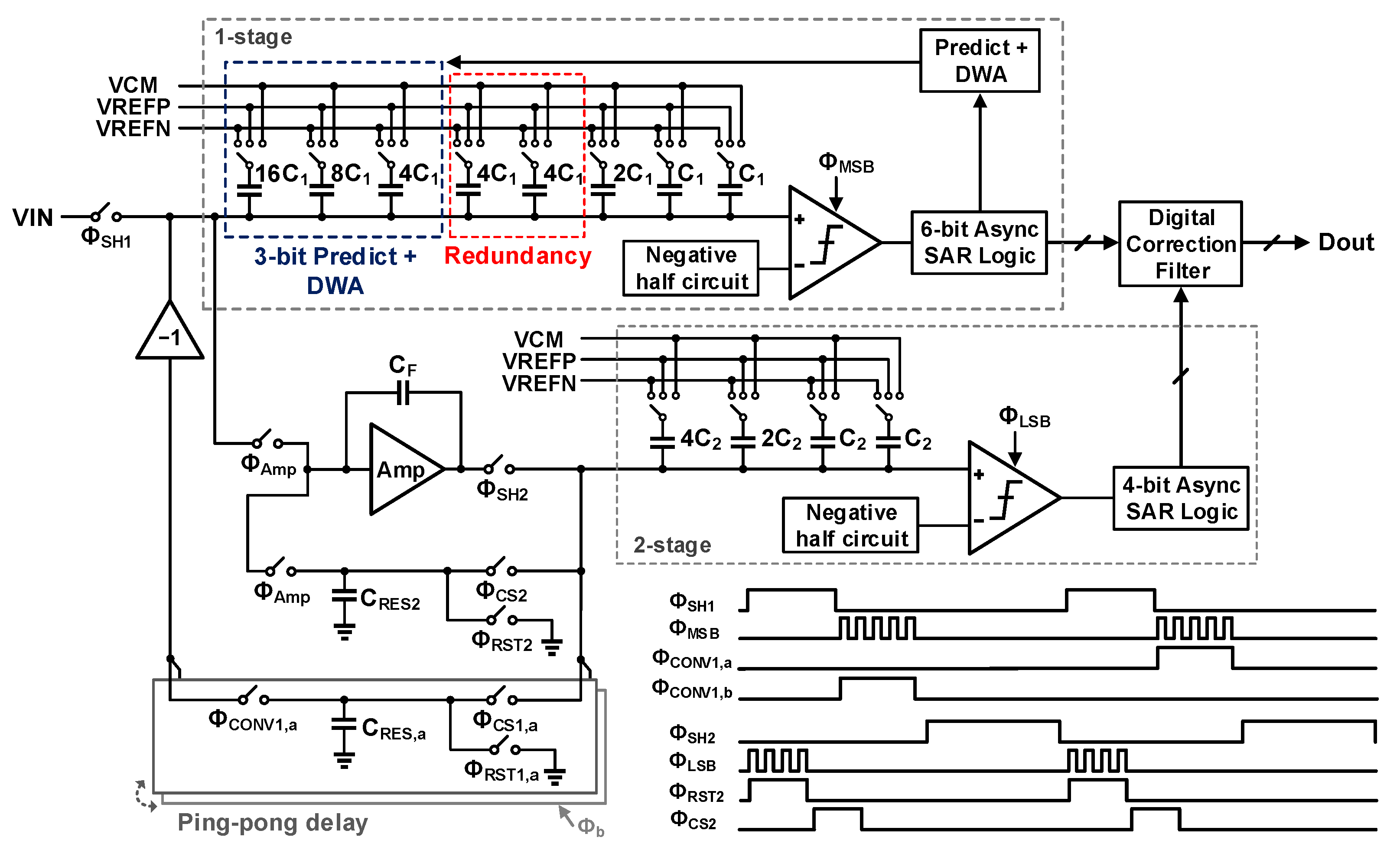
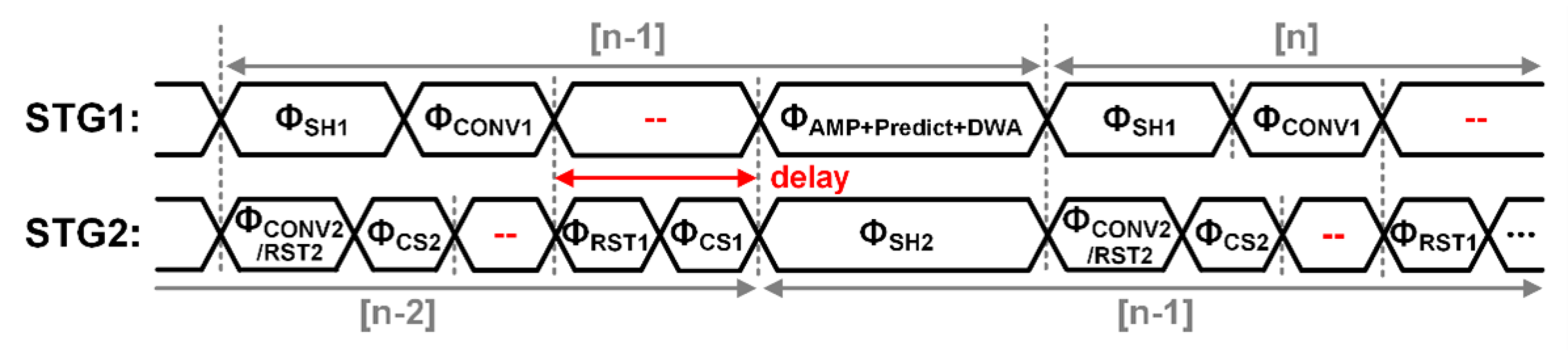
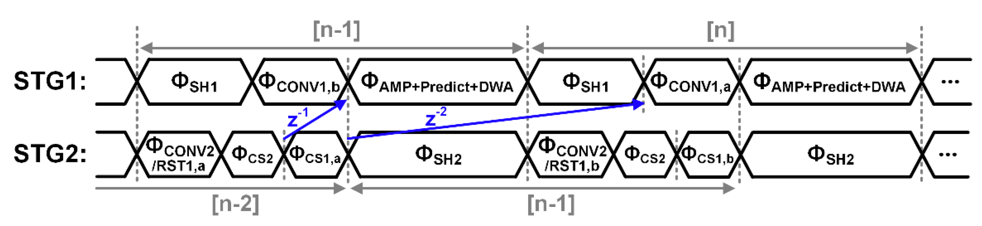
Figure 5 shows circuit implementation of the proposed ADC. First, an input signal is sampled at the first stage (), and then a 6-bit conversion is performed (). Despite having a conversion result of six bits, the actual conversion consists of five cycles. With the results of the previous conversion, the three most significant nits (MSBs) are predicted and reflected in the CDAC1. To correct for the prediction error, 2-bit redundant conversion is performed. After that, the remaining 3-bit conversion is performed. Further details on performing the prediction are mentioned in Section 3.2. The array of CDAC1 is configured according to this conversion method, and a tri-state switching method [7] is used to maintain a constant input common-mode voltage of the inter-stage amplifier, thus achieving constant performance. When the conversion is finished in the first stage, the quantization error remaining on CDAC1 and feedback error on are added at the input of the inter-stage amplifier and amplified (). The amplified voltage is then sampled on CDAC2 in the second stage (). Once the conversion starts in the second stage after the sampling, the voltage on is no longer necessary, so it becomes reset. After the conversion in the second stage is finished, the remaining quantization error on CDAC2 is charge-shared with both and to generate the feedback error. The charge sharing is first performed with , which is ready after being reset (). Then, before the second charge sharing with starts, needs to be reset; however, since is in use during the conversion of the first stage, it should be reset after the conversion of the first stage. Therefore, must come right after . Once the reset is completed, follows (Figure 6). In other words, the amplification phase ( or ) cannot start immediately after , thus leading to delay. Similarly to the second-stage, a delay takes place after . Due to this inefficient operation timing, the overall speed decreases. To address this issue, this work optimizes the operation timing by alternately using two sets of and speeds up the overall ADC speed. Figure 7 shows the final timing diagram used by the proposed structure. Because there are two sets of , while one of them is used for the first stage, the other can be reset. Thus, the delay disappears and the overall operating speed increases. After , can start without any delay. At this time of amplification, the logic for dynamic weight averaging (DWA) and prediction logic, using the previous conversion results, operate without causing any timing overhead.
The total capacitance of CDAC1 in the first stage is 1.6 pF, considering the thermal noise of kT/C. The feedback capacitor of the amplifier, , is set to 50 fF for the gain of 32. The total capacitance of CDAC2 in the second stage is 300 fF. The remaining voltage, Vqn2, after conversion on CDAC2 is first charge shared with . Here, the voltage becomes Vqn2 . This voltage is then fed back to the input terminal of the inter-stage amplifier and amplified by . Therefore, the loop gain for Vqn2 in the second-stage becomes , and the size of is determined to be 143.35 fF for the desired value (=1.94). For , the charge sharing occurs with the gain of . Then, it is fed back to CDAC1 with the gain of during . Accordingly, the size of is determined to be 107 fF. Note that the minus sign of the gain for to CDAC1 shown in Figure 5 can be simply implemented using the differential circuit characteristic.
3.2. Prediction and DWA
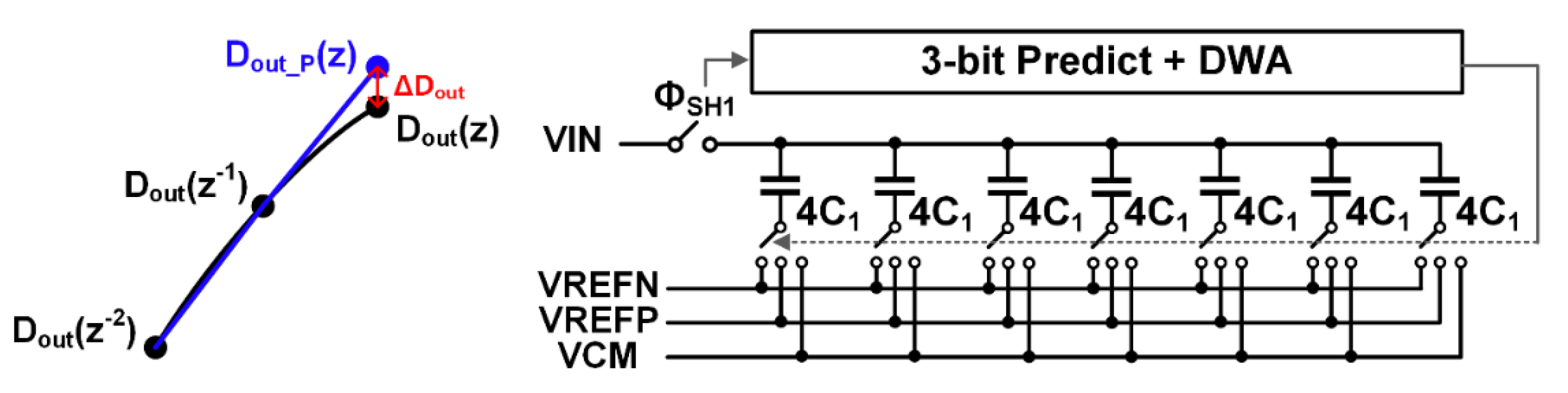
In CDAC1, the mismatch between unit capacitors is one of the main factors limiting the high SNDR of ADCs. That is because it generates data-dependent non-linearity. There is also unit capacitor mismatch in CDAC2. However, since its effect is attenuated by the inter-stage gain in the pipeline structure, we can ignore it. Therefore, a high SNDR cannot be achieved, even when using the proposed ADC structure, unless we calibrate the mismatch between the unit capacitors in CDAC1 (even though the first stage has a small number of bits). DWA is a popular method used to suppress in-band tones by shaping the mismatch between unit capacitors in noise-shaping-based, high-resolution ADCs. A plain DWA method is used for CDAC1 in this work, and the error due to the unit capacitor mismatch is shaped in the first-order high pass type [8]. Since the signal band exists in the low-frequency region, it is possible to attenuate the harmonic within the band. However, applying the DWA to all six bits of the first stage leads to complicated logic and slow operating speed. DWA, for only three MSBs introduced in [9], was applied to this work because the unit capacitor mismatch is adequately shaped to have a minor effect on realizing the target SNDR with only that method. Accordingly, a capacitor array consisting of three MSBs [16C 8C 4C] in the CDAC1 of the first stage, as shown in Figure 8 (right), is split into seven identical units, with sizes of 4C. According to the DWA logic results, seven capacitor units in the CDAC1 are selectively switched to enable unit capacitor mismatch shaping. However, for the DWA logic to function, three MSBs obtained from the current input signal are essential. To obtain this pre-decision result, a method for converting the required number of MSBs using a separate coarse ADC before performing the main SAR conversion is often used; the method is shown in [10]. However, using a separate coarse ADC leads to an offset problem or increase in total input capacitance [11]. Therefore, in the proposed structure, the pre-decision results required for the DWA operation are obtained without separately using the coarse ADC, namely via the prediction algorithm. The prediction algorithm does not suffer from problems in the analog domain because it handles signals in a fully digital way [12], thus allowing it to predict current data using previous data, which is shown in Figure 8 (left). Additionally, since the 3-bit MSB conversion time is not separately required, we can increase the operation speed of the first stage. Therefore, the prediction and DWA logic do not affect the speed of the ADC. That is because the data required for the next conversion are calculated in advance during the amplification phase ().
The prediction algorithm of the proposed structure is the second-order prediction, and the prediction method is expressed in Equation (3). The calculated value is transferred to the DWA logic, and the seven capacitors in the array are switched according to the result. The (z) calculated from the previous two samples can have a significantly large error, compared to (z), which is obtained from the accurate conversion. Even if the error is assumed to be small, the performance degradation can be huge, considering the proposed ADC target’s high-resolution. However, since the proposed ADC oversamples, the frequency region of the input signal is relatively low, compared to the sampling frequency. Thus, the error would be limited, even if we apply the prediction algorithm. Furthermore, we can eliminate the bounded error via the 2-bit redundant conversion before the SAR conversion starts and after applying the output value of DWA logic. As shown in CDAC1 in Figure 5, the redundancy of 4C size is applied twice, compensating for a total of 128 LSB size prediction errors.
3.3. Ring Amplifier
Existing NS-SAR ADCs, without using the pipelined structure, use a high gain multi-input comparator to compensate for the integration loss and obtain the desired NTF [13]. The high gain multi-input comparator has a large design overhead, due to the large kickback noise and power consumption. In this work, only single-input comparators are used, so the NTF is insensitive to a parasitic. For the use of single-input comparators, the inter-stage amplifier is utilized for error feedback. The amplifier used in the proposed structure is the ring amplifier shown in Figure 9 [4]. The three inverters are cascaded to obtain a high gain, and the last inverter operates in a slew mode at the beginning of amplification. After settling, it operates in the sub-threshold region, thus optimizing power consumption. Since the amplifier is not always in operation, the ring amplifier does not consume power in the non-amplification phase, thus increasing the overall power efficiency. It operates as a switched-capacitor amplifier with a constant gain, as shown in Figure 9, where the capacitive feedback is configured around the ring amplifier. The operation of the amplifier is as follows: the feedback capacitor is only used for the amplification phase (), so it is reset during the non-amplification phase (). At the input of the amplifier, two capacitors are connected via a switch; one is CDAC1 containing a quantization error of the first stage, and the other is with a feedback error. During the amplification phase, the charge in the two capacitors moves to and each voltage is simultaneously added and amplified to appear as an output voltage. At this time, CDAC2 is connected to the ring amplifier as a load, and the amplified voltage is sampled on CDAC2. The inter-stage gain by the switched-capacitor amplifier is and error feedback gain is , which are set to 32 and 2.867, respectively, as mentioned above. Both values affect the first-order term coefficient of the NTF. When the gain has any variation or error, the NTF zero moves, and the achievable resolution decreases. Therefore, the calibration circuit is added to change the capacitance of to counter the large variation, thus allowing for the formulation of the desired zero. Although CDAC1 cannot counter the gain change, due to its difficult calibration, the error can be compensated for by calibrating the digital cancellation filter coefficient.
Figure 10 demonstrates the SNDR distribution, according to the variation in the gain of amplifier. Figure 10a shows the obtained SNDR distribution when the amplifier’s gain (=32) changes by 5%. For 5% gain variation, the SNDR changes from 70 to 90 dB. Figure 10b exhibits the result after calibrating the coefficient of the digital cancellation filter. Even if the inter-stage gain changes by 5%, the calibration of the filter coefficient can maintain the SNDR between 83 and 91 dB. The coefficient of the digital cancellation filter can be adjusted off the chip, together with the gain of amplifier. Therefore, the proposed structure is robust to the gain variation of the amplifier, which makes a high-performance amplifier unnecessary.
4. Results
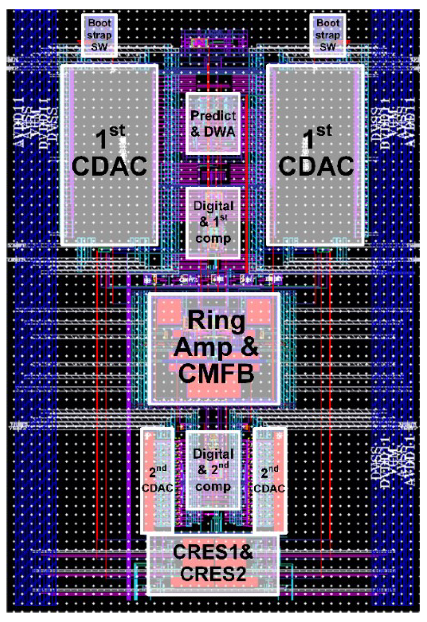
The proposed PLNS-SAR ADC is designed using a 28 nm CMOS process. Figure 11 shows the layout of the ADC core. The total core area is 167 × 320 um, and it is occupied by the SAR ADCs for the two stages, ring amplifier, and error feedback capacitors. For , the same unit capacitor used for the CDAC was used to suppress any mismatch.
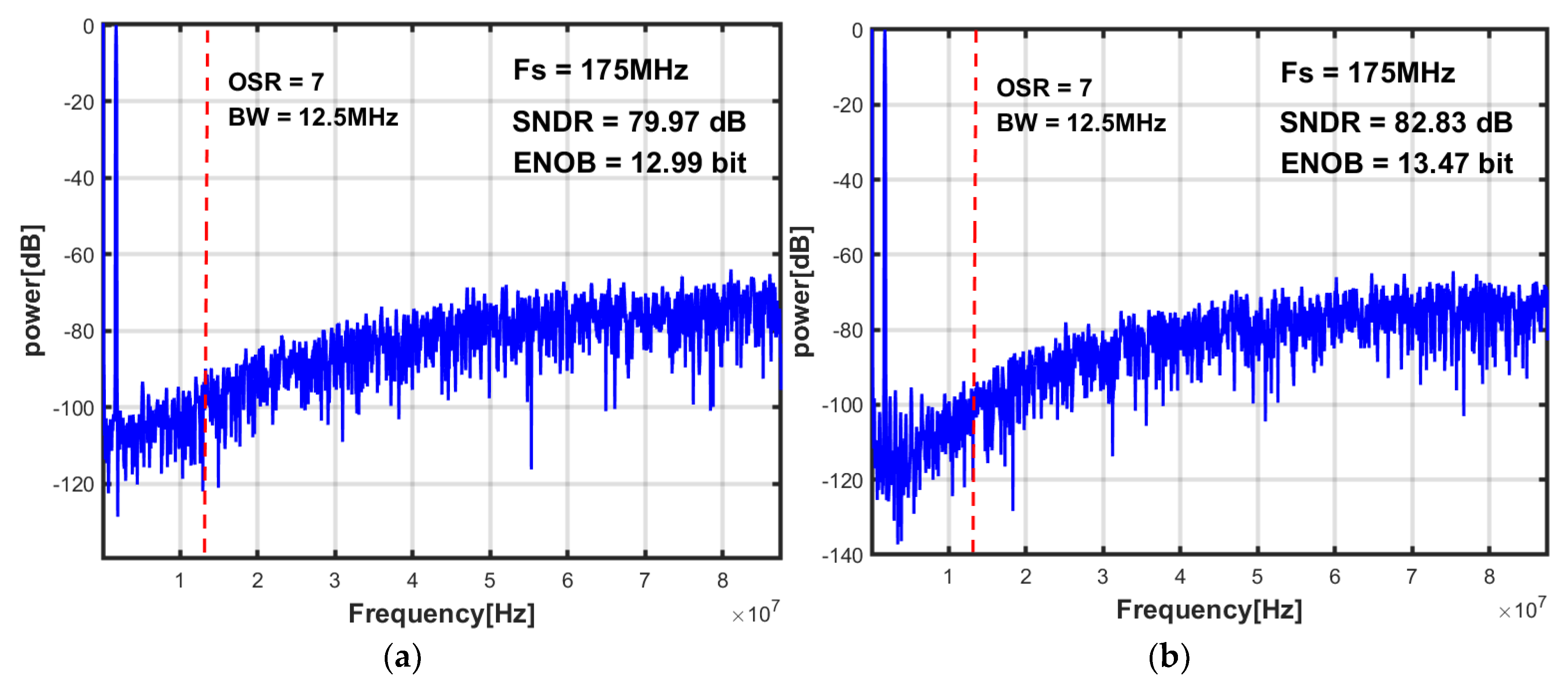
Figure 12a shows the output power spectral density from the simulation, with transient noise reaching up to 20 GHz. Figure 12b shows the result from post-layout simulation after parasitic extraction. The simulation is performed in a typical process corner at a room temperature of 27 °C. The input signal has a 1.7-MHz frequency and magnitude of −0.9 dBFS. The digital outputs from the first and second stages are processed by a digital cancellation filter off the chip by using MATLAB. The filtered data achieves a 12.5-MHz BW and 79.97-dB SNDR, at a 175-MHz sampling frequency, with OSR of 7. Figure 13 shows the total power consumption and power breakdown for each block for the 175-MHz sampling frequency. The total power consumption of the proposed ADC is 4.27 mW at a 1.1-V supply voltage. The most power-hungry block is the ring amplifier, and it consumes 1.75 mW. The energy efficiency is improved, compared to [3], using an OTA for the inter-stage amplifier, while the speed is increased. The digital blocks consume a total of 1.58 mW, but the prediction and DWA logic account for only 0.15 mW, without deteriorating the Schreier figure-of-merit (FoMs) of the proposed ADC. The SNDR, BW, and power consumption from the simulation results demonstrate that the proposed structure provides a good FoMs of 174.6 dB. In other process corner simulations, the maximum sampling rate differs (slow: 160 MHz, typical: 175 MHz, and fast: 189 MHz), but the maximum SNDR barely changes.
Table 1 compares the proposed ADC with previous works. Since many external factors might be excluded in the post-layout simulation results from this work, there might be a significant difference for actual measurements. However, it is still meaningful to compare the proposed EF PLNS-SAR ADC with the PLNS-SAR ADC, based on the existing CIFF structure, under the same simulation environment. The proposed structure is advantageous for achieving a higher SNDR than the prior ones; it can have a higher sampling rate and wider bandwidth.
5. Conclusions
In this paper, we propose a PLNS-SAR ADC capable of achieving a high sampling rate and resolution. The EF-based second-order NS ADC is implemented on the structure of a pipelined SAR ADC, while maintaining its advantages. The power efficiency is enhanced by reusing the inter-stage amplifier, which is essential in the two-stage pipelined SAR ADC, for processing the feedback error voltage. Due to the digital cancellation filter and capacitor calibration, it is possible to obtain a constant resolution in the existence of the amplifier’s gain variation. The prediction and DWA logic enhance the speed and resolution of the ADC. The prediction could reduce the number of conversion cycles by three. Additionally, the speed of the ADC can be optimized by alternating the error feedback capacitor. The SNDR is further improved by zero optimization. Accordingly, the proposed PLNS-SAR ADC achieves high energy efficiency and improves the resolution and bandwidth.
Author Contributions
Conceptualization, J.B., J.L. and H.C.; methodology, J.B.; software, J.B. and J.L.; validation, J.B.; formal analysis, J.L.; investigation, J.B. and J.L.; resources, H.C.; data curation, J.B. and J.L.; writing—original draft preparation, J.B.; writing—review and editing, J.B. and H.C.; visualization, J.B. and J.L.; supervision, J.B. and H.C.; project administration, H.C. and J.K.; funding acquisition, H.C. All authors have read and agreed to the published version of the manuscript.
Funding
This research was funded by the National Research Foundation of Korea, grant number 2020R1A2C1099786.
Conflicts of Interest
The authors declare no conflict of interest.
References
- Fredenburg, J.A.; Flynn, M.P. A 90-MS/s 11-MHz-Bandwidth 62-dB SNDR Noise-Shaping SAR ADC. IEEE J. Solid-State Circuits 2012, 47, 2898–2904. [Google Scholar] [CrossRef]
- Guo, W.; Sun, N. A 12b-ENOB 61µW noise-shaping SAR ADC with a passive integrator. In Proceedings of the ESSCIRC Conference 2016: 42nd European Solid-State Circuits Conference, Lausanne, Switzerland, 12–15 September 2016. [Google Scholar]
- Oh, S.; Oh, Y.; Lee, J.; Kim, K.; Lee, S.; Kim, J.; Chae, H. A 85 dB DR 4 MHz BW pipelined noise-shaping SAR ADC with 1–2 MASH structure. IEEE J. Solid State Circuits 2021, 56, 3424–3433. [Google Scholar] [CrossRef]
- Lee, J.; Lee, S.; Kim, K.; Chae, H. A Pipelined Noise-Shaping SAR ADC Using Ring Amplifier. Electronics 2021, 10, 1968. [Google Scholar] [CrossRef]
- Li, S.; Qiao, B.; Gandara, M.; Pan, D.Z.; Sun, N. A 13-ENOB Second-Order Noise-Shaping SAR ADC Realizing Optimized NTF Zeros Using the Error-Feedback Structure. IEEE J. Solid-State Circuits 2018, 53, 3484–3496. [Google Scholar] [CrossRef]
- Pavan, S.; Schreier, R.; Temes, G.C. Understanding Delta-Sigma Data Converters, 2nd ed.; IEEE: Piscataway, NJ, USA, 2017. [Google Scholar]
- Hariprasath, V. Merged capacitor switching based SAR ADC with highest switching energy-efficiency. Electron. Lett. 2010, 46, 620. [Google Scholar] [CrossRef]
- Neitola, M.; Rahkonen, T. A Generalized Data-Weighted Averaging Algorithm. IEEE Trans. Circuits Syst. II Express Briefs 2010, 57, 115–119. [Google Scholar] [CrossRef]
- Zhou, X.; Gui, X.; Gusev, M.; Ackovska, N.; Zhang, Y.; Geng, L. A 12-Bit 20-kS/s 640-nW SAR ADC with a VCDL-Based Open-Loop Time-Domain Comparator. IEEE Trans. Circuits Syst. II Express Briefs 2022, 69, 359–363. [Google Scholar] [CrossRef]
- Shu, Y.-S.; Kuo, L.-T.; Lo, T.-Y. An Oversampling SAR ADC with DAC Mismatch Error Shaping Achieving 105 dB SFDR and 101 dB SNDR Over 1 kHz BW in 55 nm CMOS. IEEE J. Solid-State Circuits 2016, 51, 2928–2940. [Google Scholar] [CrossRef]
- Tai, H.; Hu, Y.; Chen, H. A 0.85fJ/conversion-step 10b 200kS/s subranging SAR ADC in 40nm CMOS. In Proceedings of the IEEE International Solid-State Circuits Conference Digest of Technical Papers (ISSCC), San Francisco, CA, USA, 9–13 February 2014. [Google Scholar]
- Shakya, J.R.; Vadakkan, A.K.; Temes, G.C. Predictive Noise Shaping SAR ADC. In Proceedings of the IEEE International Symposium on Circuits and Systems (ISCAS), Sapporo, Japan, 26–29 May 2019. [Google Scholar]
- Liu, J.; Li, S.; Guo, W.; Wen, G.; Sun, N. A 0.029-mm2 17-fJ/Conversion-Step Third-Order CT ΔΣ ADC with a Single OTA and Second-Order Noise-Shaping SAR Quantizer. IEEE J. Solid-State Circuits 2019, 54, 428–440. [Google Scholar]
- Hsu, C. A 77.1-dB 6.25-MHz-BW Pipeline SAR ADC with Enhanced Interstage Gain Error Shaping and Quantization Error Shaping. In Proceedings of the IEEE Custom Integrated Circuits Conference (CICC), Boston, MA, USA, 22–25 March 2020. [Google Scholar]
- Yi, P.; Liang, Y.; Liu, S.; Xu, N.; Fang, L.; Hao, Y. A 625kHz-BW, 79.3dB-SNDR Second-Order Noise-Shaping SAR ADC Using High-Efficiency Error-Feedback Structure. IEEE Trans. Circuits Syst. II Express Briefs 2022, 69, 859–863. [Google Scholar] [CrossRef]
Figure 1.
(a) Conventional CIFF structure. (b) Proposed EF Structure for PLNS-SAR ADC.

Figure 2.
Detailed block diagram of proposed ADC architecture.

Figure 3.
Block diagram for practical circuit implementation.

Figure 4.
Power spectral density (a), with zero located at 1 (b) with zero optimization.

Figure 5.
Circuit implementation of proposed PLNS-SAR ADC.

Figure 6.
Inefficient ADC operation, due to delays.

Figure 7.
Final timing diagram of proposed structure without any delay.

Figure 8.
(left) Second-order prediction algorithm; (right) CDAC configuration for 3-bit DWA application.
Figure 8.
(left) Second-order prediction algorithm; (right) CDAC configuration for 3-bit DWA application.

Figure 9.
Structure of ring amplifier and multi-input inter-stage amplifier based on ring amplifier.
Figure 9.
Structure of ring amplifier and multi-input inter-stage amplifier based on ring amplifier.

Figure 10.
SNDR distribution by amplifier gain variation (a) before and (b) after digital filter calibration.
Figure 10.
SNDR distribution by amplifier gain variation (a) before and (b) after digital filter calibration.

Figure 11.
Proposed ADC core layout.

Figure 12.
Simulated output power spectral density: (a) noise included; (b) RC-extraction included.

Figure 13.
Power breakdown of proposed ADC.


Table 1.
Comparison table.
| [3] | [4] | [14] | [5] | [15] | This Work | |
|---|---|---|---|---|---|---|
| Architecture | Pipelined NS-SAR | Pipelined NS-SAR | Pipelined NS-SAR | NS-SAR | NS-SAR | Pipelined NS-SAR |
| Structure | CIFF | CIFF | CIFF-DEF | EF | EF | EF |
| Technology | 65 nm | 65 nm | 40 nm | 40 nm | 65 nm | 28 nm |
| Fs [MHz] | 83.3 | 72 | 100 | 10 | 20 | 175 |
| BW [MHz] | 4.1 | 5.15 | 6.25 | 0.625 | 0.625 | 12.5 |
| OSR | 10 | 7 | 8 | 8 | 16 | 7 |
| Resolution [bit] | 8 | 9 | 11 | 9 | 9 | 10 |
| Supply [V] | 1.2 | 1.2 | 1 | 1.1 | 1.2 | 1.1 |
| SNDR [dB] | 78.2 | 70 | 77.1 | 79 | 79.3 | 79.9 |
| Power [mW] | 3.5 | 2.4 | 1.38 | 0.084 | 0.113 | 4.27 |
| FoMs [dB] | 168.8 | 163.5 | 173.7 | 178 | 176.7 | 174.6 |
| Area [mm2] | 0.113 | 0.099 | 0.054 | 0.024 | 0.354 | 0.053 |
| Measurement | Experiment | Experiment | Experiment | Experiment | Experiment | simulation |
.
Publisher’s Note: MDPI stays neutral with regard to jurisdictional claims in published maps and institutional affiliations. |
© 2022 by the authors. Licensee MDPI, Basel, Switzerland. This article is an open access article distributed under the terms and conditions of the Creative Commons Attribution (CC BY) license (https://creativecommons.org/licenses/by/4.0/).
Share and Cite
MDPI and ACS Style
Baek, J.; Lee, J.; Kim, J.; Chae, H. 2nd-Order Pipelined Noise-Shaping SAR ADC Using Error-Feedback Structure. Electronics 2022, 11, 3072. https://doi.org/10.3390/electronics11193072
AMA Style
Baek J, Lee J, Kim J, Chae H. 2nd-Order Pipelined Noise-Shaping SAR ADC Using Error-Feedback Structure. Electronics. 2022; 11(19):3072. https://doi.org/10.3390/electronics11193072
Chicago/Turabian StyleBaek, Jihyun, Juyong Lee, Jintae Kim, and Hyungil Chae. 2022. "2nd-Order Pipelined Noise-Shaping SAR ADC Using Error-Feedback Structure" Electronics 11, no. 19: 3072. https://doi.org/10.3390/electronics11193072
Note that from the first issue of 2016, this journal uses article numbers instead of page numbers. See further details here.