
A Multimodal Modulation Scheme for Electric Vehicles’ Wireless Power Transfer Systems, Based on Secondary Impedance

1
ZXNE Corporation, Shenzhen 518101, China
2
School of Automotive and Transportation Engineering, Shenzhen Polytechnic, Shenzhen 518055, China
*
Author to whom correspondence should be addressed.
Electronics 2022, 11(19), 3055; https://doi.org/10.3390/electronics11193055
Submission received: 3 August 2022
/
Revised: 21 September 2022
/
Accepted: 22 September 2022
/
Published: 25 September 2022
(This article belongs to the Special Issue Wireless Power Transfer and Wireless Energy Harvest)
Abstract
:This study aimed to investigate a multimodal modulation scheme that takes into account the wide range of output characteristics, numerous constraints, and complex working conditions in the wireless charging of electric vehicles. Key electrical parameters and variables in the secondary stages of electric vehicle wireless power transfer (EV-WPT) systems were evaluated based on capacitive, inductive, and resistive impedance working modes. The limiting duty cycle values, D, of the rectifier were derived by detecting the mutual inductance, M. This multimodal modulation was adopted, based on the secondary equivalent impedance phase, to control the impedance working condition and, hence, achieve optimal working performance. The proposed method can modulate the system performance before and during wireless transmission. The proposed control scheme was verified using a 10 kW EV-WPT experimental prototype under a capacitive impedance working mode with 8.5 kW power output. Our proposed method achieved full power output by modulating the impedance working conditions.
1. Introduction
In the past decade, many countries have endeavored to develop new energy vehicles (NEVs) to address the problems of tailpipe emissions, environmental deterioration, and energy challenges. The NEV industry has experienced explosive growth, particularly in electric vehicles (EVs). The development of intelligent connected vehicles controlled by electronics is an inevitable trend in the advancement of EVs. Currently, unmanned automatic parking systems are available in middle-end and high-end cars, while some of the models available offer an automated valet parking function. Unmanned and intelligent charging strategies are critical in improving the degree of automatization during the charging process because the charging of EVs is carried out when the vehicles are packed. Wireless power transfer (WPT) technology has matured into an important charging strategy for EVs since its initial development. Furthermore, wireless charging technology and its application in EVs is currently the focus of much academic and commercial research [1,2,3,4,5].
The public use of EVs’ wireless charging (EV-WPT) applications requires the implementation of the ground assembly (GA) charging function for all car models. Several charging classifications are defined in numerous international standards: IEC 61980 [6], ISO 19363 [7], SAE J2954 [8], and GB/T 38775 [9], as listed in Table 1.
The EVs’ wireless charging systems are characterized by a wide range of output characteristics, as shown in Table 1, which apply for all the above standards. For instance, the transmitting distance is covered under the gap requirement and has three different Z classifications, covering a minimum of 50 mm (Z1, 150 mm − 50 mm = 50 mm) and a maximum of 80 mm. For tolerance, 200 mm along the Y-axis and 150 mm along the X-axis is required. Moreover, the output voltage ranges between 300 and 450 V when the system is under full power output. A fixed working frequency is considered acceptable and is adopted in EV-WPT systems because there is a lack of radio service coexistence in most countries. Therefore, there is a need for system circuit topology and control strategies to solve the issues that we described earlier. The Series-Series (SS) topology is well-tuned here, but is associated with mistuned topologies, whereas the double-sided LCC compensation network is less sensitive to mistuning and is more suitable for EV-WPT applications [10]. Previous studies have proposed further research on an integrated coil design based on LCC compensation topology to improve the tolerance of front-to-rear and vertical misalignment [11]. In addition, the LCC-S-based discrete fast terminal sliding mode controller has been proposed to regulate the WPT system output current and power with optimal efficiency [12]. Furthermore, an optimal frequency-tracking method and online adjustment of the primary inverter duty ratio are proposed to achieve high efficiency and a high-power factor for the dynamic wireless power transfer system of EVs [13]. Frequency tracking is also provided to optimize the efficiency by tuning the inverter voltages [14]. Previous studies have also studied and optimized the output power in the EV-WPT system [15,16]. In a separate study, an adaptive smart control method for EV wireless charging has been proposed to shorten the wireless charging time of electric vehicles (EVs) and achieve stable charging [17]. It has been found that the majority of studies deal with the design and optimization of the charging process under one or several constraints. There are only a few studies that have simultaneously considered all the issues and addressed them in the same study.
This current study first analyzed the background and problems associated with EV charging systems. The optimum performance of the LCC-LCC EV-WPT system under three different impedance working modes was then analyzed. Moreover, this study also discussed the system performances and different key electrical characteristics under different impedance working modes. It was evident that the resistive working mode attained the maximum D range among the three different impedance working modes, whereas the D range under the capacitive working mode achieved the minimum values. Furthermore, D was calculated using the constraints Ie, Ip, Iin, and Uin, and the range values of D were different. In addition, a multi-modulation scheme was proposed in the current study, based on M detection and the phase angle of the secondary side. The duty cycle D of the rectifier was the criterion used to control the impedance working mode. Finally, this study ends with our conclusions.
2. Circuit Analysis
2.1. Circuit Working Principle
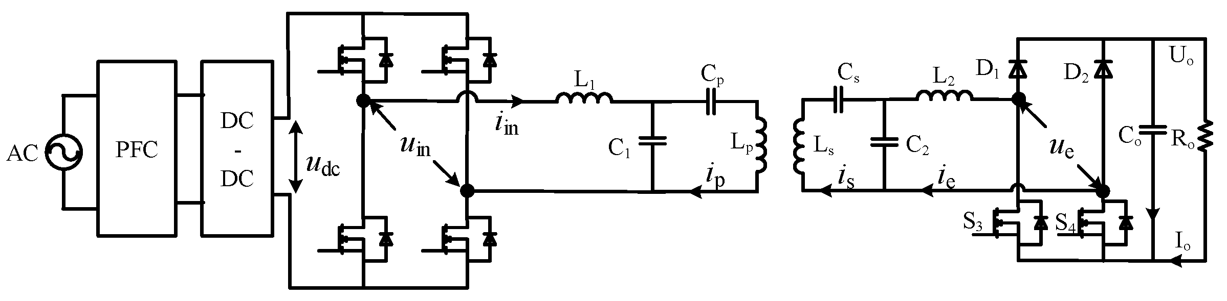
The present study used the previously described LCC-LCC resonant compensation network described [18]. This compensation topology is characterized by constant primary current, flexible parameter configuration, and optimal filtering effects. The characteristics hence make the LCC-LCC resonant compensation network suitable for use in the wireless charging system for EVs. An equivalent electrical circuit of the LCC-LCC EV-WPT system is presented in Figure 1.
The primary side of the electrical circuit of the LCC-LCC EV-WPT system shown in Figure 1 consists of an AC power source, tertiary structure power conversion modules, LCC compensation network, and transmitting coil. The power conversion modules include the PFC, DC-DC, and inverter. On the other side, the secondary side of the system consists of AC-induced current flows through the LCC compensation network, rectifier, and filtering capacitor, and then loads sequentially. In the secondary side, there are usually three full-bridge rectifier topologies; the basic one comprises the four diodes of the uncontrollable full-bridge circuit. These diodes have then been replaced by four switches with paralleled inverse diodes. Furthermore, only half the diodes are replaced by two switches with paralleled inverse diodes, which may be the best candidate to realize controllable regulation performance with relatively low cost and complexity. This study employed a fully controlled bridge rectifier, which is a novel control strategy that achieves full power output with high efficiency. The working principles of the secondary rectifier are illustrated in Figure 2.
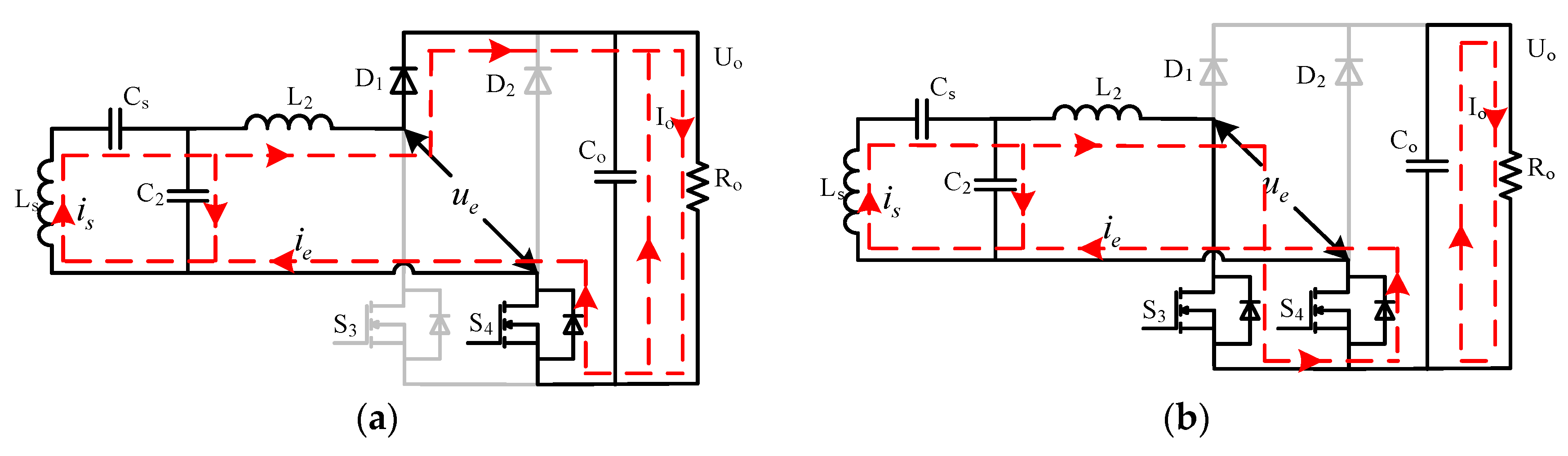
Rectification working status: The current ie flows through diode D1 and the power supply to the load, R0, then flows back to the LCC resonant compensation network. The output capacitor, C0, is charged in the process. Therefore, when the amplitude of voltage, ue, is equal to the output voltage V0, the RMS values of ue and ie can be calculated by:
Since the ue and ie phases are approximately equal, the equivalent impedance, Re, can be derived by:
Short-circuited working status: The current ie flows through S3 and S4, then returns to the compensation network when switches S3 and S4 are on. The load, R0, is powered by the discharging capacitor C0. In this circuit, when the amplitude of voltage, ue, is 0 and Re is 0. In this working setup, the EV-WPT system does not supply power to the load. However, when the direction of the current, ie, is reversed, the working principle is similar but was not further discussed in the current study. The power between the whole WPT system and the load is separate in this working status, which guarantees the safety of the load when emergencies occur. A control strategy can be developed by analyzing the two working statuses to realize the resonant compensation and optimization of output performance.
2.2. Control Principle and Analysis of the Rectifier Circuit
Control can be achieved through either the regulation of the duty cycle or phase shifting [19,20,21,22,23]. However, this study used the duty cycle regulation strategy. The different impedance characteristics of the equivalent impedance, Re, correspond to the ON moment of short-circuited working status during each working cycle, T. The three impedance properties analyzed in this study included capacitive impedance, inductive impedance, and resistive impedance.
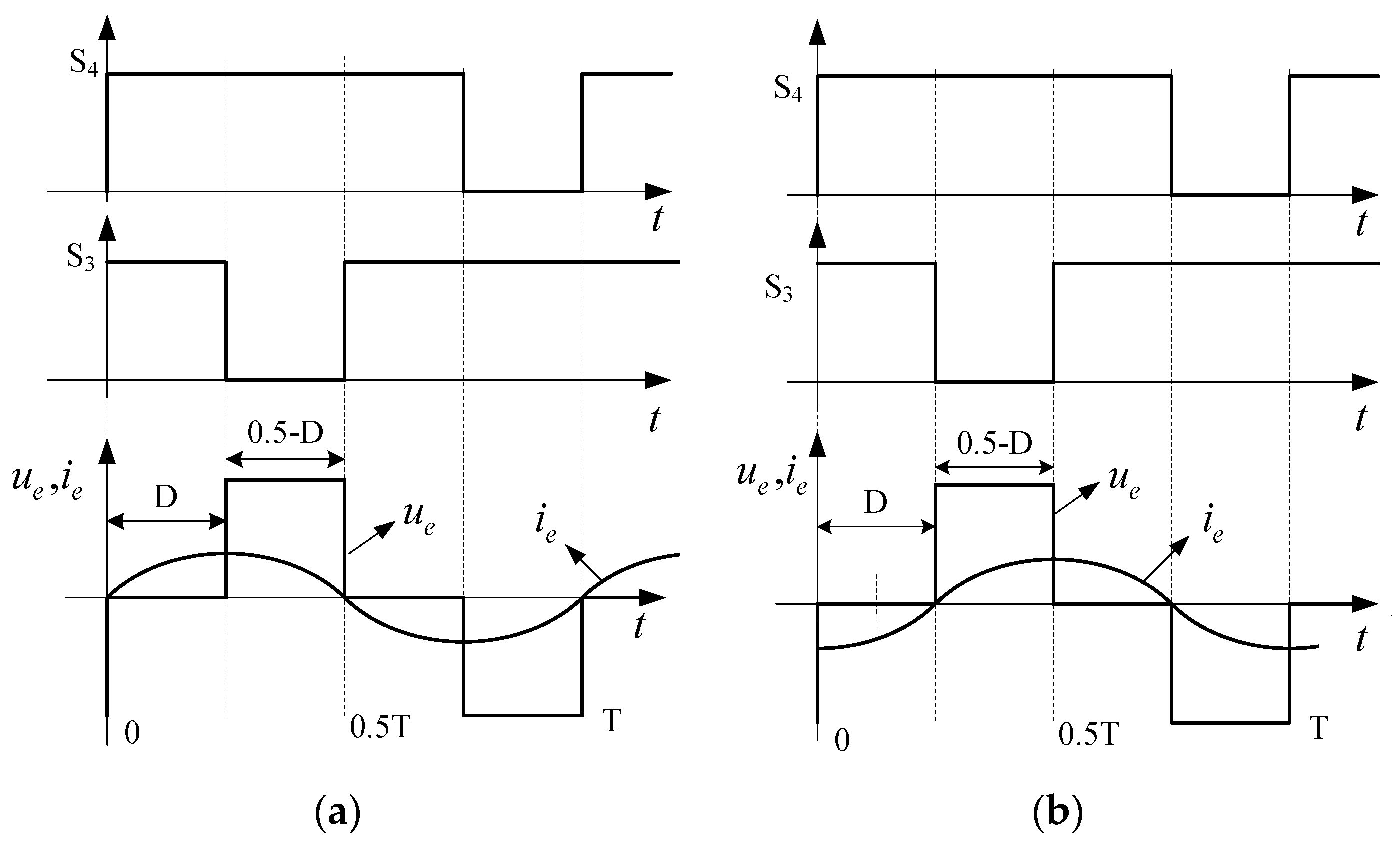
The driving signal of switches S3 and S4, as well as the waveforms of the current, ie, and voltage, ue, were as shown in Figure 3. The phase difference between the two switches was set to 180 degrees. Furthermore, for the positive half-period of ie, we let the working duration of the short-circuited working status to be T, and the working duration of the rectification’s working status to be (0.5-D) T.
According to the phase difference between ie and ue, it was concluded that switch S3 and S4 are ON at the zero point (positive or negative) of the ie waveform (Figure 3a). This means that the switches turn the zero current ON, not the zero current OFF; meanwhile, the zero voltage switch (ZVS) working conditions can also be employed. In Figure 3b, switches S3 and S4 are OFF at the zero point (positive or negative) of the ie waveform. The switches turn the zero current OFF, not the zero current ON, and the working conditions of the zero current switch (ZCS) can also be employed. In Figure 3c, the ON and OFF moment of switches S3 and S4 are controlled to realize the same phase between ie and ue, the imaginary part of Re is zero, and the hard switching is performed.
Only a fundamental harmonic is considered in our EV-WPT system. The current-voltage relationship for output voltage U0 and the RMS value of ue can be obtained by:
The current relationships of the output current, I0, and the RMS value of current ie, which flows through the rectifier, is constructed as:
If the current phase of ie is the reference phase, from (4) and (5), the output equivalent impedance of the secondary LCC resonant compensation network can be expressed as:
The real and imaginary part of Re, Re(Re), and Im(Re) can be further obtained:
where:
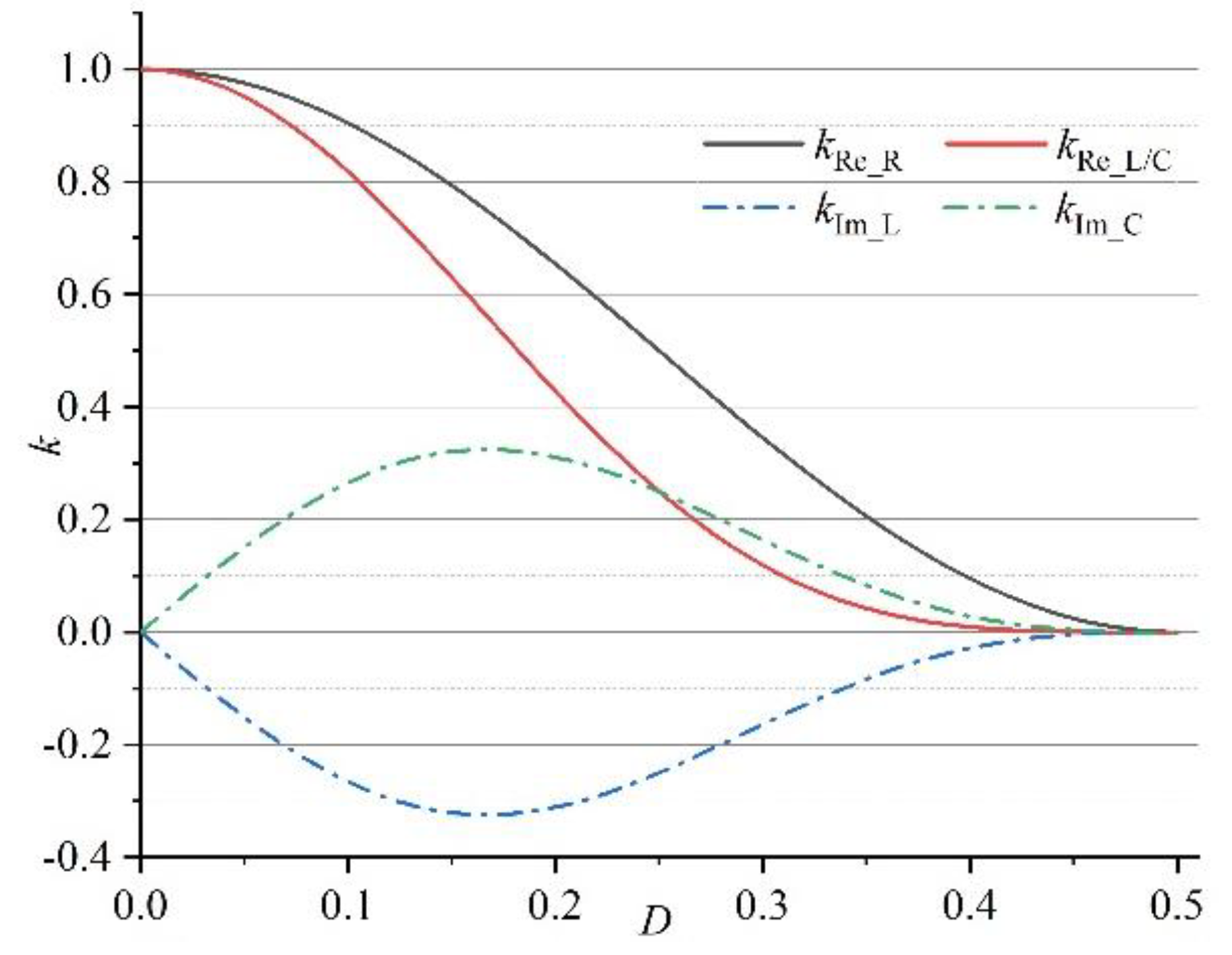
From the above formula, when our adopted circuit is under capacitive or inductive impedance compared with the uncontrollable rectifier circuit, the kIm coefficient is added to the imaginary part of Re, whereas the kRe_L/C coefficient is included in its real part. The kRe_L/C ranges from 0 to 1. When the imaginary coefficient value is negative, the capacitive impedance is achieved, and inductive impedance is achieved. Moreover, only the kRe coefficient is included in the Re when our adopted circuit is under resistive impedance as compared with the uncontrollable rectifier circuit. Furthermore, it is evident that the coefficient values of the real and imaginary parts are correlated with D as depicted in Figure 4.
Figure 4 shows that the coefficients of the real part under the three different impedance characteristics decrease with the increase in D. The dashed blue curve and dashed green curve represent the imaginary part of the inductive and capacitive impedance, and these absolute values initially increase and then decrease. The figure illustrates that the equivalent impedance can be modulated using the D values.
2.3. System Performance and Parameters Analysis
Figure 1 can further be modified into Figure 5, which illustrates the equivalent circuit model, based on the LCC-LCC resonant compensation network. Re, Z1, Z2, Z3, Z4, and Z5 are the equivalent impedances of each part. The Re(Re) and Im(Re) are defined in Equation (7) and can be optimized as controllable variables. For EV applications, when the gap or misalignment changes, the mutual inductance M, self-inductance Lp and Ls are variable terms. Furthermore, we define (1 + Γ)Lp and (1 + Λ)Ls as the self-inductance of transmitting and receiving the coil, respectively. The Γ and Λ represent the change in magnitude of self-inductance caused by variations in gap or tolerance.
When the system works on the resonant frequency ω0 in both primary and secondary sides, the following formula can be derived as:
The impedance and trans-conductance derivation of each part of the circuit (seen in Figure 5) are given as:
The current relationship in the LCC-LCC resonant compensation networks can also be derived:
From Equation (11), the input current Iin can be further derived as:
The power loss relationship is analyzed and the input voltage of the LCC–LCC resonant compensation network is assessed:
where φe is the phase angle of input current and voltage. When the power losses in other electronics are not taken into account, the input power can be expressed as:
When the internal resistance of L1 and L2 are not considered, the efficiency of the LCC-LCC resonant compensation network is derived as:
The list of typical parameters and variables used for the EV-WPT system is provided in Table 2.
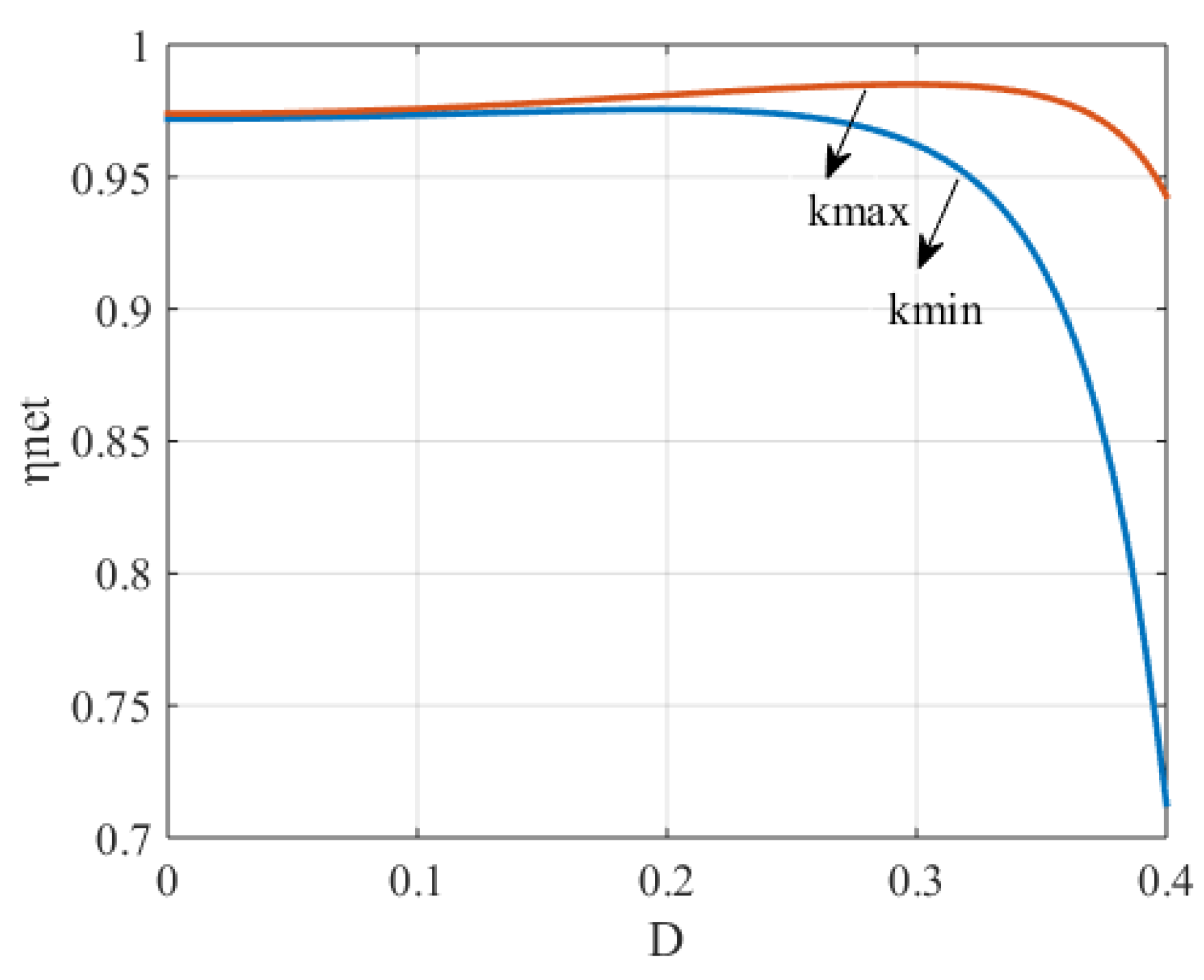
In Table 2, Lp and Ls are the transmitter and receiver coil self-inductances, and their specifications, including Lp, Ls, k and M, are referred to China’s global standard GB/T 38775-6 (electric vehicle wireless power transfer—Part 6: interoperability requirements and testing—ground side, and GB/T 38775-7 electric vehicle wireless power transfer—Part 7: interoperability requirements and testing - vehicle side [9]. The output parameters, such as Uout, include the range of output voltages at the rated output power, which is designed according to the required voltage of the battery. The inductors and capacitors in the LCC–LCC compensation network, such as L1, C1, L2, C2, Cp, and Cs, are derived by Equation (9). Iin-max is the maximum value of the inverter output current, while Iie-max is the maximum value of the rectifier output current. The value ranges (minimum and maximum) of Lp and Ls are set as Lp-kmax, Lp-kmin, Ls-kmax and Ls-kmin when the coupling coefficient k is set to kmax and kmin, respectively. Figure 6 represents the graph of an efficiency net vs. D, considering kmin and kmax, showing different correlations between the two parameters.
In Figure 6, the solid blue curve shows that the efficiency of an LCC–LCC resonant network initially increases with an increase in D, and then significantly decreases when k is set to kmin. The red line shows that the efficiency initially increases and then decreases when k is set to kmax. Figure 6 indicates that D should be designed, considering the larger efficiency values. Moreover, the correlation between efficiency and D shows a similar trend for the different k-values, characterized by an initial increase, followed by a decrease. The turning points of the variation curve are dependent on the k-values; there is a much larger increase in D in decreasing efficiency with the k-variation.
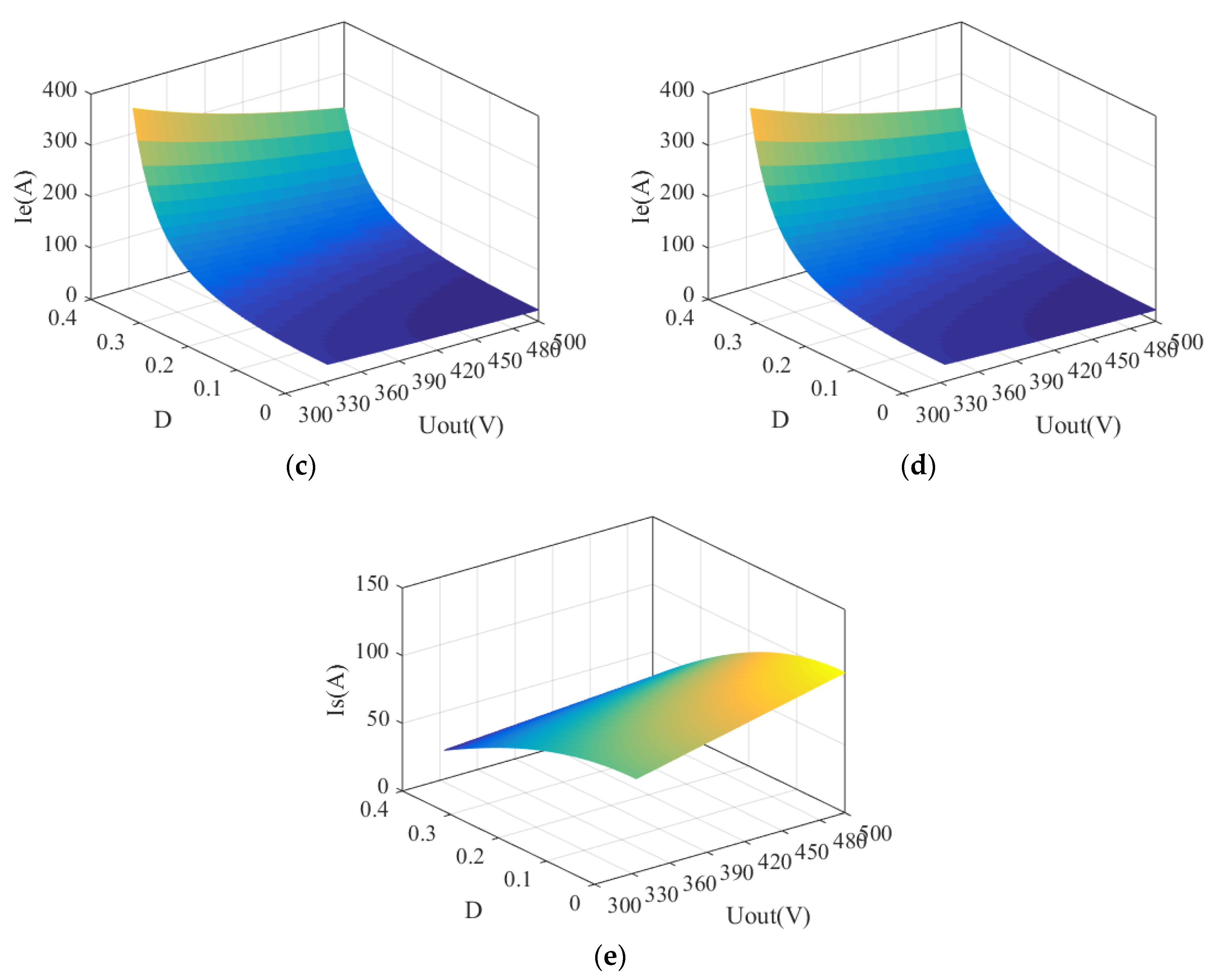
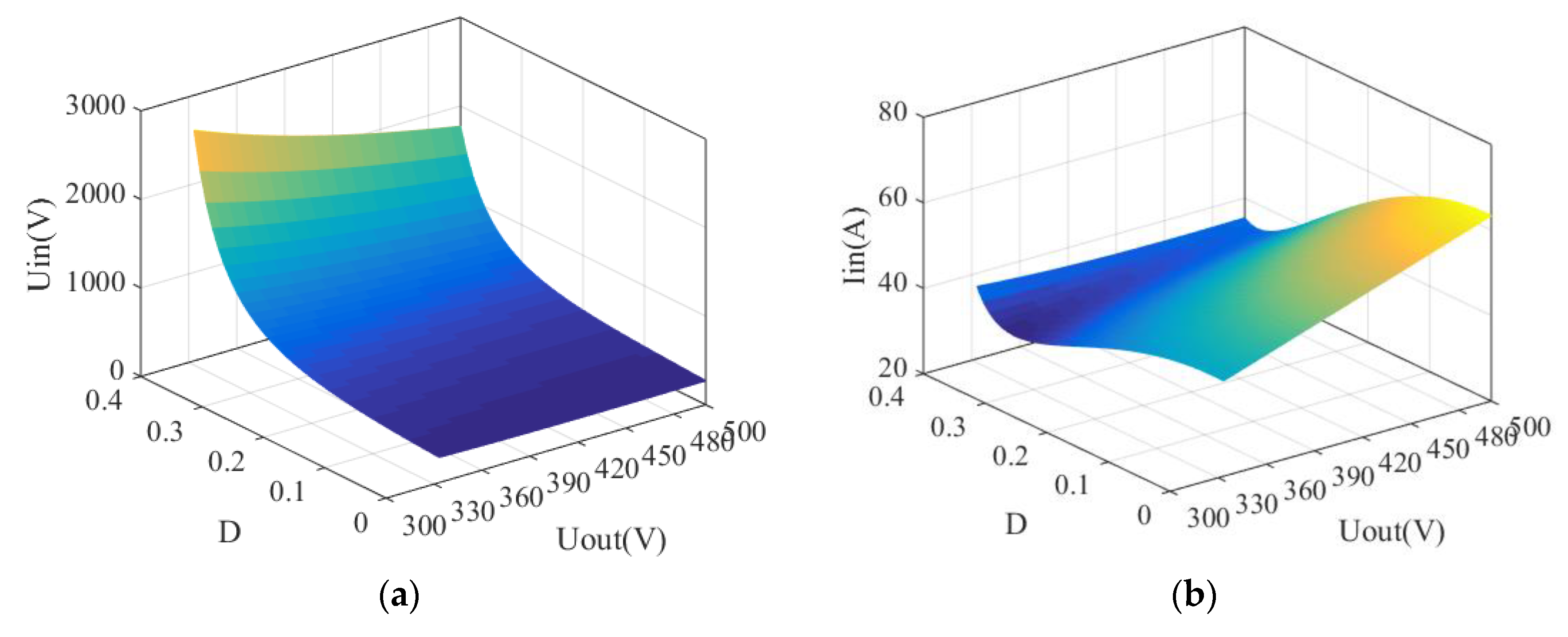
Moreover, variable D can directly affect the impedances in Figure 5, as well as the subsequent electric parameters and variables in the whole system. The changing trend of D can be compared with the secondary impedance characteristic, k. Figure 7 plots the variations in electric parameters and variables with different D and Uout under the capacitive impedance condition, with kmin, Uin, Iin, Ip, Ie, and Is. When the output power was set as 10 kW, the full power output was achieved, with an output voltage ranging between 320 and 450 V.
Figure 7 illustrates the finding that when the system parameters and variables, including D, are designed and the output power is set as 10 kW, the correlation between Uin and Iin is, therefore, opposite. Moreover, when the value of D exceeds a certain point, the efficiency rapidly declines, whereas Iin indicates an increasing trend.
Figure 8 plots graphs for when k was set as kmax, whereas the other parameters and variables remain as shown in Figure 7.
A comparison between Figure 7 and Figure 8 shows that when an arbitrary k-value is taken, Uin, Ip, and Ie increase with an increase in D, but decreases with the increase in Uout. Therefore, a large D value results in inappropriately large values of Uin, Ip, and Ie. Furthermore, it is evident that when an arbitrary k-value is taken, the Is decreases with an increase in D, but increases with an increase in Uout. This indicates that a very small value of D results in an inappropriately large Is value. When an arbitrary k-value is taken, an increase in D is associated with an initial decrease in Iin, followed by an increase. Therefore, D should be set in a way to avoid the under or oversizing of Iin. The changes in Ie with D show the opposite trend as Iin, which indicates the range of D is limited while existing electrical constraints. According to Equations (4)–(6), the secondary electric parameters and variables, Is and Ie, are mainly dependent on Uout and D and not be related to k. Therefore, according to the above description and analysis, it has been concluded that the primary electric parameters change with increasing k, but secondary variables are independent of k.
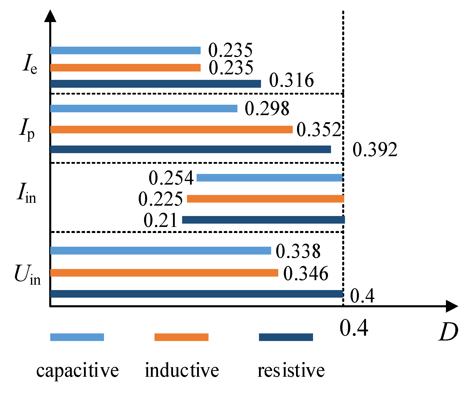
Therefore, the D value range should be optimized to ensure the full power output under capacitive impedance, as electronic constraints. The initial range of D = (0, 0.4) was used because of the unacceptable low efficiency with a larger D value. The range of D values is associated with the k-value. Table 3 displays the ranges of D values with different electronic constraints under capacitive impedance.
Similar analyses were done under inductive and resistive impedance. Details including three impedance working conditions are as shown in Figure 9.
In Figure 9, the range of D is mainly determined by Ie and Iin constraints. Under capacitive impedance, there is no D value set that can realize the full power output when k is kmax. The range of D is (0.225, 0.235) and (0.21, 0.236) when the system works under the inductive and resistive impedance, respectively.
Considering the heat dissipation, power loss, operational lifetime of the switching electronics, ZCS could not be achieved. Furthermore, the optimal working condition was zero current ON, then zero current OFF, and the worst was in hard-switching ON and OFF. Therefore, capacitive impedance was the best, whereas the resistive impedance was the worst among the three different impedance characteristics. In most charging scenarios, the capacitive impedance can meet all electrical constraints. A critical value of k is considered as k1, when the k-value is greater than k1, and there is no D solution. The range of D is larger under the inductive and resistive impedance condition, compared with the above condition. Therefore, a control strategy is proposed, based on the impedance characteristics.
3. Proposed Control Strategy
3.1. Range Constraints of System Parameter Values
The range of D narrows with an increase in k, as analyzed in the above section, and there is no D solution when k is set as kmax under capacitive impedance. This is attributed to the variations in Iin and Ie values. Moreover, the determination of k1 is the key variable in the whole strategy under the capacitive impedance model. However, k1 cannot be obtained in advance because EV charging applications are complex and inconsistent. In addition, the k1 value is impossible to obtain through online testing. Therefore, a characterization parameter was proposed in this study as follows:
The secondary impedance, as illustrated in Figure 5, can be expressed as:
When β is defined as the phase angle of the secondary impedance, and the phase angle of Ip is used as the reference, the open circuit voltage of the secondary side voc can be obtained as:
The current of the power-receiving coil is also derived as:
where Is is the RMS value of is. The apparent power of the secondary side can be derived as:
When the phase difference between ip and voc is 90 degrees, the value of ip and is are 90-β. Furthermore, according to Equation (19), the active power can be expressed as:
where Pout is the output power and ηVA is the efficiency of the secondary side, which can be approximately expressed as:
where PQS_loss is the power loss of the secondary rectifier, which can be expressed as:
where RDS (on), tf_s, and f are parameters for the switching electronics in the rectifier circuit denoting on-resistance, turn-off time, and working frequency, respectively. According to the above equations, the secondary impedance phase of β can be expressed as:
Then, the input current of the primary resonant compensation network can further be derived as:
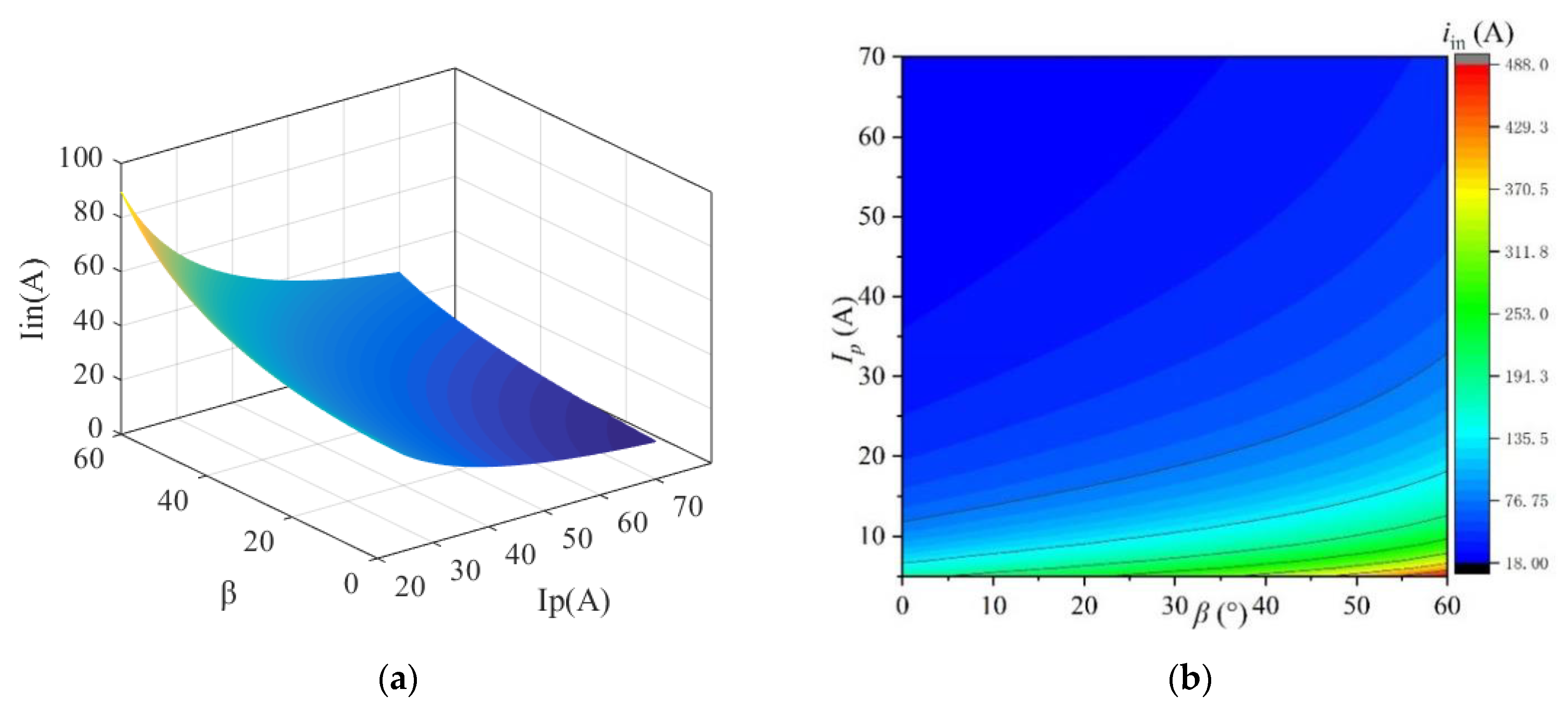
In Equation (24), Lp is the designed inductance of the primary transmitting coil, with a fixed working frequency. The Lp-kmin in Table 3 is the minimum value of Lp. Γ is the variation ratio of Lp with different k-values; the value of Γ in Table 3 is set as 0.0395. Pout is the desired output power and its value is 10 kW. Here, ω, L1, Lp and Γ are fixed values, whereas the ηVA varies only in a very small range that can be derived after parameter setting. Therefore, we can conclude that iin is relevant to Ip and β, whereas the iin constraint corresponds to β. When the values in Table 3 are adapted and the value of ηVA is set as 0.95, then the relationship between iin and Ip and β can be presented in Figure 10.
According to Figure 10, iin showed a positive correlation with β, and not with Ip. To meet the Iin constraints, the minimal limiting value of Ip and the maximum limiting values of β are required, which can be calculated using Equation (25). For Table 3, when the Iin values are less than 45 A, the limiting values of β with different Ip constraints are as listed in Table 4.
According to the results shown in Table 4, to meet the Iin constraints, the value of Ip should not be less than 20 A, and when Ip is equal to or greater than 42.6 A, all the β sets meet the Iin constraint demands. When the load resistance and other system parameters are determined, the Ip values can be derived by adjusting the input voltage value of the primary inverter. When Ip ≥ 20 A, measuring the β value can be used to judge whether the Iin value is beyond its constraints.
3.2. Proposed Control Method Based on Impedance Working Modes
According to Figure 9, the minimal limiting value of D is determined by Iin, while the maximum value is determined by Ie. When the value of Dmin is less than Dmax, the capacitive impedance working mode should be adopted. On the other hand, when Dmin ≥ Dmax, the inductive and resistive impedance working modes should be adopted. Dmax value can be derived using Equation (5); hence, the working mode is directly decided by Dmin. β should be detected and measured before the power transfer process.
β can be derived using Equation (24), and the M and ηVA values should be given. In the current study ηVA was set as 0.95, because ηVA should be greater than 0.9. Considering system performance, and an error range of <±5%, the calculated error range of β was around 1 degree. Therefore, before the wireless power transfer process, the value of β could be determined by measuring M.
Furthermore, the primary current Ip for the WPT system presented in Figure 1 can be expressed as:
where:
A1 and A2 are constant values, and M can be derived by detecting Ip and Ie when Re is set at 0. The constraint of resistance impedance working mode can be derived by M and Dmin. According to Table 4, the M constraints can be calculated when Ip is set to 20 A and β = 0. Based on Equation (24), M can be further expressed as:
To ensure that Iin is ≤45 A, Ip should be equal to or greater than 20 A. According to Equation (4), to meet the requirements of D and the full power output with Uout ≥ 320 V, the value of Ue should be equal to or greater than 288.2 V. Moreover, the M-limiting value is 14 μH when the efficiency of the secondary circuit is set as 100%.
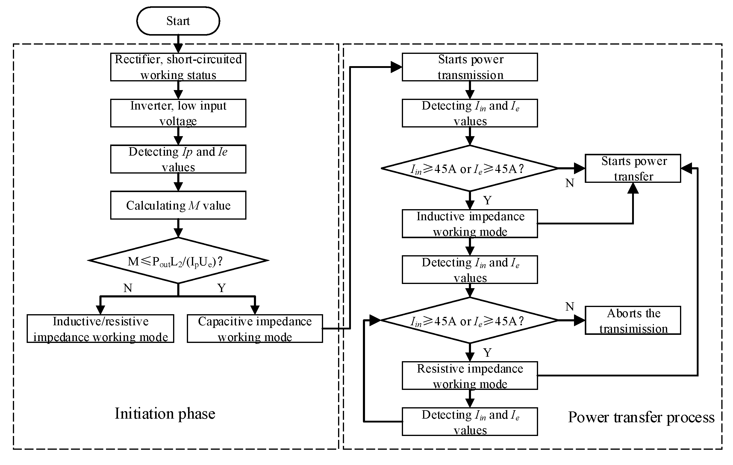
The flow diagram in the following Figure 11 illustrates the proposed control method workflow based on the impedance working modes.
The whole process is divided into two sub-processes—the initiation phase and the power transfer process. It was found that the secondary rectifier in the priming stage worked in the short-current conditions. Low voltage was provided to Ip ≤ 10 A, and M was derived by measuring Ip and Ie and using Equation (26). When M ≤ PoutL2/(IpUe), the capacitive working mode was chosen, and the second phase was carried out. Otherwise, when M > PoutL2/(IpUe), the inductive and resistive impedance working modes were chosen and the second phase was carried out. In the capacitive impedance power transfer process, the Iin and Ie values were measured, and the ranges were used to make decisions. When Iin ≥ 45 A or Ie ≥ 45 A, the working mode was switched to the inductive impedance, and if Iin < 45 A and Ie < 45 A, power transfer continued through the capacitive impedance charging mode. The described judgment conditions are then discussed again; if correct, they step into the resistive impedance working mode; otherwise, the charging process is aborted.
4. Experimental Validation
Figure 12 shows a photograph of an experimental system in which the circuit parameters and variables used in Table 3 were adopted.
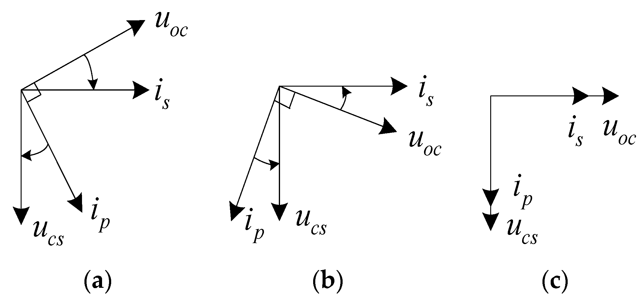
Zero-point tests in the ue and ie waveforms were performed to characterize the impedance working modes in the secondary side. However, the resistive impedance working mode cannot be judged by the described method. Furthermore, the primary current ip and voltage of the secondary capacitor Cs have the following relationships:
where uoc and is are the voltage and current of the secondary coil, respectively, the phase angle of ip lags by 90 degrees, corresponding to uoc, and the phase angle of the uCs lags by 90 degrees, corresponding to is. The corresponding phase relationships between the different impedance working modes are shown in Figure 13.
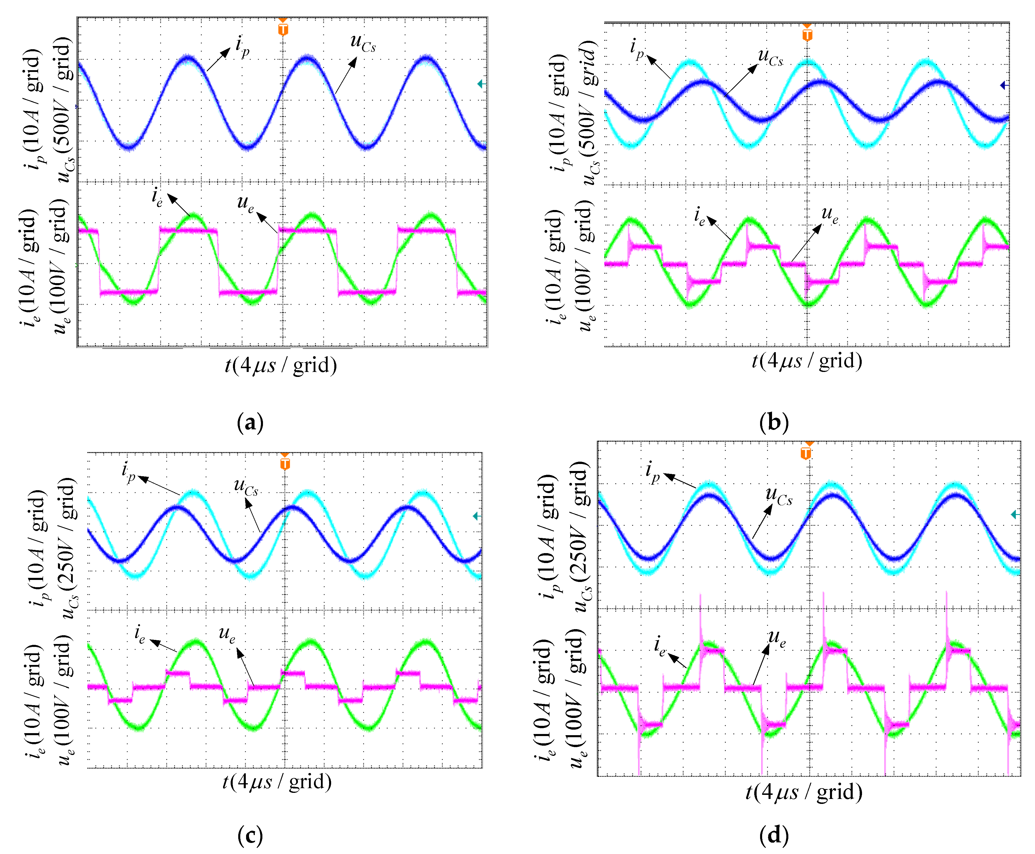
The current and voltage waveforms with an uncontrollable rectifier and three different impedance working modes are plotted as shown in Figure 14.
As shown in Figure 14a, when D was set to 0.5, the secondary side worked under uncontrollable conditions, the phase angle of ip and uCs were the same, the phase angle of ie and ue were the same, and the switching device realized zero-current ON and OFF. In Figure 14b, the secondary side worked under a capacitive working mode; the switching device enabled zero-current ON (the short-circuited mode works on the zero-crossing of ie), and ip was the phase leading with respect to uCs. In Figure 14c, the secondary side worked under an inductive working mode, the switching device realized the zero-current OFF (the short-circuited mode works before the zero-crossing of ie), and ip showed phase-lagging with respect to uCs. In Figure 14d, the secondary side worked under a resistive working mode, the switching device realized non-zero-current ON and non-zero-current OFF (short-circuited mode works between two zero-crossings of ie), and the phase was the same for ip and uCs. However, the peak voltage was relatively large when ON and OFF.
The above experimental results showed that our three proposed working modes can be achieved; the phase relationships and electrical characteristics obtained are in agreement with the theoretical analysis.
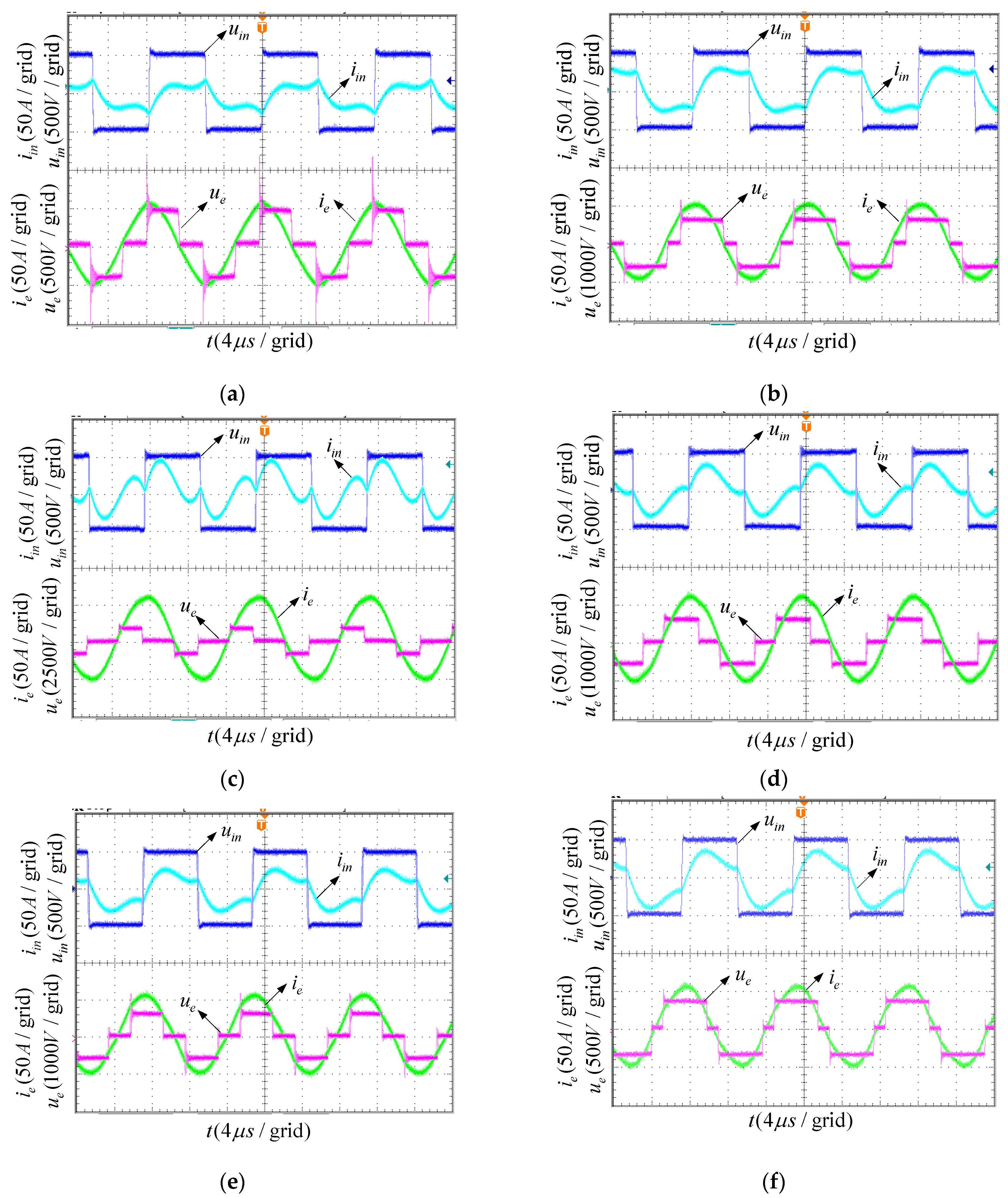
For the proposed experimental system, the upper maximum value of M was set at 14.53 μH (when the Tx and Rx coils are aligned and the transmitting gap is minimum), and the lower maximum value of M is at 5.163 μH (when the Tx and Rx coils are misaligned with a maximum tolerance and the transmitting gap is maximum) (Figure 12). The system output voltage was set at 450 V. Figure 15 illustrates the output waveforms and output power with different M values under three different working modes.
Figure 15b,d,f show that when M was set at Mnin, all three different working modes realized full-power output (10 kW). Figure 15c,e illustrate that when M was set at Mmax, the inductive and resistive impedance working modes realized full-power output. However, the output power only reached 8.5 kW under capacitive impedance working mode (Figure 15a). This is because the current Iin is limited, and there are no D working values to realize full-power output under a capacitive impedance working mode. On the contrary, the current Iin (Iin < 45 A) is not limited, and there are D working values to realize the full-power output under inductive and resistive impedance working modes.
The above experiments indicate that the M values can reasonably be set to choose the working mode. Meanwhile, this study has confirmed the correction of the proposed multi-modulation strategy.
5. Conclusions
The conclusions of our paper are as follows:
(1) The wide-ranging output performance can be optimized by controlling the duty cycle D of the rectifier on the secondary side under a fixed working frequency. The proposed multi-modulation scheme can be applied in the EVs’ wireless charging systems.
(2) The system performs different key electrical characteristics under different impedance working modes. The range values of D were different, and D was determined by Ie, Ip, Iin, and Uin constraints. The resistive working mode attained the maximum D range among three different impedance working modes, where the D range under the capacitive working mode achieved minimum values.
(3) The rectifier in the secondary side performs optimally under the capacitive impedance working mode and performs worst under the resistive impedance working mode. Therefore, the capacitive mode should be used as the initial working mode.
(4) Under the capacitive impedance working mode, there are no D values when the M value is at maximum, and the output voltage reaches the peak value. In this case, the working mode should be changed to achieve the full power output.
(5) A multi-modulation scheme was proposed, based on the M detection and phase angle of the secondary side, and the duty cycle of the rectifier D was the criterion used to control the impedance working mode.
Author Contributions
Conceptualization, W.L. and C.H.; methodology, W.L. and C.H.; software, L.X.; validation, W.L., C.H. and L.X.; formal analysis, L.X..; investigation, C.H.; resources, L.X.; data curation, W.L.; writing—original draft preparation, W.L. and C.H.; writing—review and editing, L.X.; visualization, W.L.; supervision, C.H.; project administration, C.H.; funding acquisition, L.X. All authors have read and agreed to the published version of the manuscript.
Funding
Shenzhen Science and Technology Program under grant WDZCJH20220814133504001, The National Natural Science Foundation of China under grant 62001301, the Project of Educational Commission of Guangdong Province of China under grant 2021KTSCX276, Post-doctoral Later-stage Foundation Project of Shenzhen Polytechnic under grant 6021271013K, Shenzhen Polytechnic Project under grant 6022310030K, the Key R&D Program of Guangdong Province, China under grant 2020B0404030004.
Conflicts of Interest
The authors declare no conflict of interest.
References
- Ruddell, S.; Madawala, U.K.; Thrimawithana, D.J. A Wireless EV Charging Topology with Integrated Energy Storage. IEEE Trans. Power Electron. 2020, 35, 8965–8972. [Google Scholar] [CrossRef]
- Liu, Y.; Madawala, U.K.; Mai, R.; He, Z. Zero-Phase-Angle Controlled Bidirectional Wireless EV Charging Systems for Large Coil Misalignments. IEEE Trans. Power Electron. 2020, 35, 5343–5353. [Google Scholar] [CrossRef]
- Luo, Z.; Wei, X.; Pearce, M.G.S.; Covic, G.A. Multiobjective Optimization of Inductive Power Transfer Double-D Pads for Electric Vehicles. IEEE Trans. Power Electron. 2020, 36, 5135–5146. [Google Scholar] [CrossRef]
- Mi, C.C.; Buja, G.; Choi, S.Y.; Rim, C.T. Modern Advances in Wireless Power Transfer Systems for Roadway Powered Electric Vehicles. IEEE Trans. Ind. Electron. 2016, 63, 6533–6545. [Google Scholar] [CrossRef]
- El-Shahat, A.; Ayisire, E. Novel Electrical Modeling, Design and Comparative Control Techniques for Wireless Electric Vehicle Battery Charging. Electronics 2021, 10, 2842. [Google Scholar] [CrossRef]
- IEC 61980-1:2020; Electric Vehicle Wireless Power Transfer (WPT) Systems—Part 1: General Requirements. IEC: Geneva, Switzerland, 2020. Available online: https://webstore.iec.ch/publication/31657 (accessed on 1 February 2022).
- ISO 19363:2020; Electrically Propelled Road Vehicles—Magnetic Field Wireless Power Transfer—Safety and Interoperability Requirements. ISO: Geneva, Switzerland, 2020. Available online: https://www.iso.org/standard/73547.html (accessed on 1 February 2022).
- Wireless Power Transfer for Light-Duty Plug-in/Electric Vehicles and Alignment Methodology J2954_202010. Available online: https://www.sae.org/standards/content/j2954_202010/ (accessed on 1 February 2022).
- Electric Vehicle Wireless Power Transfer—Part 1: General Requirements. Available online: http://std.samr.gov.cn/gb/search/gbDetailed?id=A47A713B75C414ABE05397BE0A0ABB25 (accessed on 1 February 2022).
- Li, W.; Zhao, H.; Deng, L.; Li, S.; Mi, C.C. Comparison Study on SS and Double-Sided LCC Compensation Topologies for EV/PHEV Wireless Chargers. IEEE Trans. Veh. Technol. 2016, 65, 4429–4439. [Google Scholar] [CrossRef]
- Kan, T.; Lu, F.; Nguyen, T.; Mercier, P.P.; Mi, C.C. Integrated Coil Design for EV Wireless Charging Systems Using LCC Compensation Topology. IEEE Trans. Power Electron. 2018, 33, 9231–9241. [Google Scholar] [CrossRef]
- Ali, N.; Liu, Z.; Hou, Y.; Armghan, H.; Wei, X.; Armghan, A. LCC-S Based Discrete Fast Terminal Sliding Mode Controller for Efficient Charging through Wireless Power Transfer. Energies 2020, 13, 1370. [Google Scholar] [CrossRef]
- Zakerian, A.; Vaez-Zadeh, S.; Babaki, A. A Dynamic WPT System with High Efficiency and High Power Factor for Electric Vehicles. IEEE Trans. Power Electron. 2020, 35, 6732–6740. [Google Scholar] [CrossRef]
- Kim, N.Y.; Kim, K.Y.; Choi, J.; Kim, C.W. Adaptive frequency with power-level tracking system for efficient magnetic resonance wireless power transfer. Electron. Lett. 2012, 48, 452–453. [Google Scholar] [CrossRef] [Green Version]
- Miller, J.M.; Onar, O.C.; Chinthavali, M. Primary-Side Power Flow Control of Wireless Power Transfer for Electric Vehicle Charging. IEEE J. Emerg. Sel. Top. Power Electron. 2015, 3, 147–162. [Google Scholar] [CrossRef]
- Tian, Y.; Zhu, Z.; Xiang, L.; Tian, J. Vision-Based Rapid Power Control for a Dynamic Wireless Power Transfer System of Electric Vehicles. IEEE Access 2020, 8, 78764–78778. [Google Scholar] [CrossRef]
- Gong, L.; Xiao, C.; Cao, B.; Zhou, Y. Adaptive Smart Control Method for Electric Vehicle Wireless Charging System. Energies 2018, 11, 2685. [Google Scholar] [CrossRef]
- Li, S.; Li, W.; Deng, J.; Nguyen, T.D.; Mi, C.C. A Double-Sided LCC Compensation Network and Its Tuning Method for Wireless Power Transfer. IEEE Trans. Veh. Technol. 2015, 64, 2261–2273. [Google Scholar] [CrossRef]
- Jiang, Y.; Wang, L.; Fang, J.; Li, R.; Han, R.; Wang, Y. A High-Efficiency ZVS Wireless Power Transfer System for Electric Vehicle Charging with Variable Angle Phase Shift Control. IEEE J. Emerg. Sel. Top. Power Electron. 2020, 9, 2356–2372. [Google Scholar] [CrossRef]
- Wu, J.; Bie, L.; Kong, W.; Gao, P.; Wang, Y. Multi-Frequency Multi-Amplitude Superposition Modulation Method With Phase Shift Optimization for Single Inverter of Wireless Power Transfer System. IEEE Trans. Circuits Syst. I Regul. Pap. 2021, 68, 2271–2279. [Google Scholar] [CrossRef]
- Xia, C.; Jia, R.; Shi, Y.; Hu, A.P.; Zhou, Y. Simultaneous Wireless Power and Information Transfer Based on Phase-Shift Modulation in ICPT System. IEEE Trans. Energy Convers. 2020, 36, 629–639. [Google Scholar] [CrossRef]
- Yao, Y.; Gao, S.; Wang, Y.; Liu, X.; Zhang, X.; Xu, D. Design and Optimization of an Electric Vehicle Wireless Charging System Using Interleaved Boost Converter and Flat Solenoid Coupler. IEEE Trans. Power Electron. 2020, 36, 3894–3908. [Google Scholar] [CrossRef]
- Kim, M.J.; Woo, J.W.; Kim, E.S. Single stage AC-DC converter for wireless power transfer operating within wide voltage control range. J. Power Electron. 2021, 21, 768–781. [Google Scholar] [CrossRef]
Figure 1.
Electrical configuration for LCC-LCC EV-WPT system.

Figure 2.
Schematic illustration of the rectifier’s working principle: (a) rectification working status; (b) short-circuited working status.
Figure 2.
Schematic illustration of the rectifier’s working principle: (a) rectification working status; (b) short-circuited working status.

Figure 3.
Impedance categories using duty cycle regulation: (a) capacitive impedance; (b) inductive impedance; (c) resistive impedance.
Figure 3.
Impedance categories using duty cycle regulation: (a) capacitive impedance; (b) inductive impedance; (c) resistive impedance.


Figure 4.
The relationship between the coefficients and D.

Figure 5.
Equivalent circuit of the LCC-LCC EV-WPT system.

Figure 6.
Efficiency variations vs. D with kmin and kmax.

Figure 7.
Electric parameter variations with different D and Uout values under capacitive impedance conditions, with kmin: (a) Uin variation values; (b) Iin variation values; (c) Ip variation values; (d) Ie variation values; (e) Is variation values.
Figure 7.
Electric parameter variations with different D and Uout values under capacitive impedance conditions, with kmin: (a) Uin variation values; (b) Iin variation values; (c) Ip variation values; (d) Ie variation values; (e) Is variation values.


Figure 8.
Electric parameter variations with different D and Uout under capacitive impedance condition with kmax: (a) Uin variation values; (b) Iin variation values; (c) Ip variation values; (d) Ie variation values; (e) Is variation values.
Figure 8.
Electric parameter variations with different D and Uout under capacitive impedance condition with kmax: (a) Uin variation values; (b) Iin variation values; (c) Ip variation values; (d) Ie variation values; (e) Is variation values.


Figure 9.
Ranges of D under different constraints.

Figure 10.
Relationship between iin and Ip, β: (a) curve plot (b) contour plot.

Figure 11.
Flowchart of proposed control method.

Figure 12.
Experimental setup.

Figure 13.
Phase angles with different impedance working modes: (a) Capacitive impedance working mode (b) inductive impedance working mode (c) resistive impedance working mode.
Figure 13.
Phase angles with different impedance working modes: (a) Capacitive impedance working mode (b) inductive impedance working mode (c) resistive impedance working mode.

Figure 14.
Experimental waveforms with different working modes: (a) uncontrollable rectifier; (b) capacitive impedance working mode; (c) inductive impedance working mode; (d) resistive impedance working mode.
Figure 14.
Experimental waveforms with different working modes: (a) uncontrollable rectifier; (b) capacitive impedance working mode; (c) inductive impedance working mode; (d) resistive impedance working mode.

Figure 15.
Experimental waveforms with different working modes and different M values: (a) capacitive impedance working mode with Mmax; (b) capacitive impedance working mode with Mmin; (c) inductive impedance working mode with Mmax; (d) inductive impedance working mode with Mmin; (e) resistive impedance working mode with Mmax; (f) resistive impedance working mode with Mmin.


Table 1.
Charging classifications for EV wireless charging.
| Requirements | Classifications | Values |
|---|---|---|
| Gap | Z1 | 100–150 (mm) |
| Gap | Z2 | 140–210 (mm) |
| Gap | Z3 | 170–250 (mm) |
| Input power level | WPT1 | 3.7 (kW) |
| Input power level | WPT2 | 7.7 (kW) |
| Input power level | WPT3 | 11.1 (kW) |
| Tolerance | X-axis (EV moving direction) | ±75 (mm) |
| Tolerance | Y-axis (vertical direction of X-axis) | ±100 (mm) |
| System efficiency | Aligned | ≥85% |
| System efficiency | Misalignment | ≥80% |
Table 2.
EV-WPT system parameters and variables.
| Parameters | Values | Parameters | Values | Parameters | Values | Parameters | Values |
|---|---|---|---|---|---|---|---|
| L1 (μH) | 22 | Cs (nH) | 60.349 | Ls-kmin (μH) | 65.517 | kmin | 0.093 |
| L2 (μH) | 8.1 | Uout (V) | 300–450 | Mmax (μH) | 14.53 | Iin-max (A) | 45 |
| C1 (nH) | 157.5 | Lp-kmax (μH) | 46.795 | Mmin (μH) | 5.163 | Ie-max (A) | 45 |
| C2 (nH) | 427.783 | Lp-kmin (μH) | 45.018 | Udc (V) | 100 | F (kHz) | 85.5 |
| Cp (nH) | 136 | Ls-kmax (μH) | 67.79 | kmax | 0.263 | R0 (Ω) | 10.0 |
Table 3.
Different D ranges with different electrical constraints.
| Parameters | Maximum Values | k Set | D Value Range |
|---|---|---|---|
| Uin (V) | 1200 | kmin | 0–0.21 |
| Uin (V) | 1200 | kmax | 0–0.338 |
| Iin (A) | 45 | kmin | 0–0.4 |
| Iin (A) | 45 | kmax | 0.254–0.4 |
| Ip (A) | 70 | kmin | 0–0.132 |
| Ip (A) | 70 | kmax | 0–0.298 |
| Is (A) | 100 | arbitrary values | 0–0.4 |
| Is (A) | 1200 | arbitrary values | 0–0.235 |
Table 4.
EV-WPT system parameters.
| Parameters | Constraint Values | ||||
|---|---|---|---|---|---|
| Ip | 10 | 20 | 30 | 40 | 42.6 |
| β | NaN | 0 | ≤46.5 | ≤58 | ≤90 |
Publisher’s Note: MDPI stays neutral with regard to jurisdictional claims in published maps and institutional affiliations. |
© 2022 by the authors. Licensee MDPI, Basel, Switzerland. This article is an open access article distributed under the terms and conditions of the Creative Commons Attribution (CC BY) license (https://creativecommons.org/licenses/by/4.0/).
Share and Cite
MDPI and ACS Style
Liu, W.; Hu, C.; Xiang, L. A Multimodal Modulation Scheme for Electric Vehicles’ Wireless Power Transfer Systems, Based on Secondary Impedance. Electronics 2022, 11, 3055. https://doi.org/10.3390/electronics11193055
AMA Style
Liu W, Hu C, Xiang L. A Multimodal Modulation Scheme for Electric Vehicles’ Wireless Power Transfer Systems, Based on Secondary Impedance. Electronics. 2022; 11(19):3055. https://doi.org/10.3390/electronics11193055
Chicago/Turabian StyleLiu, Wei, Chao Hu, and Lijuan Xiang. 2022. "A Multimodal Modulation Scheme for Electric Vehicles’ Wireless Power Transfer Systems, Based on Secondary Impedance" Electronics 11, no. 19: 3055. https://doi.org/10.3390/electronics11193055
Note that from the first issue of 2016, this journal uses article numbers instead of page numbers. See further details here.