Abstract
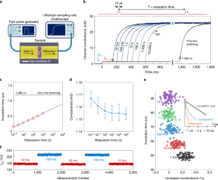
Metal–oxide–semiconductor junctions are the building blocks of modern electronics and can provide a variety of functionalities, from memory to computing. The technology, however, faces constraints in terms of further miniaturization and compatibility with post–von Neumann computing architectures. Manipulation of structural—rather than electronic—states could provide a path to ultrascaled low-power functional devices, but the electrical control of such states is challenging. Here we report electronically accessible long-lived structural states in vanadium dioxide that can provide a scheme for data storage and processing. The states can be arbitrarily manipulated on short timescales and tracked beyond 10,000 s after excitation, exhibiting features similar to glasses. In two-terminal devices with channel lengths down to 50 nm, sub-nanosecond electrical excitation can occur with an energy consumption as small as 100 fJ. These glass-like functional devices could outperform conventional metal–oxide–semiconductor electronics in terms of speed, energy consumption and miniaturization, as well as provide a route to neuromorphic computation and multilevel memories.
This is a preview of subscription content, access via your institution
Access options
Access Nature and 54 other Nature Portfolio journals
Get Nature+, our best-value online-access subscription
$29.99 / 30 days
cancel any time
Subscribe to this journal
Receive 12 digital issues and online access to articles
$119.00 per year
only $9.92 per issue
Buy this article
- Purchase on Springer Link
- Instant access to full article PDF
Prices may be subject to local taxes which are calculated during checkout


Data availability
All the data supporting the claims of this paper are available from the corresponding authors upon reasonable request.
References
Dagotto, E. Complexity in strongly correlated electronic systems. Science 309, 257–262 (2005).
Shao, Z. W., Cao, X., Luo, H. & Jin, J. P. Recent progress in the phase-transition mechanism and modulation of vanadium dioxide materials. NPG Asia Mater. 10, 581–605 (2018).
Oh, S. et al. Energy-efficient Mott activation neuron for full-hardware implementation of neural networks. Nat. Nanotechnol. 16, 680–687 (2021).
Bohaichuk, S. M. et al. Fast spiking of a Mott VO2-carbon nanotube composite device. Nano Lett. 19, 6751–6755 (2019).
Briggs, R. M., Pryce, I. M. & Atwater, H. A. Compact silicon photonic waveguide modulator based on the vanadium dioxide metal-insulator phase transition. Opt. Express 18, 11192–11201 (2010).
Strelcov, E., Lilach, Y. & Kolmakov, A. Gas sensor based on metal–insulator transition in VO2 nanowire thermistor. Nano Lett. 9, 2322–2326 (2009).
Eyert, V. The metal-insulator transitions of VO2: a band theoretical approach. Ann. Phys. 514, 650–702 (2002).
del Valle, J. et al. Spatiotemporal characterization of the field-induced insulator-to-metal transition. Science 373, 907–911 (2021).
Nakano, M. et al. Collective bulk carrier delocalization driven by electrostatic surface charge accumulation. Nature 487, 459–462 (2012).
Shukla, N. et al. A steep-slope transistor based on abrupt electronic phase transition. Nat. Commun. 6, 7812 (2015).
Liu, M. et al. Terahertz-field-induced insulator-to-metal transition in vanadium dioxide metamaterial. Nature 487, 345–348 (2012).
Gao, X., Rosário, C. M. M. & Hilgenkamp, H. Multi-level operation in VO2-based resistive switching devices. AIP Adv. 12, 015218 (2022).
del Valle, J. et al. Subthreshold firing in Mott nanodevices. Nature 569, 388–392 (2019).
Fisher, B., Patlagan, L. & Reisner, G. M. Sliding twin-domains in self-heated needle-like VO2 single crystals. Sci. Rep. 10, 6833 (2020).
del Valle, J. et al. Generation of tunable stochastic sequences using the insulator–metal transition. Nano Lett. 22, 1251–1256 (2022).
Samizadeh Nikoo, M. et al. Nanoplasma-enabled picosecond switches for ultrafast electronics. Nature 579, 534–539 (2020).
Shabalin, A. G. et al. Nanoscale imaging and control of volatile and non-volatile resistive switching in VO2. Small 16, 2005439 (2020).
Strukov, D. B., Snider, G. S., Stewart, D. R. & Williams, R. S. The missing memristor found. Nature 453, 80–83 (2008).
Wei, J., Wang, Z., Chen, W. & Cobden, D. H. New aspects of the metal–insulator transition in single-domain vanadium dioxide nanobeams. Nat. Nanotechnol. 4, 420–424 (2009).
Ramírez, J. G., Sharoni, A., Dubi, Y., Gómez, M. E. & Schuller, I. K. First-order reversal curve measurements of the metal-insulator transition in VO2: signatures of persistent metallic domains. Phys. Rev. B 79, 235110 (2009).
Abreu, E. et al. Nucleation and growth bottleneck in the conductivity recovery dynamics of nickelate ultrathin films. Nano Lett. 20, 7422 (2020).
Cheng, S. et al. Inherent stochasticity during insulator–metal transition in VO2. Proc. Natl Acad. Sci. USA 118, e2105895118 (2021).
Sohn, A., Kanki, T., Sakai, K., Tanaka, H. & Kim, D.-W. Fractal nature of metallic and insulating domain configurations in a VO2 thin film revealed by Kelvin probe force microscopy. Sci. Rep. 5, 10417 (2015).
Vaskivskyi, I. et al. Controlling the metal to insulator relaxation of the metastable hidden quantum state in 1T-TaS2. Sci. Adv. 1, e1500168 (2015).
Lee, S. et al. Electronic structure and insulating gap in epitaxial VO2 polymorphs. Appl. Mater. 3, 126109 (2015).
He, Z. & Millis, A. J. Photoinduced phase transitions in narrow-gap Mott insulators: the case of VO2. Phys. Rev. B 93, 115126 (2016).
Palmer, R. G., Stein, D. L., Abrahams, E. & Anderson, P. W. Models of hierarchically constrained dynamics for glassy relaxation. Phys. Rev. Lett. 53, 958–961 (1984).
Heckshera, T. et al. Toward broadband mechanical spectroscopy. Proc. Natl Acad. Sci. USA 114, 8710–8715 (2017).
Qazilbash, M. M. et al. Mott transition in VO2 revealed by infrared spectroscopy and nano-imaging. Science 318, 1750–1753 (2007).
Claassen, J. H., Lu, J. W., West, K. G. & Wolf, S. A. Relaxation dynamics of the metal-semiconductor transition in VO2 thin films. Appl. Phys. Lett. 96, 132102 (2010).
Prezioso, M. et al. Training and operation of an integrated neuromorphic network based on metal-oxide memristors. Nature 521, 61–64 (2015).
Ionescu, A. M. & Riel, H. Tunnel field-effect transistors as energy-efficient electronic switches. Nature 479, 329–337 (2011).
Pi, S. et al. Memristor crossbar arrays with 6-nm half-pitch and 2-nm critical dimension. Nat. Nanotechnol. 14, 35–39 (2019).
Wang, P. F. et al. A semi-floating gate transistor for low-voltage ultrafast memory and sensing operation. Science 341, 640–643 (2013).
Manca, N. et al. Selective high-frequency mechanical actuation driven by the VO2 electronic instability. Adv. Mater. 29, 1701618 (2017).
Hollander, M. J. et al. Electrically driven reversible insulator–metal phase transition in 1T-TaS2. Nano Lett. 15, 1861–1866 (2015).
Grimaldi, E. et al. Single-shot dynamics of spin–orbit torque and spin–transfer torque switching in three-terminal magnetic tunnel junctions. Nat. Nanotechnol. 15, 111–117 (2020).
Yang, J. J., Strukov, D. B. & Stewart, D. R. Memristive devices for computing. Nat. Nanotechnol. 8, 13–24 (2013).
Acknowledgements
We are grateful to the help of the staff at the Center of Micro and Nano Technology (CMi) at EPFL with the fabrication process. We thank A. Ionescu for discussions. Y.P. and J.S. acknowledge support for the PLD growth from the Basic Science Research Program (2020R1A4A1018935) through the National Research Foundation of Korea (NRF) funded by the Ministry of Science and ICT.
Author information
Authors and Affiliations
Contributions
M.S.N. and E.M. conceived the project. M.S.N., E.M. and P.J.W.M. proposed the mechanism hypothesis. A. Krammer, Y.P., A.S. and J.S. synthesized the VO2 films. M.S.N. fabricated the devices and performed and analysed the electrical measurements. R.S. performed and analysed the thermal microscopy measurements. G.M.M. and A. Kis performed and analysed the Kelvin probe force microscopy measurements. M.S.N. and E.M. wrote the manuscript with input from all the authors.
Corresponding authors
Ethics declarations
Competing interests
The authors declare no competing interests.
Peer review
Peer review information
Nature Electronics thanks the anonymous reviewers for their contribution to the peer review of this work.
Additional information
Publisher’s note Springer Nature remains neutral with regard to jurisdictional claims in published maps and institutional affiliations.
Extended data
Extended Data Fig. 1 Investigation on the possible effect of temperature rise on the observed memory effect.
a, Measured current of a VO2 switch under triangular excitation. The MIT happens between points A and B with a short time separation of ΔtAB ≈ 100 ns. The inset presents the extracted resistance of the device in the IMT and MIT cycles showing that post excitation resistance is close (within 1%) to the pre-IMT resistance. This is another indication of the fast sub-microsecond cooling. b, Thermal microscopy of a two-terminal VO2 switch triggered by 10-μs pulses (Vset = 2.1 V) with three different frequencies 0.1 Hz, 1 Hz and 10 Hz. The captured average temperature over the device does not show any notable difference between the three cases. This indicates that given the long time duration of our observed memory, this memory effect cannot be originated from thermal effects. c,d, Investigation of the memory effect for different excitation amplitudes Vset = 4.2 V and 2.1 V, respectively. If thermal effects induced the memory effect, then the 4.2 V excitation should result in a more pronounced change in the incubation time, because it leads to a higher temperature rise comparing to 2.1 V excitation. The measured incubation times, however, are identical, which disproves the role of thermal effects in our observed memory.
Extended Data Fig. 2 Evaluation of Vanadium Dioxide film and fabricated devices.
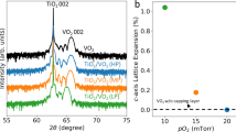
a, The θ − 2θ X-ray diffraction (XRD) pattern, recorded in the 20° – 75° (2𝜃) range. The result indicates that the sample is crystallized in the single monoclinic phase as all diffraction peaks are indexed to monoclinic VO2 (M1) crystal structure according to PDF 04-003-4401 (Space group P21/c, a = 5.75 Å, b = 4.52 Å, c = 5.38 Å, β = 122.6°). b, Resistance versus temperature of a two-port VO2 switch. c, Threshold consistency indicating no degradation in a 3-μm-long VO2 switch. d,e, Reproducibility of the results in devices with other metallic pads. Two-port switches fabricated on the high resistivity silicon substrate, based on VO2 / Ti (10 nm) / Pt (200 nm) and VO2 / Pt (200 nm) structures, exhibit identical memory behavior. f, Measured incubation times over 100 consecutive measurements for three devices with identical geometries with 500-nm-long channels. g, Consistency of the memory effect defined as \(m = t_{{{{\mathrm{inc}}}}}^{{{{\mathrm{ref}}}}}/t_{{{{\mathrm{inc}}}}} - 1\) for ten devices with the same geometry. \(t_{{{{\mathrm{inc}}}}}^{{{{\mathrm{ref}}}}}\) is the incubation of the reference pulse (corresponding to 1 second relaxation), and tinc represents the incubation time corresponding to pulses with 10 ms (blue columns) or 100 ms (orange columns) relaxation times.
Extended Data Fig. 3 Reproducibility of the results on a single-crystal VO2 samples on TiO2 and Al2O3 substrates.
Symmetrical 2θ-θ XRD scan on the a, 10 nm-thick VO2 film grown on (001) TiO2 substrate (VO2-on-TiO2), and b, 100 nm thick VO2 film grown on (0001) Al2O3 (VO2-on-Al2O3). c, Sheet resistance measurements on VO2-on-TiO2 and VO2-on-Al2O3 samples in the heating cycle. In case of VO2 grown on the (001) TiO2 substrate, which is strained along the c-axis by -1.2%, the transition temperature is shifted from ~340 K to ~292 K. d,e, Pulsed-measurements with two relaxation times - 1-ms and 1-s - on VO2-on-TiO2 and VO2-on-Al2O3 samples, showing the strong dependence of tinc on the relaxation time. In case of the VO2-on-TiO2 sample, the stage temperature was 5 °C to ensure that the film reverts back to the insulating state after removing the excitation.
Extended Data Fig. 4 Effect of inter-packet pulse separation on manipulation of the device state.
a, Schematic of a waveform corresponding to a single-pulse excitation (Vset = 2.7 V and 1-μs pulse width) and sensing incubation time after the relaxation time T = 1 s. b, Schematic of waveform corresponding to N-pulse excitation (identical pulses to part a) with inter-packet pulse separation ΔT and sensing the incubation time after the relaxation time T = 1 s. c, Measured incubation time on a 500-nm-long channel device for single pulse excitation and multiple pulse excitation (N = 10) with ΔT = 10 ms, 1 ms, 100 μs, 10 μs. The results clearly shows the state manipulation capability with multiple pulse excitation; however, the inter-packet pulse separation plays no role in the state manipulation.
Extended Data Fig. 5 Thermal activation of IMT using isolated heaters.
a, Optical micrograph of a VO2 switch integrated with two electrically isolated heaters. The scale bar corresponds to 10 μm. b, Captured thermal micrograph of the device with the heaters are triggered at their threshold voltage (18 V). The scale bar corresponds to 10 μm. c, Measured temperature over the cutline shown in part B indicating that the temperature at the middle switch (gap) considerably surpasses the IMT temperature. The measurement is done at the steady state; however, considering a sub-microsecond thermal time constant (Extended Data Fig. 1), for a 20-μs long excitation on the heaters, a thermal IMT in the middle switch is expected.
Extended Data Fig. 6 In-situ kelvin probe force microscopy to observe possible long-lived metallic domains.
a, Illustration of the KPFM experimental setup with in-situ electrical excitation to monitor possible long-lived metallic domains after electrically-driven IMT. If some metallic domains can possibly survive at room temperature and are responsible for the hours-long memory, one expects to capture a nonuniform surface potential map38. b, Gradient of the KPFM signal corresponding to the post-IMT scanning indicates visually no difference between the VO2 layer and the metallic pads (serving as reference), which is not supportive for long-lived metallic domains at the resolution of the KPFM scan (~30 nm) to be responsible for the observed memory.
Extended Data Fig. 7 Investigation on the effect of VO2 channel length on the observed memory.
VO2 switches with different channel lengths ranging from 500 nm down to 50 nm and fixed width of 20 µm were investigated. The memory effect was probed by applying double pulses with relaxation times of 10 ms and 1 s. The measured VO2 current for a, 500-nm-long channel VO2 switch (Vset = 2.8 V). b, 200-nm-long channel VO2 switch (Vset = 1.65 V). c, 100-nm-long channel VO2 switch (Vset = 1.25 V). d, 50-nm-long channel VO2 switch (Vset = 0.95 V). The voltage of each device was set to result in almost identical incubation times in the first reference pulse (blue curves). Despite the considerable difference in the VO2 channel lengths, the second pulses exhibited similar incubation times. These results show that the memory effect is identical among devices and not a strong function of channel length. This suggests that the observed phenomena are not attributed to any mesoscopic length scale.
Extended Data Fig. 8 Evaluation of threshold voltage, resistance and the incubation time of a VO2 switch.
a, IMT threshold voltage and resistance of a 1-µm-long channel VO2 switch measured at different relaxation times. Both parameters show similar trends, although the change in the threshold voltage is ten times larger than that of the resistance. Both parameters stabilize at in a few seconds and do not show logarithmic relaxation. We note that the MIT threshold voltage was totally independent from the relaxation time. b, Measured incubation revealed the information of previous switching events when the threshold and resistance are constant. Each data point corresponds to at least 20 measurements (error bars defined) with the exception of the T = 1000 s where we collected three data points. The results show that the memory effect embedded in the incubation time is independent from the changes in the threshold voltage and the resistance of the channel.
Extended Data Fig. 9 Concept of ultrafast ultra-scaled multilevel glass-like memory in VO2.
a, Scheme of a four-level glass-like memory including three reference bits R1, R2, and R3 (written by different number of pulses, N1, N2, and N3, respectively) and n ordinary bit Bk. b, Reading process starts by processing the reference bits to extract the pulse width needed to trigger IMT in each reference bit. It is possible to apply a train of pulses with increasing widths until an IMT event takes place: this gives the incubation time corresponding to a VO2 switch which is excited by Nk pulses. It is also possible to apply a longer pulse and measure the IMT time delay (incubation time). A pulse with width equal to the incubation time is able to fire IMT with those bits that are activated with the same number of pulses as the reference bit (Nk). We call this a key pulse. c, Three key pulses with pulse-widths W1, W2 and W3 are obtained (W1 < W2 < W3). d, Three key pulses are applied to each bit Bk to accomplish the reading process. e, Comparison between the glass-like memory and other technologies.
Rights and permissions
About this article
Cite this article
Samizadeh Nikoo, M., Soleimanzadeh, R., Krammer, A. et al. Electrical control of glass-like dynamics in vanadium dioxide for data storage and processing. Nat Electron 5, 596–603 (2022). https://doi.org/10.1038/s41928-022-00812-z
Received:
Accepted:
Published:
Issue Date:
DOI: https://doi.org/10.1038/s41928-022-00812-z
This article is cited by
-
All-optical seeding of a light-induced phase transition with correlated disorder
Nature Physics (2024)
-
Electronic metadevices for terahertz applications
Nature (2023)


