
Abstract
Silicon microcavity resonators are an important component in modern photonics. In order to optimize their performance, it is fundamental to control their final shape, in particular with respect to the involved CMOS compatible, two-step sulfur hexafluoride plasma etching fabrication process. To that end, we use a ray-tracing based pseudo-particle model to enhance a level-set topography simulator enabling us to effectively capture the characteristics of sulfur hexafluoride plasma etching in the low-voltage-bias regime. By introducing a novel and robust calibration procedure and by applying it to experimental data of a reference two-step etching process, we are able to optimize the etch times and photoresist geometry without costly reactor-scale simulations and simultaneously explore beyond conventional statistical process modeling. Through defining objective design criteria by way of Gaussian beam analysis, we analyze the plasma etching process and provide new insights into alternative processing guidelines which impact shape measurements such as cavity opening and parabolic form. By means of scale analysis, we propose that the radius of curvature of the microcavity is optimized with a reduction of the photoresist opening diameter. After simulated fabrication runs, we surmise that the cavity quality parameters are improved by increasing the duration of the first etch step by a factor of 2 and by decreasing the second etch step duration by up to  in comparison to the reference two-step etching process. This results in an overall reduction of etch time of at least
  , allowing to significantly optimize the overall fabrication process.
Export citation and abstract BibTeX RIS

Original content from this work may be used under the terms of the Creative Commons Attribution 4.0 license. Any further distribution of this work must maintain attribution to the author(s) and the title of the work, journal citation and DOI.
1. Introduction
Optical resonators are a key component in a large number of micro- and nanomachined, light-based devices, and hence, attract increasing attention in modern science and technology. By taking advantage of the strong coupling between light and matter, they have found applications in, e.g. quantum science [1, 2], spectroscopy [3, 4], laser physics [5, 6], and nanoparticle detection [7]. By exploiting well-established silicon ( ) processing technologies at their limits, arrays of independently tunable microcavities have been fabricated [8].
To obtain the best possible performance, the manufacturing of the microcavity must be fully understood and well-controlled. Substantial advances have been made to improve the surface roughness [9] and to tackle the challenge of mirror alignment [10]. The conventional approach to manufacturing microcavities in  is by employing isotropic wet etching [11, 12]. Such processes have been applied, e.g. to the fabrication of a Schwarzschild objective [13] and of optomechanical accelerometers [14].
As an alternative, a two-step plasma etching process using sulfur hexafluoride ( ) gas has been proposed for
  [15], represented in figure 1(a)). Plasma etching offers considerable advantages by increasing process control, reproducibility, uniformity, and compatibility with complementary metal-oxide-semiconductor (CMOS) technology. By exploiting the low-voltage-bias regime, near-isotropic etch characteristics can be achieved since chemical plasma etching becomes the dominant mechanism. A similar low-voltage-bias plasma process has been reported when etching
  for the realization of microchannels for on-chip cooling purposes using xenon difluoride (
 ) gas [16]. The increase in surface roughness, which is common for gas-phase processes, can be mitigated by a series of oxidation and oxide removal steps [9, 10].

Figure 1. (a) Illustration of the two plasma etching processes involved in the fabrication of the  microcavities. (b) Initial condition of the simulation domain. (c) Simulated geometry after both etching steps.
Download figure:
Standard image High-resolution imageOne crucial challenge for optimizing plasma etching processes is the large number of processing parameters [17]. A full exploration of the parameter space often requires numerous and costly experiments. The conventional approach is to employ statistical process modeling [18], however, these methods are limited in terms of physical insight. This motivates us to perform calibrated topography simulations using the level-set method [19–23], thus allowing us to further investigate and optimize these etching processes. The simulations not only enable reproducing the fabricated topography in silico, but also are an effective way of exploring, e.g. time-dependent and geometrical aspects. Topography simulations have been proposed to model the Bosch process, reactive ion etching, and cryogenic etching [24–29]. Substantial effort has been placed into integrating reactor simulations with feature-scale topography simulations [29–31]. However, these approaches are generally limited to two dimensions and significantly increase computational costs. Additionally, a feature-scale model for  etching in
  plasma has been reported [32] covering the high-voltage-bias and high aspect ratio etching regime.
In this work, we analyze the two-step  plasma etching processes of
  of experimentally fabricated microcavities, described in section 2, with the aid of modeling and topography simulations. Thereby, we provide new insights into the evolution and optimization of the microcavity surface. Section 3 introduces the used pseudo-particle model, as well as a newly developed robust calibration procedure developed to match the simulations and experimental data. Using our calibrated model, we can optimize the etch times and photoresist geometry without complex reactor-scale simulations while simultaneously moving beyond conventional statistical process modeling. In section 4 the calibrated model parameters are discussed, followed by analyzing the effects of varying process parameters (etch times and photoresist opening diameter) relative to objectively defined design criteria, i.e. minimizing the radius of curvature (ROC), having a cavity opening O larger than six times the beam waist
  , and minimizing the parabolicity error
  . Our work thereby provides guidelines to further optimize the plasma etching processes involved in fabricating
  microcavity resonators.
2. Experimental methods
2.1. Fabrication
The microcavities are fabricated using a two-step plasma etching process which is compatible with CMOS technology [10]. The process is performed on a moderately doped, n-type (100)  wafer. Three layers of AZ6624 photoresist are added to a total thickness of 9 µm. The photoresist is then lithographically patterned with an array of 100 cylindrical holes with linearly increasing diameters between 12.4 µm and 52 µm.
The processing then follows the procedure illustrated in figure 1(a)). The wafer is etched for 320 s in an inductively coupled plasma (ICP) of  gas at a flow rate of 100 sccm, a substrate temperature of 30 ∘C, an ICP power of 2 kW, and a table power of 15 W. The photoresist is afterward completely removed with acetone. The second etch step follows the same recipe and is performed for 48 min.
To reduce the surface roughness, wet oxidation is applied for smoothing. For this purpose, the wafer is subjected to wet oxidation to a thickness of  m, followed by oxide removal using a solution of hydrogen fluoride (
 ). This polishing procedure is performed twice.
2.2. Characterization
From the set of manufactured microcavities, we select three representative samples. They have an initial photoresist opening diameter d of 12.4 µm, 34 µm, and 52 µm. Their topography is recorded after the polishing procedure with a white light profilometer.
Near the edges of the microcavities, the angles are steep, leading to reflections and therefore loss of profilometer topography data. In order to gather information even in these regions of the specimen, a second white light profilometer measurement is performed on the tilted wafer. The two measurements are processed and tilt-corrected using Gwyddion [33]. After removal of the lost points due to reflection and matching the centers of the cavities, the measurements are combined into a single list of coordinates for each of the three microcavities.
3. Modeling and simulation approach
3.1. Topography simulation
The optical characteristics of resonators are fundamentally defined by their geometry. This motivates the use of an accurate simulation tool to capture the time evolution of the surface during the whole fabrication process. This is achieved by employing the topography simulator ViennaTS [34]. This simulator uses the level-set method [35], which describes the evolving surface as the zero level-set of the signed distance function  . The time evolution of the surface is then described by the level-set equation [19]
where  is the scalar velocity field describing the local etch or deposition rates.
The topography simulator uses a velocity field  defined by a pseudo-particle model to represent the flux of reactants to the surface [23, 36]: the complex plasma species produced in the reactor are abstracted into pseudo-particles which interact with the evolving surface. These particles are generated on a source plane above the evolving surface according to a specified particle distribution and subsequently tracked via a Monte Carlo ray-tracing method [37]. Upon interacting with the surface, the pseudo-particles contribute to the local velocity field and subsequently are re-emitted according to a prescribed model.
Despite the use of pseudo-particles, our model represents a continuum approximation of the materials and their processing. The pseudo-particles do not represent individual reactant species such as ions or molecules, instead, they are Monte Carlo samples of the continuum flux integral [37]. The model is therefore unable to reproduce surface roughness caused by local inhomogeneity on the molecular scale [38]. However, due to the intrinsic randomness of the pseudo-particles, some artificial roughness can be present from the Monte Carlo noise. Our simulation approach does not incorporate any smoothing procedure, instead, we rely on having a sufficiently large number of samples in order to keep noise under control.
Our topography simulation approach seeks to replicate each experimental processing step presented in section 2.1. The initial geometry is a 160 µm × 160 µm slab of  covered with a photoresist layer with a thickness of 9 µm with a cylindrical opening, as presented in figure 1(b)). Both plasma etching steps are represented by the same pseudo-particle model described in section 3.2 with different etch rate parameters for each step. The mask removal step is modeled by geometrically removing the entire photoresist, that is, it assumes that the removal step is ideal. Since our model does not include surface roughness, the only consequence of the polishing procedure described in section 2.1 is additional etching of the whole wafer surface. Our model captures this behavior by artificially increasing the etch rate for the second plasma etch step.
At the end of the simulation (cf figure 1(c)), the level-set is converted to a triangle mesh (VTK format [39]). This mesh is then analyzed according to the procedure presented in section 4.
3.2. Pseudo-particle model
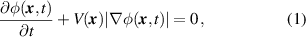
The pseudo-particle model, illustrated in figure 2, tracks individual Monte Carlo pseudo-particles generated with an isotropic distribution on a source plane above the evolving surface with reflective boundary conditions. All pseudo-particles are of the same type and have the same properties. A pseudo-particle interacts with both the photoresist and the  by etching and subsequently reflecting with an isotropic re-emission distribution.
Figure 2. Illustration of the single pseudo-particle model implemented in the topography simulator [34]. The pseudo-particle interacts with both the photoresist and  by etching and reflecting isotropically.
Download figure:
Standard image High-resolution imageThis model is uniquely determined by designating a plane wafer etch rate (PWR) and sticking probability β for each material being either photoresist ( ) or
) or  . In general, sticking probabilities are complex quantities which vary locally, depending on, e.g. the clean surface sticking probability and surface coverages by reactants [21, 32, 40, 41]. For simplicity, we approximate the sticking probability as a constant for each material. This approximation is well-established in the literature and has shown agreement with experiment [42]. Upon intersecting with the surface at point
x
, each particle p adds to the local scalar velocity
. In general, sticking probabilities are complex quantities which vary locally, depending on, e.g. the clean surface sticking probability and surface coverages by reactants [21, 32, 40, 41]. For simplicity, we approximate the sticking probability as a constant for each material. This approximation is well-established in the literature and has shown agreement with experiment [42]. Upon intersecting with the surface at point
x
, each particle p adds to the local scalar velocity  according to

where  is the per-particle flux and
  a per-particle probability. Since p is a Monte Carlo pseudo-particle, its corresponding
  can be interpreted as a weight to the pseudo-particle payload
  . After each reflection, said weight is reduced according to the fixed sticking coefficient. Thus,
  is initialized as 1 for each pseudo-particle generated in the source plane. Upon encountering a surface element, p is terminated and a new, reflected pseudo-particle is generated with probability

The final etch rate is then obtained by combining all particle contributions to the velocity field:
As we show in the following, this model captures the essential characteristics of the low-voltage-bias  etch process described in section 2.1.
  is known to be a source of highly reactive, non-selective F atoms [43, 44] which chemically etch the surface both vertically and laterally [17]. This motivates our use of an isotropic description of the source and re-emission distributions. It also highlights the importance of visibility and reflection effects. These effects underscore the difference in reactant transport between low-voltage-bias plasma etching and isotropic wet etching processes which are also common in micromachining processing [45]. Wet etching processes in the reaction-limited regime are expected to have an equal supply of reactants to the exposed geometry [46], ultimately leading to a different surface.
3.3. Calibration procedure
The pseudo-particle model described in section 3.2 has the plane wafer etch rates PWR and sticking probabilities
  as free input parameters. Additionally, we allow the plane wafer etch rate for Si PWR
 to be different for each etch step, enabling the capture of reactor loading effects. The model thus has five free parameters in total, which are described in table 1. Although some of these parameters can be experimentally estimated we assume that they are free to achieve maximum flexibility. That being said, having five free parameters, a robust calibration procedure to match the simulated geometries to the experimental data, as is illustrated in figure 3, is required.
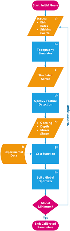
Figure 3. Flowchart representation of the calibration algorithm: it determines the plane wafer etch rates and sticking probabilities by matching the experimental and simulated geometries.
Download figure:
Standard image High-resolution imageTable 1. Definition of the five free pseudo-particle model parameters.
| Free parameter | Definition |
|---|---|
1st PWR
| Plane wafer etch rate of  for 1st step for 1st step |
2nd PWR
| Plane wafer etch rate of  for 2nd step for 2nd step |
PWR
| Plane wafer etch rate of the photoresist |

| Sticking probability of 
|

| Sticking probability of the photoresist |
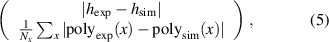
The central challenge of calibrating a topography simulation to experimental data is that of matching geometrical data. From the simulation (cf section 3.1 and figure 3(c)) we obtain a triangle mesh, whereas the characterization procedure described in section 2.2 provides a list of coordinates. We match such disparate data by developing a purpose-built feature detection algorithm and applying it to both experimental and simulated geometries, as shown in figure 3(d)). The underlying method is the circular Hough transform [47], as implemented in the OpenCV library [48]. This method enables the detection of the circle which forms the maximum opening of the experimental and simulated microcavities, delimiting the relevant area. All of the data points are then projected into their radial coordinate, reducing the data set from three to two dimensions. This projection is possible since rotational symmetry is present. We then obtain a functional description of the microcavities by fitting an even sixth-order polynomial to all points on the inside. As summarized in figure 3(e)), after the feature detection procedure, each simulated and experimental geometry is described by their maximum opening diameter O, maximum depth h, and by a mirror shape given by a polynomial  .
.
The calibration procedure requires the definition of a cost function to be minimized, illustrated in figure 3(g)). We define our cost function as the Euclidean norm of a vector of residuals. For each microcavity to be calibrated, we construct the residuals as
where Nx
is the number of samples of x taken from the region inside the microcavity. We calibrate our simulation ( ) simultaneously to m multiple experimentally (
 ) realized microcavities, each with a different photoresist opening d. Since each microcavity contributes with two entries to the vector of residuals, the final vector contains
  entries.
In order to determine the global minimum of the cost function, the generalized simulated annealing (GSA) algorithm is employed [49], as implemented in the SciPy library [50, 51] (cf figure 3(h)). Since our topography model is based on a Monte Carlo method [37], our cost function is susceptible to random variations after slight changes in input parameters. That is, our minimization landscape is noisy with respect to local searches in the parameter space. Therefore, we employ the GSA algorithm to minimize our cost function. The GSA algorithm enables larger jumps in the parameter space and searches more efficiently, in our case, compared to other algorithms available in SciPy.
The calibration approach is performed, as discussed in section 4.1, on m = 3 microcavities. The lateral extent of the simulation domain is 160 µm × 160 µm with a finite difference grid spacing of 0.5 µm. The number of Monte Carlo pseudo-particles per time step is of approximately 6.1 million (120 pseudo-particles per source plane grid point). The optimization is performed using a dual-socket compute node equipped with dual Intel Xeon Gold 6248 processors (40 physical computing cores in total). Since each mirror can be calculated independently and simultaneously, each simulation is assigned 13 threads in order to evenly distribute the workload over the 40 computing cores. The total runtime depends greatly on the chosen parameter value bounds, particularly on the plane wafer etch rates. A typical GSA run with 100 iterations requires approximately 60 hours.
4. Results and analyses
4.1. Model calibration
Following the procedure described in section 3.3, we calibrated our pseudo-particle model to three microcavities with d of: 12.4 µm, 34 µm, and 52 µm. A visual comparison of the calibrated simulation to the profilometer data is summarized in figure 4. The final geometries of each of the three microcavities, obtained by the profilometer according to the procedure described in section 2.2, are the calibration targets for the residuals constructed according to (5). The calibrated parameters are shown in table 2.

Figure 4. Comparison of simulation results to profilometer data for microcavities with initial photoresist opening d of  m,
m,  m, and
  m. The whole three-dimensional geometry is incorporated by considering axial symmetry.
Download figure:
Standard image High-resolution imageTable 2. Calibrated parameters.
| Free parameter | Calibrated value |
|---|---|
1st PWR (µm min−1) (µm min−1) | 2.151 |
2nd PWR (µm min−1) (µm min−1) | 0.661 |
PWR (µm min−1) (µm min−1) | 0.209 |
 (-) (-) |

|
 (-) (-) |

|
| Cost function (µm) | 0.367 |
The calibrated PWR and
and  shown in table 2 are consistent with values reported from the literature [45, 52–54]. The
  reduction of PWR
 during the second etch step is consistent with the loading effect [17, 55, 56]. After the removal of the photoresist, there is a larger available area of the
  to be consumed by the reactants. This locally reduces the availability of reactants, decreasing the etch rate. Additionally, a photoresist selectivity of approximately 10 to 1 is consistent with reported results [52, 57, 58].
4.2. Resonator parameter extraction
As described in section 1, the goal of manufacturing these cavities is the production of optical resonators [10]. For our analysis, we therefore consider that the resonator is assembled in a plano-concave geometry (cf figure 5). Two additional parameters are then extracted from the simulated geometry arising from the calibrated parameters presented in section 4.1: the ROC and the beam waist size  . The extraction procedure follows the scheme presented in figure 5.

Figure 5. Illustration of the procedure to extract the optical parameters from the simulated microcavities in a plano-concave resonator configuration. (1) After the feature detection algorithm determines the opening (O), (2) the radius of curvature (ROC) is extracted. Subsequently, (3) the waist ( ) and (4) the polynomial description of the cavity are determined.
Download figure:
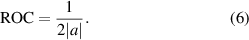
Standard image High-resolution imageFirstly, the feature detection algorithm presented in section 3.3 outputs a detected opening O. From O, we extract a representative ROC of the resonator by fitting a parabola  in the region inside
  of the final opening. By focusing on a central and relatively small region, the extracted parameters are accurate and still representative of the global characteristics. The ROC is then:
For resonators in the plano-concave configuration, the Gaussian beam waist size at the concave mirror  is given by [59]
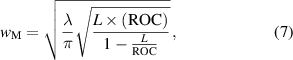
where L is the resonator length and λ a representative wavelength. Here, we assume that the ratio  and that the relevant wavelength is
  m, which are the values obtained from further infrared laser analysis of assembled resonators [10].
The  can be interpreted in a Gaussian sense as one standard deviation σ of the beam relative to its center of symmetry. This motivates us to define the region of interest as
  , or equivalently, 3σ. This represents enough area such that the maximum possible finesse, which is a quantity to measure losses inside the resonator, is larger than 107 [60, 61]. Therefore, we extract a functional description of the microcavity by fitting a sixth-order even polynomial to the region inside either of
  or the detected opening O, whichever is smallest.
4.3. Process parameter optimization
Based on the calibrated parameter set different etch time scenarios can be accurately investigated. The devices fabricated as described in section 2.1 were etched with the photoresist for  s for a cumulative etch time
  s. Our approach allows for investigating possible states of the topography for different etch times, not only for intermediate periods during the executed etch but also for alternative etch time configurations. This highlights how our modeling approach is able to provide detailed insights which would have otherwise required numerous additional experiments. This approach is valid under the moderate assumptions that the reactor conditions, as reflected in the plane-wafer etch rates and sticking probabilities, are constant during each step [28].
The evolution of selected geometric features of a microcavity with a photoresist  m is depicted in figure 6. We observe that
  directly defines the h of the microcavity. This is expected, as after the removal of the photoresist the whole wafer is exposed to the reactor and there is comparatively little variation in local etch rates. The opening O is influenced by both etching steps; however, the rate of increase of O is influenced by
  . Interestingly, the ROC has its minimum defined by the first etch step, reaching a global minimum near
  s. Since a small ROC is a desired attribute of the device, this indicates that the second etch step should be kept as short as possible.

Figure 6. Time evolution of (a) maximum depth (h), (b) maximum opening (O), and (c) ROC for simulated cavities with an initial photoresist opening diameter  m. The blue line represents the evolution during the first etch step with the photoresist present. The remaining lines show the evolution of the geometry for different total first etch steps (
 ). The same extraction methodology is applied to the manufactured mirror and is shown with label 'Experiment' for comparison.
Download figure:
Standard image High-resolution imageThe noise observed in the extracted geometrical features is a consequence of our simulation engine using a Monte Carlo method [37]. Nonetheless, we highlight that our simulations match the experimental data when applying the same geometrical feature extraction procedure described in section 4.1 to the experimental topography.
4.4. Scale analysis
Scale analysis is a procedure to determine whether the process evolution characteristics scale with a particular geometric parameter. We are interested in determining if the processing characteristics scale with the main geometric input: the photoresist d. We achieve this by dividing both the etch time  and an output variable, such as the ROC, by d. With the scale analysis, we can evaluate if higher or lower values of d lead to resonators of higher quality.
As it can be seen in figure 7, our simulations show that the scaling curves for all three microcavities have similar shapes. This shows that the process, under the conditions described in section 2.1, scales directly with d. Therefore, we expect that other geometrical scales, such as the thickness of the photoresist or the aspect ratio of its cylindrical hole, do not play a significant role, otherwise, the curves in figure 7 would not match. From this analysis, we expect that the resonator finesse is further optimized by minimizing the ROC by decreasing the photoresist d.
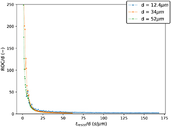
Figure 7. Scaling behavior of the ROC of the simulated cavities after the first etch step. Both the ROC and the length of the first etch step ( ) are scaled with the respective initial photoresist opening diameter (d) for each of the three simulated microcavities.
Download figure:
Standard image High-resolution image4.5. Optimization of design criteria
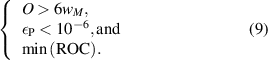
Our modeling and simulation approach enables us to investigate how the etch times affect the quality of the microcavities, allowing for design optimizations. Consequently, it is important to define objective design criteria through which we evaluate the quality of a microcavity: to that end, firstly, we expect the final opening O to be large enough to contain most of the beam. For this purpose, we require O to be larger than six times  defined in (7). From a Gaussian beam analysis point of view, this value of O is sufficient to contain three standard deviations of the intensity of the beam inside the resonator. This is enough to obtain resonators with potential finesse larger than the state of the art [10].
Secondly, the best performance of the resonators is obtained when the cavity shape is as parabolic as possible [62]. We model the shape of the microcavity by an even polynomial. We find that a sixth-order polynomial fit  , as described in section 4.1, is sufficient, since we seek to manufacture parabolic cavities. Therefore a sixth-order fit suffices to both match the simulated geometry and quantify deviations from the ideal parabolic behavior. We then define our measure of parabolicity P as:
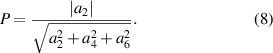
This motivates defining the parabolicity error as  . We set a maximum
  threshold to 10−6, which is adequate to generate resonators with finesse larger than 106 [60].
Thirdly and lastly, as already discussed in section 4.3, the ROC should be as minimal as possible. Therefore, our optimization targets are summarized as follows:
The simulation results for the cavity with photoresist  m are summarized in figure 8. From figure 8(a)), we see that the cumulative etch time required for the design criterion on the opening O is significantly reduced with increased
  . This design criterion, shown by a blue arrow in figure 8(a)) will already be fulfilled with the photoresist on at time
  s. Combining this insight with the reduction in ROC seen in figure 6, we see good evidence for increasing the
  to approximately its double in order to minimize the ROC and achieve a sufficiently large O quickly. However, it must be noted that
  cannot be arbitrarily increased due to experimental limitations. Possible issues are photoresist hardening [45, 63] and loss of photoresist structural integrity after significant underetching.

Figure 8. Time evolution of (a) beam waist ( ), and (b) parabolicity error (
 ) for simulated cavities with an initial photoresist opening diameter
  m. The arrows indicate the times when the design criterion
  is met. The error threshold is set to 10−6.
Download figure:
Standard image High-resolution image
Analyzing the  in figure 8(b)), we highlight the necessity of the second etch step. After the first step, the microcavities have very poor P. It is during the second etch step that we see an improvement of the
  . The aforementioned behavior is explained by the second etch step being essentially isotropic without any visibility effects, as illustrated in figure 1(a)). During such an isotropic process, we see that the feature converges to a parabola. This behavior exposes a fundamental trade-off on increasing the second etch time: whereas it improves the
  , it also worsens the ROC. Our analysis suggests that the second etch time should be kept as short as possible, which keeps the
  under a fixed threshold. We thus expect that microcavities of comparable quality are achieved with a reduction of up to
  of the second etch duration. Combined with the analysis from the first etch step, this results in an overall reduction in etch time of at least
  , representing a significant optimization of microcavity plasma etching processes.
5. Conclusion
We present a modeling and topography simulation approach and use it to analyze the fabrication of  microcavity resonators using
  plasma. Alongside the applied pseudo-particle model, we develop a novel and robust calibration procedure in order to match the simulations to the experimental data. Such calibrated simulations enable us to simultaneously optimize the etch times and the photoresist opening diameter without complex reactor modeling and go beyond conventional statistical process modeling. By using calibrated simulations, we are able to analyze and obtain new insights into optimizing microcavities with respect to the plasma etching processing steps.
In essence, our work provides guidance for optimizing microcavity fabrications by exploring processing parameters. We base our investigations on a reference two-step etching process, both with respect to calibration but also concerning process optimizations. The resonator quality, defined in our work by minimizing the  P
, is improved by increasing
P
, is improved by increasing  by a factor of 2. However, attention has to be placed on keeping excessive underetching and photoresist structural stability under control. Furthermore, the second etch step can be reduced by
  , leading to a
  reduction of
  and, consequently, a reduction in process cost and complexity. Additionally, our scaling analysis shows that the ROC is further optimized by reducing the photoresist d.
Acknowledgments
The financial support by the Austrian Federal Ministry for Digital and Economic Affairs, the National Foundation for Research, Technology and Development and the Christian Doppler Research Association is gratefully acknowledged. The computational results presented have been achieved in part using the Vienna Scientific Cluster (VSC). M Trupke and G Wachter gratefully acknowledge support from the EU H2020 framework programme (QuanTELCO, 862721), the FWF (SiC-EiC, I 3167-N27), and the FFG (QSense4Power, 877615). The authors acknowledge TU Wien Bibliothek for financial support through its Open Access Funding Programme.
Data availability statement
The data that support the findings of this study are available upon reasonable request from the authors.