

Abstract
Lead (Pb) nanowire arrays were fabricated with anodic aluminum oxide (AAO) templates of 30, 100 and 300 nm in pore diameters. Through vacuum injection molding process, Pb/AAO composite was obtained, and lead sulfide (PbS) could further be synthesized after exposing to sulfur gas. AAO templates with different pore sizes were fabricated by using pure aluminum in a two-step anodization. Three types of solutions, which are 10 vol% sulfuric acid, 3 wt% oxalic acid and 1 vol% phosphoric acid, were adopted to achieve AAO of various pore sizes. Different sulfurization temperatures and time spans were applied for studying on the formation mechanism of PbS. Finally, the morphology, composition, structure and elements distribution of the as-prepared Pb and PbS nanowires were confirmed through the use of scanning electron microscopy, energy dispersive x-ray spectroscopy, element-mapping, x-ray diffraction and transmission electron microscopy analysis. The results indicated that Pb nanowires were successfully obtained after applying vacuum injection molding process with 50 kgf cm−2 hydraulic pressure, and PbS nano arrays can be formed by sulfurization at 500 °C for 5 h. Furthermore, an optical property, ultraviolet–visible (UV–Vis) absorption, was also measured. The measurement of the PbS nanowires showed that a significant quantum confinement effect made the energy gap produce a blue shift from 0.41 eV to 1.65 eV or 1.72 eV.
Export citation and abstract BibTeX RIS
1. Introduction
There has been an increasing interest in low dimensional semiconductor nanostructures, which have been the building blocks of many new technologies in fields such as electronics, optoelectronics and biology [1–5]. These low dimensional structures are interesting because they can be manipulated by controlling their structure and chemistry, a characteristic which differs from those of the bulk. For example, the energy gap of ZnS nanocrystals increases from 3.68 to 4.37 eV when their size is decreased from bulk regime to 2– 5 nm [6]. Another difference is their large surface-area-to-volume ratio. For instance, Yi et al fabricated well-aligned ZnO nanorod (NR) arrays which were grown on the indium-tin-oxide glass through a hydro-thermal method to create high-performance ultraviolet (UV) photodetectors with a photocurrent of ∼308.04 μA, an on/off ratio of ∼5.13 × 10², and a fast decay time constant of 1.69 s at 1 V applied bias. The performance of the ZnO NRs device was much better than that of the conventional ZnO film device [7]. Consequently, nanostructured semiconductor materials with desired properties can be produced by manipulating their dimensions, structure and chemical composition. Various semiconductor nanomaterials have been synthesized, and many extraordinary properties have been unfolded. Lead sulfide (PbS) is a typical semiconductor with a rock-salt crystal structure (FCC), and it possesses a rather small band gap with Eg = 0.41 eV at 300 K [8] and a relatively large excitation Bohr radius of 18 nm [9]. It also shows shape flexibility and shape evolution features in the nanoscale regime [10–12]. Tuning the band gap of PbS by size and shape manipulation has rendered PbS useful in various applications. For example, PbS nanomaterials have been successfully applied as promising candidates for fabricating gas sensors. Kaci et al synthesized PbS thin films by modified polyol process on amorphous a-SiC and p-Si(100) substrates, which exhibited highly sensitive with fast response to H2 [13]. Song et al synthesized star-shaped PbS nanomaterials and further assessed their gas sensing properties such as sensitivity and response-recovery in ethanol detection [14]. Jahromi et al proposed and fabricated a highly sensitive solid-state acetone sensor based on lead sulfide nanosheets [15]. Furthermore, it can also be utilized in light-emitting diode [16, 17], Optical waveguides [18], optical fiber amplifiers [19], photon detectors [20, 21], IR detectors [22], display devices [23], and solar cells [24–26]. PbS nanocrystals with various morphologies such as nanoparticles [27], quantum dots [28], thin film [29], nanosheet [15], hollow spheres [30], wires [31, 32], rods [33, 34], tubes [34], hierarchical structures [35] and star-like structures [36] have also been synthesized nowadays with gas, liquid and solid approaches.
As technology requirements increase, highly crystalline nanowires have attracted extensive attentions in the solar cell field, because they can provide direct conduction channels and be used as highways for electron transport due to the absence of grain boundaries [37]. Xu et al reported that highly crystalline nanowires can replace the disordered structure of mesoporous TiO2 films used in current dye-sensitized solar cells (DSCs) with vertically aligned 1D nanostructures directly on transparent conducting oxides to increase the energy conversion efficiency of DSCs [38]. Therefore, the methods for precisely controlling and predicting 1D nanostructure growth has been a primary topic of study in the field of optics. However, the methods used to prepare the 1D nanostructure of PbS usually requires multi-step routes in the preparation process, and some special precursors might need to be prepared in advance. Toxic surfactants and ligands are sometimes used as additives, which are harmful to the environment and human body. In addition, because PbS is a material with three-dimensional isotropic structure, it is difficult to be formed into a one dimensional structure [39].
Here, we attempt to use anodic aluminum oxide (AAO) as a template to grow 1D nanomaterial. AAO is a typical template for synthesizing derivative nanomaterials. It possesses many unique features, such as high aspect ratio, uniform pore size, and high structural order. It is also environmentally friendly and has chemical stability and thermal stability [40]. In our previous work, we developed a facile approach for growth of ZnO nanowires (NWs) via using AAO templates with the assistance of vacuum injection molding process. Two-step anodizing method has been employed for the fabrication of AAO templates. With a constant voltage of 45 V for 1 h at 20 °C during 1st anodization and the second anodization was carried with the same condition as the first step for 24 h and thus resulted in the highly ordered AAO templates. ZnO NWs with high crystallinity, high homogeneity, and high aspect ratio can be obtained through this process [41].
In this paper, we propose a simple, facile, economical and reproducible method for the fabrication of PbS NWs in AAO templates. First, molten Pb is uniformly embedded in AAO templates through the application of vacuum injection molding process. Then, through a sulfurization process, PbS NWs are formed through the reaction of Pb with sulfur gas under various sulfurization time spans and temperatures. Finally, highly crystalline PbS NWs that are uniform in size are successfully obtained. The relationship between the nanostructure and their formation mechanism is also discussed.
2. Experimental procedures
2.1. AAO template fabrication
AAO membranes can possess two different morphologies: nonporous-type and porous-type. Which one will be formed depends on the chemical nature of electrolytes. Generally, nonporous AAO membranes are formed in neutral electrolytes (pH 5–7). However, in acidic electrolytes, such as sulfuric, oxalic, phosphoric, and etc, porous AAO membranes are formed. In this paper, we chose sulfuric, oxalic, phosphoric acids as our electrolytes. First, the surface roughness of aluminum foil was flattened by mechanical polishing. Then, it was annealed in an air furnace at 550 °C for 1 h. In order to obtain a smooth, uniform and defect-free surface, the Al substrate was electropolished in a bath consisting of 15 vol% HClO4, 15 vol% C2H6O, and 70 vol% CH3(CH2)3OCH2CH2OH with 40 V DC for 30 min. Due to pore diameter is proportional to the applied voltage and base on our findings. After the above pretreatments, the first anodization process was conducted by applying a voltage of 20 V in 10 vol% sulfuric acid solution (H2SO4, 98%) at 5 °C for 1 h. The obtained substrate was soaked in a solution of 1.8 wt% CrO3 and 6 vol% H3PO4 at 70 °C for 1 h to remove the resulting porous AAO layer with disordered pores in its top part to obtain textured aluminum with array patterns of almost hemispherical concaves. The second anodization was carried out under the same conditions, but for a longer time (usually more than 24 h) to form AAO films of varying thickness. In addition, the as-prepared substrate was soaked in a solution of 8 wt% CuCl2 and 5 vol% HCl to remove the residual Al to get the AAO template. Finally, to widen the pore diameter of the AAO template, it was immersed in a 6 vol% H3PO4 solution for 10 min. In the steps above, if the voltage and electrolyte are altered to 50 V and 3 wt% C2H2O4 during the anodization process, and the pore widening time is changed to 30 min, an AAO template with a pore size of 100 nm is formed. Furthermore, if the voltage and electrolyte are altered to 170 V and 1 vol% H3PO4, and the pore widening time is changed to 60 min, an AAO template with a pore size of 300 nm can be obtained.
2.2. The preparation of PbS NWs
The PbS NWs were fabricated by applying vacuum injection molding process and sulfurization process on AAO templates. First, Pb pellets were placed above the AAO template inside a vacuum chamber (figure 1(a)). After the chamber was heated to 360 °C (the melting point of Pb is 327.5 °C) for 10 min, 50 kgf cm−2 hydraulic force was applied to inject the molten Pb into the AAO template. Second, the Pb/AAO composite material was put in a quartz tube together with sulfur powder and sulfurized in a furnace (figure 1(b)) for different time spans (3 h, 5 h and 10 h) at various temperatures (300 °C, 400 °C, 450 °C, 500 °C and 550 °C) to form the PbS/AAO composite. Then, the PbS NWs were released from the AAO by a chemical etching method. Finally, high purity homogeneous crystalline PbS NWs were obtained. Their morphologies were observed with scanning electron microscopy (SEM, JEOL JSM-7900F). The compositions and crystallization of NWs were examined with energy dispersive x-ray spectroscopy (EDS, EDAX) and x-ray diffraction (XRD, Bruker, D2 PHASER).
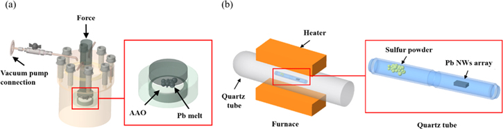
Figure 1. Drawings of (a) vacuum injection molding process and (b) sulfurization treatment of Pb/AAO composite material.
Download figure:
Standard image High-resolution image3. Result and discussion
3.1. Characterizations of lead sulfide NWs in the AAO templates
The morphologies and compositions of the as-prepared AAO template and Pb/AAO were identified with the scanning electron microscopic and the energy dispersive spectrometer (EDS). Figure 2(a) is the SEM image of top view of an AAO template in which pore diameter was 30 nm. Figure 2(b) shows that the Pb NWs formed as hydraulic pressure enforced the molten Pb into the AAO nanomold. From figure 2(c), the cross-section view reveals that the sufficient time and temperature of Pb in vacuum injection molding allowed molten Pb to occupy deeper into the nanochannels. The EDS data in figure 2(d) shows that Pb, O and Al elements were detected, with higher signals of Al and O, because most of the Pb was embedded in the AAO template.
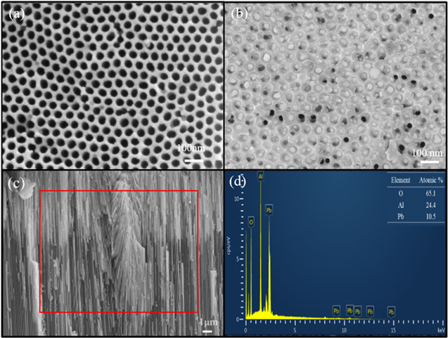
Figure 2. SEM images of (a) top view of the AAO template, (b) top view of Pb/AAO composite, (c) cross-section view of the Pb/AAO composite and (d) EDS data of Pb NWs of the Pb/AAO composite.
Download figure:
Standard image High-resolution image3.2. Reaction of lead NWs and sulfur gas
The influences of different sulfurization time spans and temperatures on Pb NWs were investigated. In the thermodynamics of equilibrium, the state function of Gibbs free energy (G) is a simple way to determine whether a reaction can react spontaneously under a specific temperature and pressure. The following equation can be used to calculate the difference of Gibbs free energy ( of a reaction in any temperature if ignoring the influence of temperature on
  and
and 

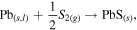
The top right symbol 'ø' means it stays in standard state. The bottom right symbol 'm' means advancement of reaction is 1 mol. The bottom right symbol 'γ' means reaction. From the thermodynamics aspect, the Standard Gibbs Free Energy Changes for PbS formation can be written as [42]:

Based on the thermodynamic calculation, the Gibbs free energy G are −112.76 kJ mol−1, −103.96 kJ mol−1, −99.55 kJ mol−1, −95.15 kJ mol−1, −90.75 kJ mol−1, −81.95 kJ mol−1 as the temperature reaches 300 °C, 400 °C, 450 °C, 500 °C, 550 °C and 650 °C respectively. Since the values of reaction Gibbs free energy are all negative, the reaction is spontaneous at these specific temperatures. All of the Pb NWs would be transformed into PbS crystals if the reaction time is long enough. The growth rate of PbS NWs in the template was significantly affected by the sulfurization parameters. The XRD spectrum of Pb NWs of different diameters is shown in figure 3(a). As shown in figure 3(b), the temperature was fixed at 300 °C, which is lower than the melting point of Pb, for different sulfurization time spans (3 h, 5 h and 10 h), and the XRD spectrum shows that the PbS phase appears under 300 °C for 3 h, but the diffraction intensities are lower than Pb. Furthermore, it also reveals that there is no obvious difference in the intensities of PbS and Pb from 3 h to 10 h. According to the thermodynamic theory, the sulfurization rate can be accelerated by increasing the temperature. As the temperature is increased, the material's thermal vibrational energy, reaction ability and diffusion rate are enhanced. For chemical reaction, the rate constant can be estimated by the equation:  As indicated in this equation, the activation energy is (
 and A is a pre-exponential factor that is related to the activation mechanism. For diffusion, the diffusion coefficient can be estimated by the equation:
  As mentioned, the values of rate constant (
 ) and diffusion coefficient (D) are all increased by increasing the reaction temperature. Temperature causes a higher effect on chemical reaction rate than diffusion because diffusion activation energy (Q) is usually lower than activation energy (
 ). Thus, as shown in figure 3(c), the intensity of PbS is already higher than Pb because the state of Pb is turned solid into liquid when the sulfurization temperature is 400 °C, and the convection effect between Pb and sulfur gas increased, improving the chemical reaction. Besides, the diffraction peaks which were assigned to (111), (200), (220), (311), (222), (400) and (331) planes of a face-centered-cubic structured PbS were observed. The diffraction intensity difference between PbS and Pb is more obvious and the FWHM of diffraction peaks of (111) and (200) decreased when the temperature reached 450 °C, which is higher than the boiling point of sulfur, because it occurred much sulfur gas to facilitate the fabrication of PbS. However, the diffraction intensity of PbS is higher than Pb under 450 °C for 5 h but the Pb still could not be transferred into PbS completely, probably because the temperature was not high enough. Thus, when the temperature was increased to 500 °C, no other peaks of Pb are observed, suggesting pure PbS is obtained. The sharp and strong intensity of XRD peaks suggest that the samples have high crystallinity, as displayed in figure 3(d). The FWHM of diffraction peaks of (111) decreased from 0.1623° to 0.1472° gradually as the temperature was increased from 400 °C to 650 °C. This is because the increase in temperature allows the atoms to have enough energy to release stress through migration and diffusion, thereby improving the crystallinity.
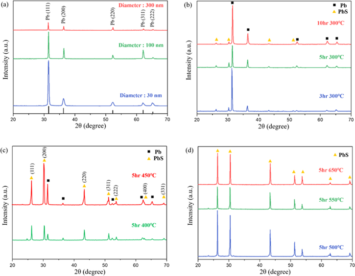
Figure 3. X-ray diffraction profile analyses of (a) Pb wires of different diameters, (b) Pb wires at 300 °C with different sulfurization time spans, (c) Pb wires with different time spans and temperatures and (d) Pb wires at different sulfurization temperatures for 5 h.
Download figure:
Standard image High-resolution imageFigure 4(a) shows that the morphology of PbS/AAO composite with 5 h sulfurization time at 500 °C. There are a lot of PbS nanocrystals grow outside the pores of the AAO templates, as shown in figure 4(b). Then, the PbS/AAO composite was immersed in an acid solution containing 20 vol% of H3PO4 for various time spans at room temperature to remove the AAO film on the surface. As shown in figure 4(c), the tips of PbS NWs are clearer than figure 4(a) after immersing in the acid solution for 30 min. And figure 4(d) shows that the PbS NWs are more obvious after immersing in the acid solution for 6 h. It also proves that the PbS NWs can be obtained from the PbS/AAO composite by a chemical etching method.
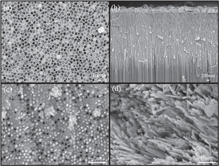
Figure 4. SEM images of (a) top view of PbS/AAO composite, (b) cross-section view of PbS/AAO, (c) PbS/AAO composite was immersed in 20 vol% H3PO4 for 30 min and (d) PbS/AAO composite was immersed in 20 vol% H3PO4 for 6 h.
Download figure:
Standard image High-resolution imageTo further confirm whether the whole nanowires are of the same structure, the morphology and structure of the PbS nanowire which was treated in 500 °C for 5 h was observed by TEM images. As shown in figure 5, there are light and dark contrast regions in the TEM image of the nanowire. The Zone axis of the light-colored region is [01 ] in which there are several planes in this direction, including (111), (0
 ) and (3
 ) planes were confirmed through selected area electron diffraction. From the HRTEM image (figure 6(a)), it can be seen that the fringe spacing are about 0.3483, 0.2128 and 0.1828 nm which corresponding to the interplanar spacing of (111), (0
 ) and (3
 ) planes of the face-centered-cubic structured PbS. As shown in figure 6(b), the Zone axis of the dark-colored region is also [01
 ], and in this direction also contains same planes as the light-colored region. The fringe spacing are about 0.3537, 0.2179 and 0.1859 nm which corresponding to the interplanar spacing of (111), (0
 ) and (3
 ) planes. Therefore, the results further confirms that both the light and dark contrast regions are face-centered-cubic structured PbS, indicating that the NWs prepared by vacuum injection molding process and sulfurization are of the same structure.
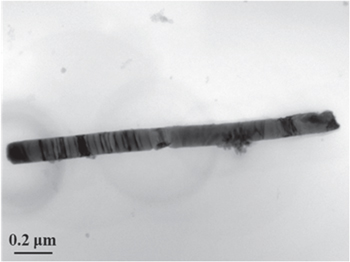
Figure 5. TEM image of a PbS nanowire after sulfurization at 500 °C for 5 h.
Download figure:
Standard image High-resolution image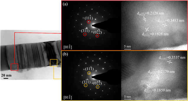
Figure 6. SAED and HRTEM images of a PbS nanowire of (a) light-colored region and (b) black-colored region.
Download figure:
Standard image High-resolution image3.3. Sulfurization mechanism of lead sulfide
The plausible sulfurization mechanism of the formation of PbS on Pb/AAO composites, which complies with the thermodynamic theory, is illustrated as figure 7. We assume that the sulfurization reaction began from the top (marked in red) of the Pb/AAO composite and then proceeded to the bottom (marked in blue), because the bottom of the AAO structure is a condense barrier layer which can almost keep the sulfur gas from flowing in. When the temperature reached 95 °C, the sulfur powders started to transfer into gas. Then the sulfur gas was adsorbed by the Pb and occurred reaction with each other to form nucleus of PbS crystal on the surface. As time goes on, the film of PbS is forming gradually. Because this film prevented the molecules of sulfur gas from reaching the inner Pb, it needed to depend on the interface reaction not only between Pb and PbS but also between PbS and the molecules of sulfur gas to do further sulfurization inside. On the other hand, it depended on the diffusion between the molecules of sulfur gas and PbS film. Thus, PbS phase appears under 300 °C, but the diffraction degree is low. When the temperature was increased to 450 °C, the state of Pb changed from solid to liquid, stimulating the convection between Pb and sulfur gas and, as a result, the PbS formed faster and deeper in the AAO pore. Finally, when the temperature was increased over 500 °C, the Pb was sulfurized into PbS.
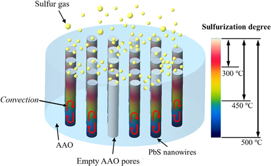
Figure 7. Plausible sulfurization mechanism of the Pb/AAO template.
Download figure:
Standard image High-resolution imageTo confirm that the sulfurization parameters could be used to fabricate the PbS NWs with uniform composition, a chemical etching process using 20 vol% H3PO4 solution was applied to release the PbS NWs from the AAO. After the AAO was dissolved, the solution containing PbS NWs was centrifuged to make the PbS NWs settle in the bottom. Then, elemental mapping analysis and EDS analysis was conducted on the as-prepared PbS NWs, now free of AAO contaminants. Si signals were detected because we put the solution containing clusters of PbS NWs on a silicon substrate. The atomic number ratio of Pb to S is 1.65 when the sulfurization temperature is 300 °C, indicating that the material has not been completely transformed into PbS. This result can also be seen from figure 3(b) that the XRD patterns at this temperature still has Pb diffraction peaks. When the temperature was increased from below the melting point of lead metal to the over-melting point (from 300 °C to 500 °C), it can be found that the ratio of Pb to S becomes more and more close to 1 as the temperature rises. Moreover, according to the XRD analysis in figure 3(d), the diffraction peaks of Pb cannot be observed at the temperature of 500 °C. The ratio of Pb to S is approximately 1:1 at 500 °C for 5 h, and the elements of Pb and S are distributed evenly, as shown in figure 8, to further verify the Pb NWs were sulfurized completely to form PbS NWs. The EDS results of different sulfurization parameters were listed in table 1.
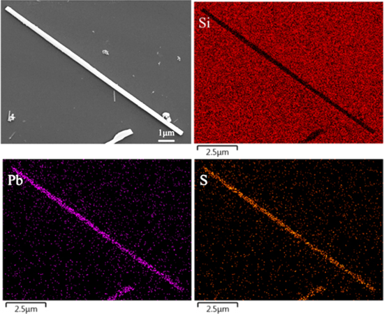
Figure 8. Elemental mapping of single PbS NW.
Download figure:
Standard image High-resolution imageTable 1. EDS analysis of different sulfurization parameters.
| Parameter | Element | ||
|---|---|---|---|
| Pb (at%) | S (at%) | Ratio | |
| 5 h_300 °C | 62.3 | 37.7 | 1.65 |
| 5 h_400 °C | 60.9 | 39.1 | 1.55 |
| 5 h_450 °C | 54.4 | 45.6 | 1.19 |
| 5 h_500 °C | 50.7 | 49.3 | 1.02 |
3.4. Optical properties of PbS NWs
PbS is an excellent semiconductor material because of its narrow band gap ∼0.41 eV and a large excitation Bohr radius of 18 nm. Quantum confinement of both charge carriers can be easily achieved by fabricating PbS with nanosize radius. The ultraviolet–visible (UV–Vis) absorption spectra of PbS NWs of 30 and 100 nm in diameters, shown in figure 9, were measured from 600 to 900 nm at the room temperature. Figure 9 indicates that the two different diameters of PbS NWs have their peaks at about 750 and 720 nm. The probable explanation for the energy gap of PbS NWs shift from 0.41 to 1.65 eV or 1.72 eV is indicative of the presence of the quantum confinement effect.

Figure 9. Ultraviolet–visible (UV–Vis) absorption spectra of PbS nanowires.
Download figure:
Standard image High-resolution image
4. Summary
In conclusion, a method to fabricate PbS NWs have been developed. They are synthesized from the reaction between Pb NWs and sulfur gas. According to the results of x-ray diffraction, PbS NWs are formed effectively at 400 °C for 5 h because higher temperature and convection of molten Pb enhance the chemical reaction. With optimized sulfurization parameters such as temperature and time, we precisely control the PbS NWs growth inside the AAO templates. PbS NWs with high crystallinity and size uniformity were successfully obtained. The UV–Vis absorption measurement describes the absorbance of light energy of PbS NWs. Two broad absorbance peaks around 750 and 720 nm were observed. Such a large blue shift from 0.41 eV (band gap of the bulk) to 1.65 eV or 1.72 eV indicates a significant amount of quantum confinement energy. Overall, this research presents an improved method to overcome pre-existing drawbacks of chemical synthesis, such as complicated and time-consuming processes, and the use of toxic surfactants, in the hopes that it can give rise to alternative methods of producing PbS NWs and expand the possibility of related optical applications.
Data availability statement
All data that support the findings of this study are included within the article (and any supplementary files).