Article

Highly Stable Inverted CdSe/ZnS-Based Light-Emitting Diodes by Nonvacuum Technique ZTO as the Electron-Transport Layer

1
Joint International Laboratory of Information Display and Visualization, School of Electronic Science and Engineering, Southeast University, Nanjing 210096, China
2
The Key Laboratory of MEMS of the Ministry of Education, School of Electronic Science and Engineering, Southeast University, Nanjing 210096, China
3
Institute of Microscale Optoelectronics, Shenzhen University, Shenzhen 518000, China
*
Authors to whom correspondence should be addressed.
These authors contributed to the manuscript equally.
Electronics 2021, 10(18), 2290; https://doi.org/10.3390/electronics10182290
Submission received: 13 August 2021 / Revised: 5 September 2021 / Accepted: 7 September 2021 / Published: 17 September 2021

Abstract

:
CdSe/ZnS quantum dots (QDs) have attracted great consideration from investigators owing to their excellent photo-physical characteristics and application in quantum dot light-emitting diodes (QD-LEDs). The CdSe/ZnS-based inverted QD-LEDs structure uses high-quality semiconductors electron transport layers (ETLs), a multilayered hole transporting layers (HTLs). In QD-LED, designing a device structure with a minimum energy barrier between adjacent layers is very important to achieve high efficiency. A high mobility polymer of poly (9,9-dioctylfluorene-co-N-(4-(3-methylpropyl)) diphenylamine (TFB) was doped with 4,4′-bis-(carbazole-9-yl) biphenyl (CBP) with deep energy level to produce composite TFB:CBP holes to solve energy mismatch (HTL). In addition, we also improved the QD-LED device structure by using zinc tin oxide (ZTO) as ETL to improve device efficiency. The device turn-on voltage Vt (1 cd m−2) with ZTO ETL reduced from 2.4 V to 1.9 V significantly. Furthermore, invert structure devices exhibit luminance of 4296 cd m−2, current-efficiency (CE) of 7.36 cd A−1, and external-quantum efficiency (EQE) of 3.97%. For the QD-LED based on ZTO, the device efficiency is improved by 1.7 times.

Graphical Abstract

1. Introduction

In recent years, Quantum dots (QDs) have attracted considerable attention as an active material because of their excellent optoelectrical properties, such as broadband absorption, bandgap turnability, narrow full-width half maximum (FWHM), high photoluminescence (PL), inherent photo-physical stability, and their advanced optoelectronic application in QD based light-emitting diodes (QD-LEDs) [1,2,3,4,5]. The CdSe/ZnS core–shell is a kind of QD-LEDs that have a wide variety of applications because of their remarkable stability, solution-processability, color tunability, and good efficiency [6,7]. However, there are still some issues that need to be resolved, such as high turn-on (VT) voltage, low device efficiency in the feasible brightness range, and surface trap-states of QDs, which are caused by ineffective carrier injection in the emission layer and a deprived electron–hole balance inside the structure [8,9,10,11]. In general for inverted CdSe/ZnS QD-LEDs, Fluorine-tin oxide (FTO) coated glass has been used as a bottom substrate, zinc oxide nanoparticles (ZnO NPs) act as electron transport layer (ETL), poly(3,4-ethylenedioxythiophene) polystyrene sulfonate (PEDOT:PSS) acts as hole injection layer (HIL) [12,13], poly(9-vinlycarbazole) (PVK) [14] and/or poly[N,Ni-bis(4-butylphenyl)-N,Nibisphenylbenzidine) (poly-TPD) [15,16] are used for hole transporting layer (HTL), CdSe/ZnS QD acts as light-emissive layer (EML), and Au is deposited as top electrode [17,18].
Metal oxides such as zinc tin oxide (ZTO), titanium dioxide (TiO2), and zinc oxide nanoparticles (ZnO NPs) have been utilized as ETLs to enhance electron injection and charge balance in the QD EML [19,20]. In comparison to organic compounds, inorganic compounds such as metal oxides have high thermal stability and resistance to oxygen and moisture. Among several metal oxide ETL materials, solution-processed ZnO NPs outperformed other vacuum-deposited metal oxides in QD-LEDs. There are still some difficulties with solution-processed metal oxide ETLs; through the solution processing of two consecutive layers, an intermix might develop, resulting in a leakage current inside the structure [21,22].
Furthermore, the exciton quenching action may be caused by the hydroxyl bond (O-H) generated during the solution process. As a result, ZTO has been investigated as an ETL material for QD-LEDs to build an efficient inorganic ETL. ZTO’s nature as a compound-based ZnO and SnO2 energy band characteristics have in-between values of ZnO and SnO2, and these qualities might contribute to enhancements in ETL electron transport/injection and hole blocking layer [21]. In contrast to the highest occupied molecular orbital (HOMO) and lowest unoccupied molecular orbital (LUMO) energy levels of conventional conjugated organic molecules or polymers (5.5 and 3 eV, respectively), QDs have a lower valence band (VB) (6 to 7 eV) and conduction band (CB) (4 to 5 eV) energy levels [23,24,25]. Injecting holes from the organic layer into QDs has a high potential energy barrier (greater than 1 eV), but electrons can easily insert into QDs. As a result, the active charge transfer mechanism is hampered, resulting in excessive charge injection. Unbalanced charge injection causes undesirable auger recombination, such as leakage current and device heating, reducing device performance [25].
However, high hole mobility HTLs such as poly(9,9-dioctylfluorene-co-N-(4-butyl phenyl) diphenylamine) (TFB) [26,27] and 4,4í-bis(carbazole-9-yl) biphenyl (CBP) [28,29] were investigated to increase the hole mobility and reduce the potential barrier between the HTL and QD EML, resulting in improved overall device performance [15,30]. Furthermore, it was shown that such composite HTLs could improve hole transport mobility and form a stepwise energy level for hole injection in the device by combining the high mobilities of TFB and the deep-lying HOMO level of CBP, which promotes charge carrier transport balance, reduces multi HTLs into a single layer, and injects holes in QDs [31].
To enhance the device performance, we successfully designed and fabricated the inverted QD-LED by using composite HTL TFB:CBP 4:1 [31] and solution-processed ZTO as ETL. By using these strategies, the charge balance and interfacial interaction among the transporting and active layers were effectively improved. By compiling these ideas, the devices showed a low (VT) of 1.9 V and maximum luminance of 4296 cd m−2 at a current efficiency (CE) of 7.36 cd A−1. We are confident that this structural optimization has laid the groundwork for the design phase of hybrid QD-LEDs and the identification of next-generation QD-LED-based display and lighting technologies that demand high resolution and low production costs.

2. Materials and Methods

2.1. Synthesis

CdSe/ZnS core–shell QDs were synthesized according to the previously reported method with minor modification [32,33,34]. Briefly, 2 mmol of Cadmium Oxide (CdO), 3 mmol zinc acetate, 6 mL Oleic acid (OA), and 25 mL octadecene (ODE) were mixed into a 100 mL round flask, heated to 160 °C, filled N2 with vigorous stirring, degassed and further heated to 280 °C to obtain the clear solution of Cd (OA)2 and Zn (Ac)2. At 280 °C, 0.4 mmol of selenium (Se), 4 mmol sulfur (S) powder dissolved together in 3 mL Trioctylphospine (TOP) for 5 min at 100 °C, were injected rapidly into the reaction flask. After injection was over, the temperature was maintained at 280 °C for 20 min. Then, 0.6 mL dodecanthiol (DDT) was added dropwise at the rate of 1 mL min−1 for another 10 min. Finally, the mixture was cooled to room temperature to produce the red CdSe/ZnS QDs using an ice bar. For purification, acetone and chloroform were added to the suspensions, followed by centrifugation at 10,000 rpm for 10 min and dissolved in octane for further use. ZnO NPs were synthesized according to the reported method [35,36]. ZTO was synthesized according to the following reported articles after some modification [37]. ZnCl2 and SnCl2 were selected as the zinc and tin precursors. Ethanol was used due to its environmentally friendly solvent. The ZnO precursor solution was prepared by dissolving 0.2 M (0.136 g) ZnCl2 in ethanol. 0.2 M (0.225 g) SnCl2 was dissolved in ethanol and stirred at 60 °C to form a SnO2 precursor solution. To form a ZTO precursor solution, we mixed ZnO and SnO2 precursor solution at the molar ratio of 1:1. Before use, the precursor solution was stirred for 2 h and filtered through a 0.22 µm nylon syringe filter.

2.2. Device Fabrication

First, detergent, deionized water, acetone, ethanol, and isopropyl alcohol were used to clean Fluorine-doped Tin oxide (FTO) patterned glass in an ultrasonication bath for 15 min. The ZTO precursor solution as ETL spin-coated at 2000 r/min for 60 s and sintered at 180 °C for 10 min. Then, CdSe/ZnS QD (10 mg mL−1 in octane) was spin-coated on the deposited ZTO layer at 1500 r/min for 30 sec and sintered for 10 min at 120 °C. Afterward, hybrid HTL (10 mg mL−1 in chlorobenzene) TFB:CBP = 4:1 was spin-coated on the QD film at 2500 r/min for 40 sec and annealed at 120 °C for 15 min. In the end, Au (electrode) was deposited by thermal deposition via a shadow mask. Our fabricated device has a 0.04 cm−2 emission zone.

2.3. Device Characterization

Field emission electron microscopy (FESEM, Quanta 200, FEI: Hillsboro, OR, USA) is used to measure the thickness of the layer. Smartlab-3 diffractometer was used to obtain the X-ray diffraction (XRD) results. FEI Tecnai-G20 was used to take tunneling electron microscope (TEM) and the high-resolution (HR) TEM images. UV-vis spectrophotometer (UV-1780, SHIMADZU) was used to measure the absorption of the samples. EDINBURGH(FS5) system used to measure photoluminance (PL) and quantum yield (QY). KEITHLEY 2400 and Spectrascan (PR 670) instruments were used to optimize the optoelectronic properties of the QLED device. The optimizations were carried out under an ambient atmosphere.

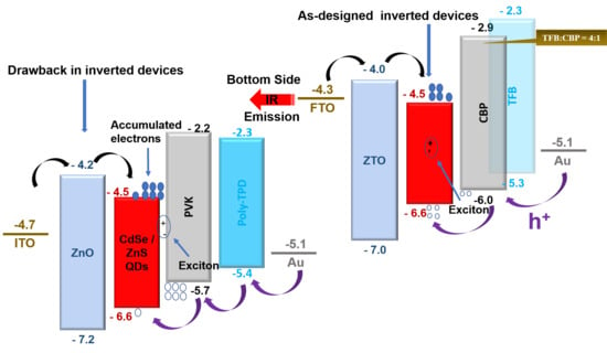
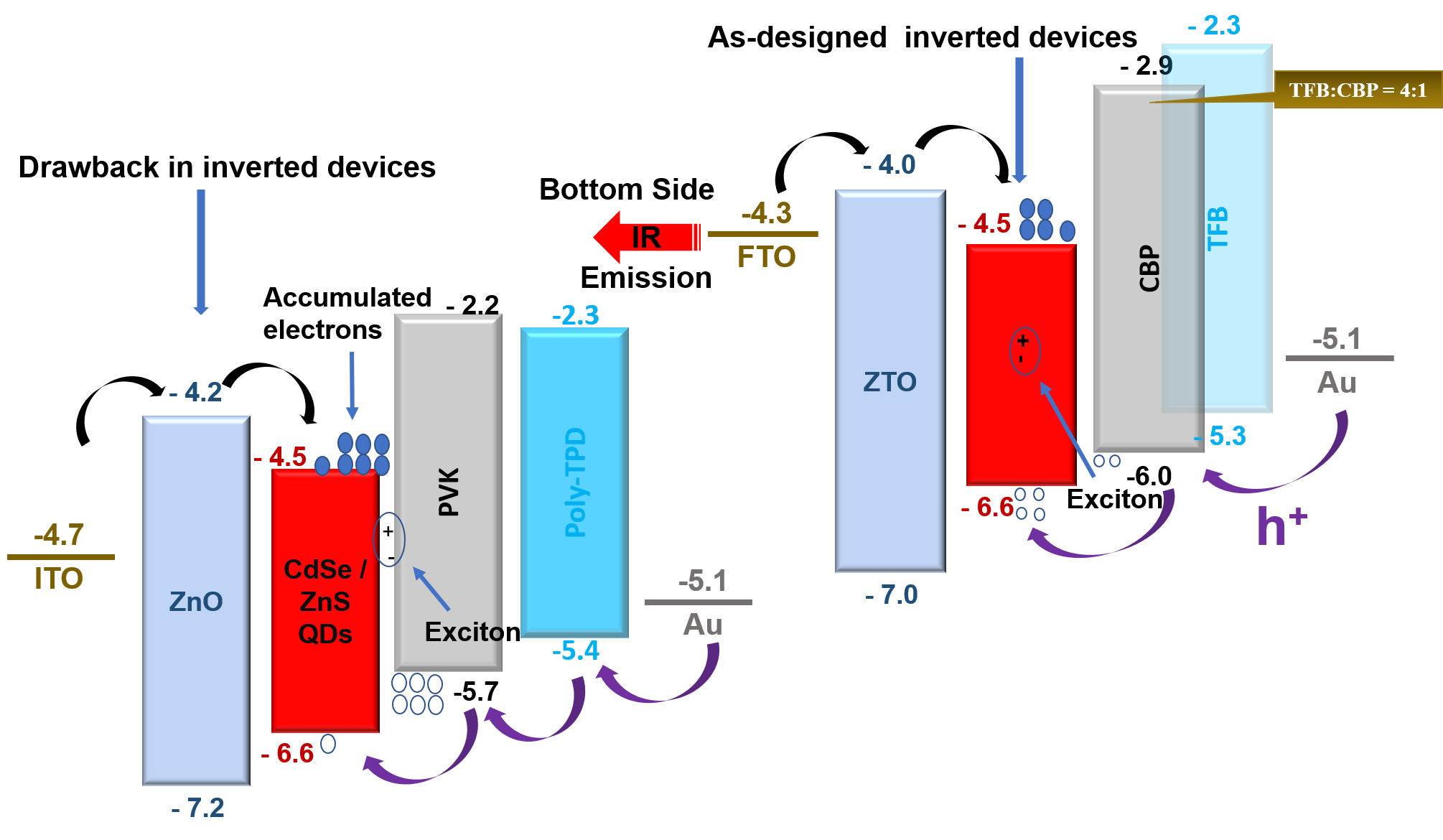
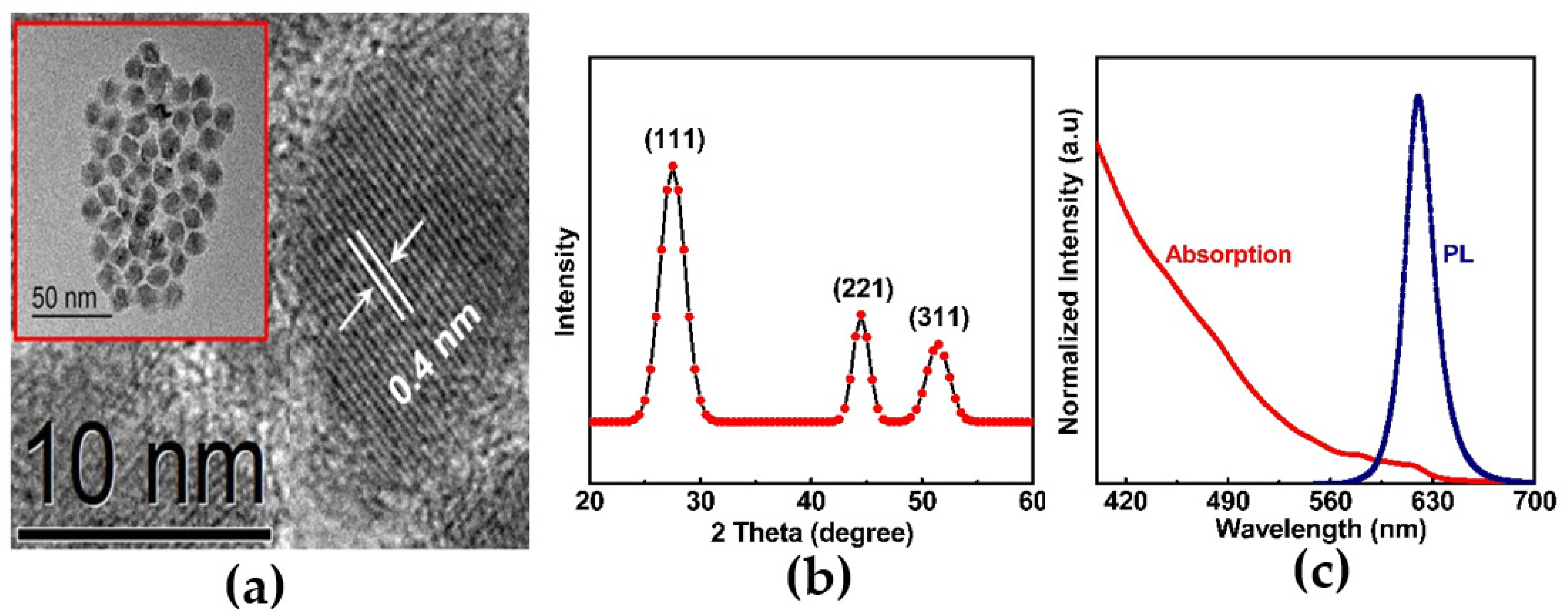
3. Results and Discussion

Figure 1a (inset), represents high-resolution transmission electron microscopy (HRTEM) and TEM images of CdSe/ZnS QDs with a particle size of 10 nm, a spherical shape, and homogenous size distribution. Figure 1a displays a distinct lattice structure with a d-spacing of 0.4 nm, which is consistent with the literature and indicates strong crystallinity in the synthesized QDs [38]. The X-ray diffraction (XRD) pattern in Figure 1b indicates that the diffraction peaks (111), (221), and (311) belong to the cubic phase of the synthesized CdSe/ZnS QDs [39]. The UV-vis-absorption and PL spectra of the fabricated QDs (in solution) are shown in Figure 1c. The absorption and luminescence peaks of quantum dots are monitored at 630 nm and 620 nm, corresponding to red light emission. The full width at half peak (FWHM) is 30 nm, and the calculated PLYQ of QDs dots (in solution) is 80% and 31% (film state), respectively.
Roughness and morphology strongly affect the suitable interface contact and efficient charge flow through the interfaces. Atomic force microscopy (AFM) height images of ZTO films on plane ITO substrate were taken and shown in Figure 2a (Figure 2b showed a three-dimensional surface topography image). The prepared ZTO film represents roughness on route mean square (RMS) 7.01 nm at 180 °C. The small RMS value of ZTO (film state) can describe the tiny grain size and flatter surface, which could passivate the surface defects, reduce the contact resistance, and improve the morphology of active layers. All of the above can be defined as reducing the fabricated device’s leakage current and principal for better device performance. The XRD patterns are also illustrated of ZTO film in Figure 2c. Only one peak showed on the ZTO phase, indicating that the fabricated ETL has an amorphous rather than crystalline structure. However, XRD exhibits a single peak at 32.5°, which means that precursors slightly impact the ZTO film’s crystallinity in preparation conditions because the preparation method can control crystallinity. Therefore, the ZTO film shows an amorphous structure [40].
The surface morphology of the ZTO with different layers is examined on plane ITO taken by SEM as shown in Figure 3a,b. A single layer of ZTO shows huge pinholes that cause the leakage current and increase the structure’s heat, affecting the performance of the entire layers’ interfaces. To overcome these issues, two layers of ZTO exhibit pinhole-free surface, which improved the performance of the QD-LED.
The inverted QD-LED with hybrid HTL and solution-processed ETL was fabricated, as shown in Figure 4a,b using the following structure; FTO/ZTO (45 nm)/CdSe-ZnS (40 nm)/TFB:CBP (50 nm)/Au (100 nm). To better charge insertion into EML, increase stability, and understand the working principle, composite HTL, and ZTO ETL were used. With an electron affinity of 4.0 eV and an ionization potential of ~7.2 eV, the ZTO layer allows more efficient electron transport from the FTO into QD, which acts to limit holes inside QD owing to their valance band offset at QD/ZTO interfaces, resulting in excellent charge recombination. Zn-Sn-O (ZTO) is kind of an n-type oxide material that combines ZnO and SnO2. Alternatively, composite HTL due to deep valance band, high hole mobility, and complex structure helps electron injection into QD. We fabricated an inverted QD-LED for a reference device with the following structure; ITO/ZnO/CdSe-ZnS/PVK/Poly-TPD/Au.
The current density–voltage (J–V) characteristics of the QD-LED are shown in Figure 5a. QD-LED inverted structure with good efficiency was obtained with ZTO based ETL of the designed device as compared to the reference device. Reduced J of QD-LED devices through ZTO indicates better charge carrier injection from the ETL to the CdSe/ZnS QDs. Figure 5b demonstrates that the ZTO-based LED has a slightly higher luminance than that of the LED with the reference device. In reference and as-designed devices, the turn-on voltage VT (1 cd m−2) is 2.4 V and 1.9 V, respectively, which proves an efficient injection and balanced structure in ZTO-based QD-LED. The maximum brightness of the inverted structure device is 4296 CD m−2 at 5 V (ZTO ETL) and 3146 CD m−2 at 7.5 V (ZnO ETL). A 1.7-factor enhancement in luminance was demonstrated due to the charge-balanced structure and stability of the designed inverted QD-LED. The as-designed device showed a significant increase in external quantum efficiency (EQE), as illustrated in Figure 5c. For inverted QD-LED devices, the EQE with ZTO and ZnO is 3.97% and 2.91%, respectively. The improvement in EQE ZTO-based QD-LED indicates the minimized leakage current. An incredible enhancement in current efficiency (CE) of 7.36 cd A−1 is found, as shown in Figure 5d, which is indicated to improve the charge balance and affect the device’s performance. The performance of QD-LEDs as designed and reference devices is summarized in Table 1.
To confirm the effect of the carrier injection on charge transport, hybrid hole-only devices (HOD) and electron-only devices (EOD) were fabricated, and their J-V characteristics were measured as shown in Figure 6a They show well-balanced charge injection into QDs and equally, electron–hole recombination occurs and improves device performance. Without any encapsulation, the device’s stability was optimized in natural conditions at 60% humidity.
The PL of the QD (in film state) and the EL of the as-designed device are compared in Figure 6b. Because of the Stark effect and/or the Forster resonance energy transfer, the PL peak is blue-shifted from the EL peak.

4. Conclusions

In summary, we used CdSe/ZnS QDs to build inverted QD-LED devices with ZTO ETL and hybrid HTL. A composite layer of TFB polymer and the small molecule CBP was shown to be an excellent HTL for producing brilliant and efficient QD-LEDs. Taking advantage of TFB’s high mobility and deep-seated HOMO CBP level, TFB:CBP composite HTL may increase hole handling ability and reduce the energy barrier for injecting holes into the device. The L-V analysis confirms that LED with ZTO ETL demonstrates a 1.7-fold improvement compared to the reference LED. The QD-LED device with ZTO ETL showed a good luminance of 4296 cd m−2, a current efficiency of 7.36 cd A−1, and an EQE of 3.97%. The proposed inverted QD-LED has a lower turn-on voltage (Vt) than the reference device, owing to better energy level matching and carrier injection into the QD emission layer. As a result, QD-LED devices will show benefits and new opportunities for optoelectronic devices such as photodetectors, field-effect transistors, and solar cells. In addition, the thorough investigation expands the potential for improving device stability and efficiency in real-world applications.

Author Contributions

Conceptualization, S.H. and W.L.; Data curation, S.H., F.S., Q.K. and W.L.; Formal analysis, S.H., F.S., A.P., A.A., N.D., Z.C., J.C., Q.K. and W.L.; Investigation, A.R. and J.C.; Methodology, S.H., A.R. and Q.K.; Visualization, S.H.; Writing—original draft, S.H. All authors have read and agreed to the published version of the manuscript.

Funding

This work is financially supported by the funding of the National Key Research and Development Program of China (2018YFE0125500, 2016YFB0401600).

Data Availability Statement

All data generated or analyzed during this study are included in this published article.

Acknowledgments

This work is financially supported by the funding of the National Key Research and Development Program of China (2018YFE0125500, 2016YFB0401600), Program 111_2.0 in China (BP0719013), National Natural Science Foundation Project of China (61775034, 51879042, 61674029, 12005038), Research Fund for International Young Scientists (62050410350), an international cooperative research project of Jiangsu province (BZ2018056), Leading Technology of Jiangsu Basic Research Plan (BK20192003), the Aeronautical Science Foundation of China (201951069001), and Jiangsu province college graduate research innovation program (KYLX16_0213).

Conflicts of Interest

The authors declare no competing financial interest.

References

  1. Khan, Q.; Subramanian, A.; Yu, G.; Maaz, K.; Li, D.; Sagar, R.U.R.; Chen, K.; Lei, W.; Shabbir, B.; Zhang, Y. Structure optimization of perovskite quantum dot light-emitting diodes. Nanoscale 2019, 11, 5021–5029. [Google Scholar] [CrossRef]
  2. Zhang, H.; Chen, S. An ZnMgO:PVP inorganic-organic hybrid electron transport layer: Towards efficient bottom-emission and transparent quantum dot light-emitting diodes. J. Mater. Chem. C 2019, 7, 2291–2298. [Google Scholar] [CrossRef]
  3. Lee, M.H.; Chen, L.; Li, N.; Zhu, F. MoO3-induced oxidation doping of PEDOT:PSS for high performance full-solution-processed inverted quantum-dot light emitting diodes. J. Mater. Chem. C 2017, 5, 10555–10561. [Google Scholar] [CrossRef] [Green Version]
  4. Mashford, B.S.; Stevenson, M.; Popovic, Z.; Hamilton, C.; Zhou, Z.; Breen, C.; Steckel, J.; Bulovic, V.; Bawendi, M.; Coe-Sullivan, S.; et al. High-efficiency quantum-dot light-emitting devices with enhanced charge injection. Nat. Photonics 2013, 7, 407–412. [Google Scholar] [CrossRef]
  5. Coe, S.; Woo, W.K.; Bawendi, M.; Bulović, V. Electroluminescence from single monolayers of nanocrystals in molecular organic devices. Nature 2002, 420, 800–803. [Google Scholar] [CrossRef]
  6. Zhao, J.; Bardecker, J.A.; Munro, A.M.; Liu, M.S.; Niu, Y.; Ding, I.K.; Luo, J.; Chen, B.; Jen, A.K.Y.; Ginger, D.S. Efficient CdSe/CdS quantum dot light-emitting diodes using a thermally polymerized hole transport layer. Nano Lett. 2006, 6, 463–467. [Google Scholar] [CrossRef] [PubMed]
  7. Caruge, J.M.; Halpert, J.E.; Wood, V.; Buloví, V.; Bawendi, M.G. Colloidal quantum-dot light-emitting diodes with metal-oxide charge transport layers. Nat. Photonics 2008, 2, 247–250. [Google Scholar] [CrossRef]
  8. Cho, K.S.; Lee, E.K.; Joo, W.J.; Jang, E.; Kim, T.H.; Lee, S.J.; Kwon, S.J.; Han, J.Y.; Kim, B.K.; Choi, B.L.; et al. High-performance crosslinked colloidal quantum-dot light-emitting diodes. Nat. Photonics 2009, 3, 341–345. [Google Scholar] [CrossRef]
  9. Qian, L.; Zheng, Y.; Xue, J.; Holloway, P.H. Stable and efficient quantum-dot light-emitting diodes based on solution-processed multilayer structures. Nat. Photonics 2011, 5, 543–548. [Google Scholar] [CrossRef]
  10. Kwak, J.; Bae, W.K.; Lee, D.; Park, I.; Lim, J.; Park, M.; Cho, H.; Woo, H.; Yoon, D.Y.; Char, K.; et al. Bright and efficient full-color colloidal quantum dot light-emitting diodes using an inverted device structure. Nano Lett. 2012, 12, 2362–2366. [Google Scholar] [CrossRef]
  11. Bae, W.K.; Park, Y.S.; Lim, J.; Lee, D.; Padilha, L.A.; McDaniel, H.; Robel, I.; Lee, C.; Pietryga, J.M.; Klimov, V.I. Controlling the influence of Auger recombination on the performance of quantum-dot light-emitting diodes. Nat. Commun. 2013, 4, 3661. [Google Scholar] [CrossRef] [Green Version]
  12. Qasim, K.; Wang, B.; Zhang, Y.; Li, P.; Wang, Y.; Li, S.; Lee, S.T.; Liao, L.S.; Lei, W.; Bao, Q. Solution-Processed Extremely Efficient Multicolor Perovskite Light-Emitting Diodes Utilizing Doped Electron Transport Layer. Adv. Funct. Mater. 2017, 27, 1606874. [Google Scholar] [CrossRef]
  13. Subramanian, A.; Pan, Z.; Zhang, Z.; Ahmad, I.; Chen, J.; Liu, M.; Cheng, S.; Xu, Y.; Wu, J.; Lei, W.; et al. Interfacial Energy-Level Alignment for High-Performance All-Inorganic Perovskite CsPbBr3 Quantum Dot-Based Inverted Light-Emitting Diodes. ACS Appl. Mater. Interfaces 2018, 10, 13236–13243. [Google Scholar] [CrossRef] [PubMed]
  14. Dai, X.; Zhang, Z.; Jin, Y.; Niu, Y.; Cao, H.; Liang, X.; Chen, L.; Wang, J.; Peng, X. Solution-processed, high-performance light-emitting diodes based on quantum dots. Nature 2014, 515, 96–99. [Google Scholar] [CrossRef] [PubMed]
  15. Son, D.I.; Kim, H.H.; Cho, S.; Hwang, D.K.; Seo, J.W.; Choi, W.K. Carrier transport of inverted quantum dot LED with PEIE polymer. Org. Electron. 2014, 15, 886–892. [Google Scholar] [CrossRef]
  16. Liu, B.; Lan, L.; Liu, Y.; Tao, H.; Li, H.; Xu, H.; Zou, J.; Xu, M.; Wang, L.; Peng, J.; et al. Improved performance of quantum dot light-emitting diodes by hybrid electron transport layer comprised of ZnO nanoparticles doped organic small molecule. Org. Electron. Phys. Mater. Appl. 2019, 74, 144–151. [Google Scholar] [CrossRef]
  17. Subramanian, A.; Akram, J.; Hussain, S.; Chen, J.; Qasim, K.; Zhang, W.; Lei, W. High-Performance Photodetector Based on a Graphene Quantum Dot/CH 3 NH 3 PbI 3 Perovskite Hybrid. ACS Appl. Electron. Mater. 2020, 2, 230–237. [Google Scholar] [CrossRef]
  18. Hussain, S.; Raza, A.; Saeed, F.; Perveen, A.; Sikhai, Y.; Din, N.; Elemike, E.E. Stable and high performance all-inorganic perovskite light-emitting diodes with anti-solvent treatment. Chin. Opt. Lett. 2021, 19, 030005. [Google Scholar] [CrossRef]
  19. Kim, D.J.; Lee, H.N. Improving the charge balance and performance of CdSe/ZnS quantum-dot light-emitting diodes with a sputtered zinc-tin-oxide electron-transport layer and a thermally evaporated tungsten-oxide charge-restricting layer. Jpn. J. Appl. Phys. 2019, 58, 106502. [Google Scholar] [CrossRef]
  20. Kim, T.G.; Shin, D.S.; Jung, K.Y.; Kadam, A.N.; Park, J. Improving light extraction in light-emitting diodes using zinc-tin-oxide layers. J. Alloys Compd. 2017, 710, 399–402. [Google Scholar] [CrossRef]
  21. Park, M.; Roh, J.; Lim, J.; Lee, H.; Lee, D. Double metal oxide electron transport layers for colloidal quantum dot light-emitting diodes. Nanomaterials 2020, 10, 726. [Google Scholar] [CrossRef] [Green Version]
  22. Joo, Y.H.; Wi, J.H.; Lee, W.J.; Chung, Y.D.; Cho, D.H.; Kang, S.; Um, D.S.; Kim, C. Il Work function tuning of zinc–tin oxide thin films using high-density o2 plasma treatment. Coatings 2020, 10, 1026. [Google Scholar] [CrossRef]
  23. Ji, W.; Tian, Y.; Zeng, Q.; Qu, S.; Zhang, L.; Jing, P.; Wang, J.; Zhao, J. Efficient quantum dot light-emitting diodes by controlling the carrier accumulation and exciton formation. ACS Appl. Mater. Interfaces 2014, 6, 14001–14007. [Google Scholar] [CrossRef]
  24. Cho, Y.R.; Kang, P.; Shin, D.H.; Kim, J.; Maeng, M.; Sakong, J.; Hong, J.; Park, Y.; Suh, M.C. Effect of anode buffer layer on the efficiency of inverted quantum-dot light-emitting diodes. Appl. Phys. Express 2015, 9, 012103. [Google Scholar] [CrossRef]
  25. Lin, W.; Wu, J.L.; Zhang, Q.M.; Lei, Y.L.; Chen, L.X. High-performance full-solution-processed quantum dot lightemitting diodes with a doped hole injection layer. Sci. Sin. Phys. Mech. Astron. 2020, 50, 067301. [Google Scholar] [CrossRef]
  26. Choi, M.K.; Yang, J.; Kim, D.C.; Dai, Z.; Kim, J.; Seung, H.; Kale, V.S.; Sung, S.J.; Park, C.R.; Lu, N.; et al. Extremely Vivid, Highly Transparent, and Ultrathin Quantum Dot Light-Emitting Diodes. Adv. Mater. 2017, 30, 1703279. [Google Scholar] [CrossRef]
  27. Sun, Y.; Su, Q.; Zhang, H.; Wang, F.; Zhang, S.; Chen, S. Investigation on Thermally Induced Efficiency Roll-Off: Toward Efficient and Ultrabright Quantum-Dot Light-Emitting Diodes. ACS Nano 2019, 13, 11433–11442. [Google Scholar] [CrossRef] [PubMed]
  28. Ding, K.; Fang, Y.; Dong, S.; Chen, H.; Luo, B.; Jiang, K.; Gu, H.; Fan, L.; Liu, S.; Hu, B.; et al. 24.1% External Quantum Efficiency of Flexible Quantum Dot Light-Emitting Diodes by Light Extraction of Silver Nanowire Transparent Electrodes. Adv. Opt. Mater. 2018, 6, 1800347. [Google Scholar] [CrossRef]
  29. Fang, Y.; Ding, K.; Wu, Z.; Chen, H.; Li, W.; Zhao, S.; Zhang, Y.; Wang, L.; Zhou, J.; Hu, B. Architectural Engineering of Nanowire Network Fine Pattern for 30 μm Wide Flexible Quantum Dot Light-Emitting Diode Application. ACS Nano 2016, 10, 10023–10030. [Google Scholar] [CrossRef] [PubMed]
  30. Son, D.I.; Kim, H.H.; Hwang, D.K.; Kwon, S.; Choi, W.K. Inverted CdSe-ZnS quantum dots light-emitting diode using low-work function organic material polyethylenimine ethoxylated. J. Mater. Chem. C 2014, 2, 510–514. [Google Scholar] [CrossRef]
  31. Zhao, Y.; Chen, L.; Wu, J.; Tan, X.; Xiong, Z.; Lei, Y. Composite Hole Transport Layer Consisting of High-Mobility Polymer and Small Molecule with Deep-Lying HOMO Level for Efficient Quantum Dot Light-Emitting Diodes. IEEE Electron Device Lett. 2020, 41, 80–83. [Google Scholar] [CrossRef]
  32. Khan, Q.; Subramanian, A.; Ahmed, I.; Khan, M.; Nathan, A.; Wang, G.; Wei, L.; Chen, J.; Zhang, Y.; Bao, Q. Overcoming the Electroluminescence Efficiency Limitations in Quantum-Dot Light-Emitting Diodes. Adv. Opt. Mater. 2019, 7, 1900695. [Google Scholar] [CrossRef]
  33. Hussain, S.; Subramanian, A.; Yan, S.; Din, N.; Abbas, G.; Shuja, A.; Lei, W.; Khan, Q. Engineering Architecture of Quantum Dot-Based Light-Emitting Diode for High Device Performance with Double-Sided Emission Fabricated by Nonvacuum Technique. ACS Appl. Electron. Mater. 2020, 2, 2383–2389. [Google Scholar] [CrossRef]
  34. Li, Y.; He, P.; Chen, S.; Lan, L.; Dai, X.; Peng, J. Inkjet-Printed Oxide Thin-Film Transistors Based on Nanopore-Free Aqueous-Processed Dielectric for Active-Matrix Quantum-Dot Light-Emitting Diode Displays. ACS Appl. Mater. Interfaces 2019, 11, 28052–28059. [Google Scholar] [CrossRef]
  35. Zhang, X.; Li, Q.; Yan, S.; Lei, W.; Chen, J.; Khan, Q. A Novel Phototransistor Device with Dual Active layers composited of CsPbBr3 and ZnO Quantum Dots. Materials 2019, 12, 1215. [Google Scholar] [CrossRef] [PubMed] [Green Version]
  36. Beek, W.J.E.; Wienk, M.M.; Kemerink, M.; Yang, X.; Janssen, R.A.J. Hybrid zinc oxide conjugated polymer bulk heterojunction solar cells. J. Phys. Chem. B 2005, 109, 9505–9516. [Google Scholar] [CrossRef]
  37. Zhang, Q.; Xia, G.; Li, L.; Xia, W.; Gong, H.; Wang, S. High-performance Zinc-Tin-Oxide thin film transistors based on environment friendly solution process. Curr. Appl. Phys. 2019, 19, 174–181. [Google Scholar] [CrossRef]
  38. Mustafa, M.; Zubair, M.; Mustafa, M.; Lee, K.; Yoon, C.; Hoi, Y. Fabrication of CdSe/ZnS quantum dots thin film by electrohydrodynamics atomization technique for solution based flexible hybrid OLED application Fabrication of CdSe/ZnS quantum dots thin film by electrohydrodynamics atomization technique for solution. Chem. Eng. J. 2014, 253, 325–331. [Google Scholar] [CrossRef]
  39. Chang, Y.; Sun, D.; Zhang, Z.; Zhang, Y.; Yao, X.; Jiang, D.; Yu, Y.; Mi, L.; Chen, L.; Zhong, H.; et al. High color-rendering-index Hybrid white LEDs employing CdSe/ZnS core/shell quantum dots. J. Nanosci. Nanotechnol. 2016, 16, 670–676. [Google Scholar] [CrossRef]
  40. Zhao, Y.; Dong, G.; Duan, L.; Qiao, J.; Zhang, D.; Wang, L.; Qiu, Y. Impacts of Sn precursors on solution-processed amorphous zinc-tin oxide films and their transistors. RSC Adv. 2012, 2, 5307–5313. [Google Scholar] [CrossRef]
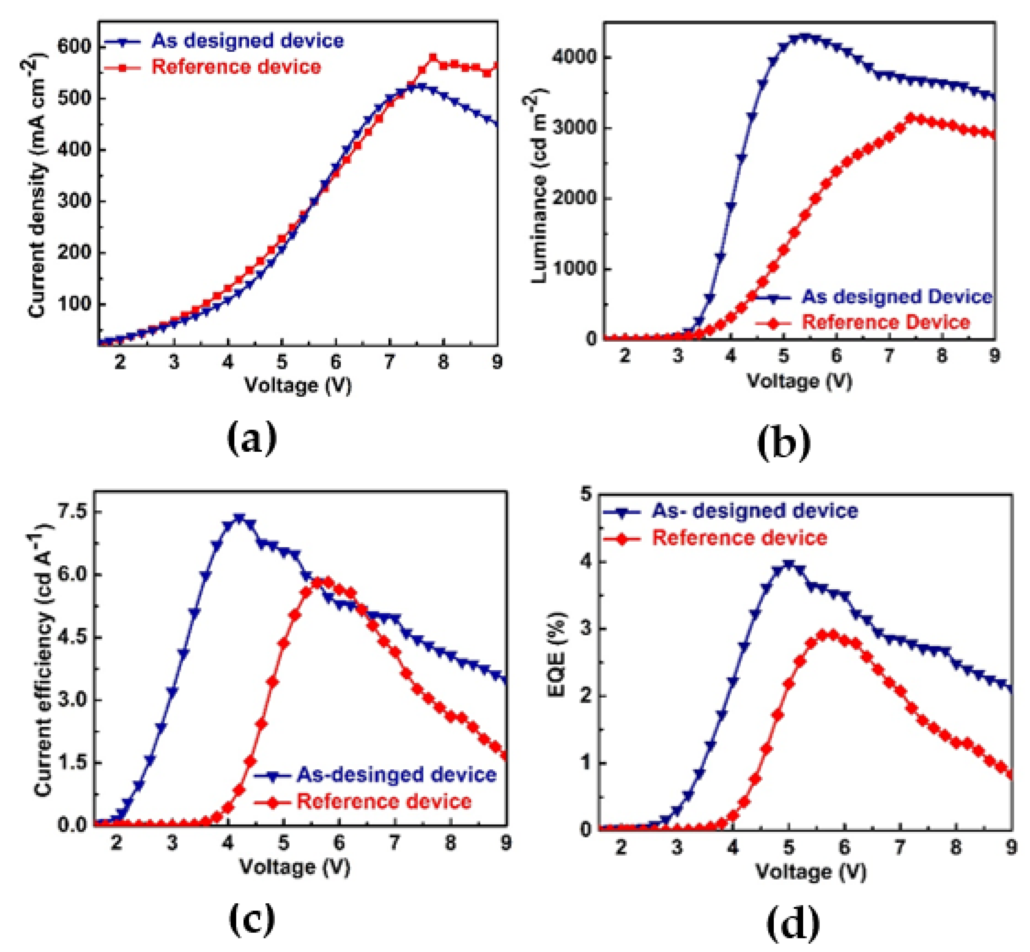
Figure 1. Characteristics of CdSe/ZnS core–shell QDs; (a) HRTEM and TEM images; (b) XRD pattern; and (c) UV−vis absorption and PL spectra.
Electronics 10 02290 g001
Figure 2. ZTO Characteristics (a) AFM height image; (b) 3D images; (c) XRD pattern.
Electronics 10 02290 g002
Figure 3. Scanning Electron microscopy (SEM) images; (a) one layer of ZTO; (b) two layers of ZTO.
Electronics 10 02290 g003
Figure 4. (a) Energy-level diagram of QD-based LED; (b) Schematic presentation of the fabrication of QD-LED.
Electronics 10 02290 g004
Figure 5. Comparisons results; (a) current density vs. voltage (V); (b) luminance vs. V; (c) current efficiency vs. V; (d) external quantum efficiency vs. V.
Electronics 10 02290 g005
Figure 6. (a) HODs and EODs comparisons; (b) comparison of the EL spectrum of an as-designed device with the PL spectrum of the QDs in film state.
Electronics 10 02290 g006
Table 1. Comparisons of the characteristics of the reference device and as-designed device.
Device No.StructureVT(V) Lmax (cd m−2)EQE (%)
Reference deviceFTO/ZnO/CdSe-ZnS/PVK/Poly-TBD/Au2.431462.91
As-designed deviceFTO/ZTO/CdSe-ZnS/TFB:CBP/Au1.9 42963.97
Publisher’s Note: MDPI stays neutral with regard to jurisdictional claims in published maps and institutional affiliations.

