Visible to Mid-infrared Waveband Photodetector Based on Insulator Capped Asymmetry Black Phosphorous
 Qi Han
 Yadong Jiang1,2
 - 1School of Optoelectronic Science and Engineering, University of Electronic Science and Technology of China, Chengdu, China
- 2State Key Laboratory of Electronic Thin Films and Integrated Devices, University of Electronic Science and Technology of China, Chengdu, China
Processing layer-dependent direct band gap and good absorption coefficient especially in the mid-infrared band, black phosphorous is believed to make a contribution superior to that of graphene in broadband photodetectors. The narrow band gap of 0.3 eV for bulk black phosphorous helps to absorb infrared radiation while a relatively large dark current under zero gate voltage is inevitable. Few layer black phosphorous sheets with asymmetrical thickness sealed in an insulator for protection is designed and explored for photosensitive mechanism in this work. Saturable absorption dominates the light harvesting process in visible light detection and thus limits maximum photocurrent to 3.3 and 1.4 μA for 520 and 650 nm lasers with a dark current of 0.7 μA. While in near-infrared wavelength, a responsivity of 0.12 A/W is inducted for 808 nm free of adsorption saturation even if the incident power is increased to 200
Introduction
Black phosphorous (BP) is a two-dimensional material with a layer-dependent bandgap. Although the orthorhombic crystal group as well as some basic parameters such as lattice dimensions have been determined by Brown et al. in 1965 [1], detailed research of BP boomed after the successful exfoliation of graphene [2]. A poor absorption coefficient gets graphene over a barrel in optical detection [3]. Thus, a series of two-dimensional material including BP is investigated and made instead. The bandgap of BP monotonically decreases from 1.8 to 0.3 eV as the number of layers grows [4]. Zhang et al. confirmed the layer-dependent feature of phosphorene through photoluminescence for two to five layers BP [5]. In bulk form, BP processes a direct bandgap of 0.3 eV, especially suitable for mid-infrared light detection. Several previous works present BP’s infrared light harvesting effect, the wavelength ranging from 1.5 to 7.7 μm [6–10]. A silicon-compatible photovoltaic BP photodetector is made by Youngblood et al. and demonstrates fast response and low dark current [6]. Deng constructs a van der Waals heterojunction of black phosphorous and
In this work, asymmetric BP is fabricated and serves as a photodetector. Saturable absorption effect is observed in the visible waveband. That is, the amplitude of the photocurrent fails to grow if the incident radiation power is increased to a certain plateau. Besides, these plateaus diverge for different wavelengths. The pinning effect shaped the IV curve of asymmetric BP. An uneven quasi Fermi level accounts for the observed apparent and fast response in visible and near-infrared waveband. A modeling of a BP sheet by use of technology computer aided design (TCAD) shows distinct line shapes of symmetric and asymmetric conditions, confirming the theory of uneven p doping of asymmetric BP. Moderate responsivity (several hundred milli-amperes per watt) and relatively fast response (∼200 μs) is acquired for visible light. More details of the energy band as well as bias dependent photocurrent can be provided by simulation. Then, the photo-response in the mid-infrared band is measured. The response is believed to originate in the heat transition process, observed from a negative photocurrent independent of sheet uniformity. The photosensitive mechanism for mid-infrared is contrary to visible and near-infrared waveband. Compared to an ordinary BP sheet, the asymmetric BP demonstrates higher responsivity and wider waveband sensitivity.
Materials and Methods
Au electrodes are deposited on 300 nm SiO2/Si substrate with a 10-nm chromium moist layer, followed by BP transferring by use of the universal two-dimensional material dry transfer method [18, 19]. Electric features measurement is carried on bare BP. The BP bulk material is purchased from Nanjing MuKe Nanotechnology Co., Ltd. Then, a layer of exfoliated h-BN, purchased from Six-Carbon Technology (Shenzhen, China), is also transferred, covering the BP. The photocurrent is collected by a PDA source meter. A narrow band filter centered at 3.5 or 4.5 μm with a full width at half maximum of 500 nm is placed before a black body for certain mid-infrared wavelengths. The spot size for these mid-infrared filtered lights is estimated as
Results and Discussion
A pair of obtuse angle gold electrodes is prepared by lithography and patterning of electrodes, and then an asymmetric, bare BP sheet is transferred on an SiO2/Si substrate, as illustrated in Figure 1A. Uneven thickness is clearly observed from the different color in the upper part of the inset. As previous research shows, thickness of the BP varies with the color under an optical microscope and shows weak periodic feature. This holds for both epitaxial of high-crystalline and exfoliated BP condition [13, 20]. To apply the method to asymmetric BP, various types of setups of BP and metal electrodes are evaluated by profilometer and metallographic microscope; see supplement information.
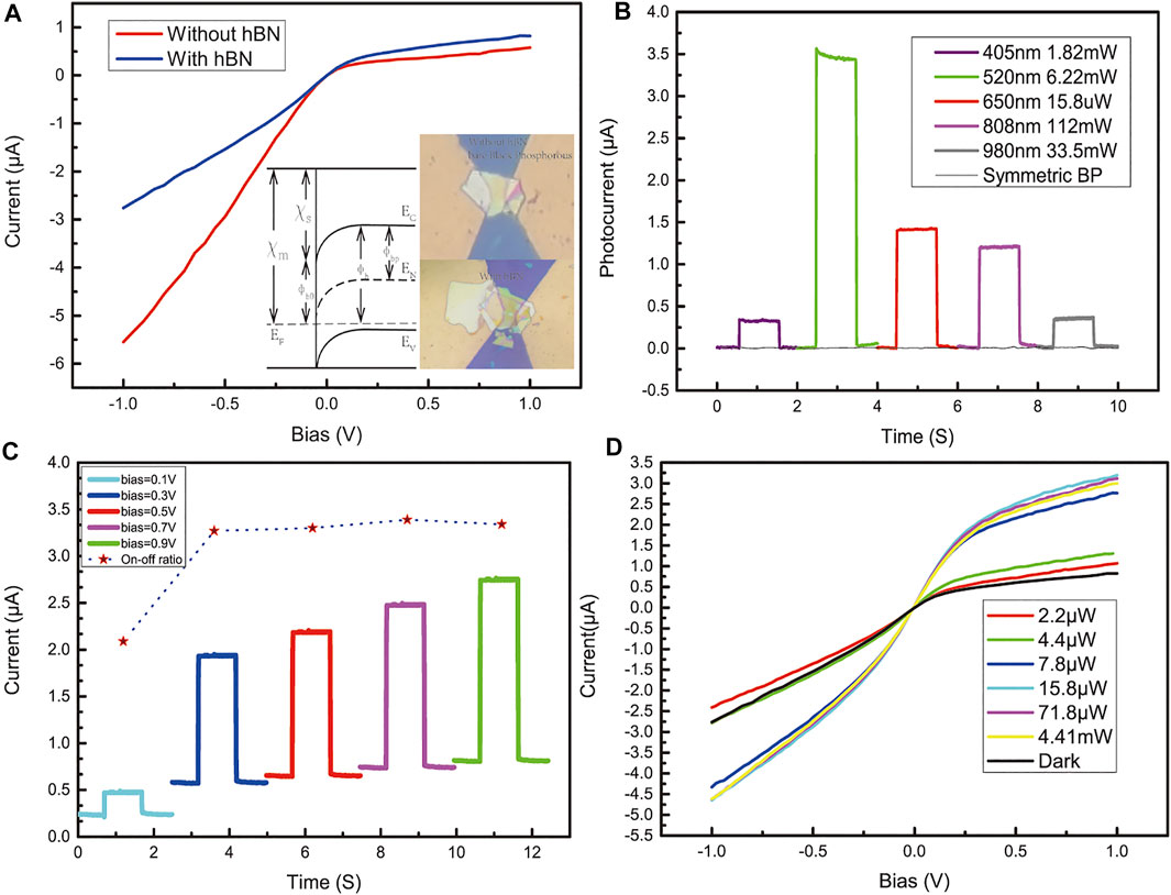
FIGURE 1. Electrical feature and photocurrent of asymmetric BP. (A) Voltage-ampere characteristic curve of symmetric and asymmetric BP. (B) Saturable absorption photocurrent of asymmetric BP for various wavelengths in the visible waveband. (C) On-off and photocurrent of asymmetric BP with different bias voltage. (C) Voltage-ampere characteristic curve of asymmetric BP under a 650-nm laser with increasing power.
A typical Schottky barrier in a junction of metal and BP is
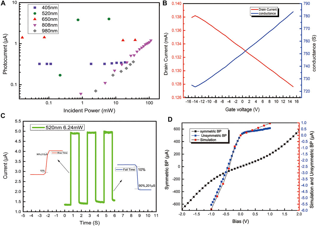
FIGURE 2. Saturation absorption and simulation parameter extraction of asymmetric BP. (A) Photocurrent as a function of incident power for a wide waveband from 405 to 980 nm. In the visible waveband, a maximum photocurrent is observed, and saturable absorption feature is clear. (B) Transfer characteristic curve of a symmetric bulk BP sheet. (C) Response time of asymmetric BP under a 520-nm laser. (D) Voltage-ampere characteristic curve of simulation and experiment results of BP.
For our asymmetric BP, the situation is different. The IV curve shows an abrupt change of slope around zero bias in Figure 1A. Curvature tends to be gigantic in both the positive and negative bias voltage range. Besides, the rectifying ratio reaches 9.2, see IV curve without hexagonal boron nitride (h-BN). It is the red line in Figure 1A for bare BP. This behavior of the IV curve is different from ohm-contact BP field-effect transistors [21], a heterojunction formed by BP and another semiconductor [22, 23] or a Schottky connection formed from a connection of a semiconductor and metal.
To explain this unique electric, a dipole formed by pinning effect is introduced. At the interface of metal and semiconductor contact, there is an always finite density of states called metal-induced gap states (MIGS) with complex wave vector. The abrupt change of geometry results in an energy level splitting at the interface. As a result, the metal allows states at all energies [24]. Sometimes its influence cannot be ignored. These metal-induced gap states give a dipole
When we take a closer look at the IV curve of asymmetric BP, there is a combination of ohmic contact and Schottky contact. In a very little range of bias voltage around zero, there is still a curvature in the IV curve, meaning an inevitable barrier is present. In the process of forming the ohmic contact, electrons in metal can move fluently in BP and thus deduce BP’s original p doping and uplift the quasi Fermi level for holes. Finally, more metal-induced gap states are occupied, and the intrinsic doping is decreased. As a result, a more balanced IV curve is observed.
BP lacks water, oxygen, and light stability [14]. The existing strategy to make better stability includes covalent functionalization [25] and additional material capping [15]. In this work, to decrease the degradation of BP, a layer of h-BN is exfoliated and transferred onto the BP, as shown in the bottom part of the inset of Figure 1A. The line shape of volt-ampere characteristics stays the same, while the amount of slope rate unignorably decreases. The rectifying ratio declines to 3.2, implying the barrier of the junction is attenuated by the h-BN capping. In the pinning diagram, the dipole as well as the pinning strength relies on the gap in the junction. The gap is varied in the process of h-BN transferred due to additional force and weight and it may be the reason of the change in IV curve after the transferring of the h-BN. In the process of preparing the device, to liberate the sample from PDMS to the substrate, the holder for the sample should be heated. BP requires less than 40°C to be released, and h-BN usually requires 75°C. The press and the heat may strengthen the connection of BP and the metal. The influence of dielectric layers to the doping type and level is also reported by Nathan et al. [6], but it is not applicable in the asymmetric BP here, for the absolute value changes in different ways for positive and negative bias. Although encapsulated, the device may be degraded 1 mo later, and the speed of degradation can be accelerated by illumination to our experience.
Due to this asymmetric characteristic, optical electronic performance is also enhanced for visible and near-infrared wavelengths. Compared to a uniform BP sheet, an asymmetric device provides larger photocurrent in visible and near-infrared wavelength, as shown in Figure 1B. Little photocurrent can be acquired for an ordinary symmetric BP. The optical sensitive feature is distinct from many traditional materials, such as silicon due to its small and direct band gap (∼0.3 eV). For a photon with energy much larger than the band gap but not enough to induce an Auger effect, there is still only one pair of photo-excited carriers. Excess energy is turned into kinetic energy of electrons and phonons. Therefore, when a photodetector made of BP works at the visible waveband, photo energy leakage is inevitable. As a result, the absorption coefficient of bulk BP to photons between 0.3 and 3 eV is relatively poor [26]. The saturable absorption phenomena is also recorded for BP quantum dots for ultrafast photonics [27]. In Figure 1B, the least energy eligible for saturable absorption is applied on the asymmetric BP and corresponding photocurrent is plotted. No monotonous law is found in the relationship between max photocurrent and least saturable absorption energy. However, larger energy can be more acceptable for longer wavelengths. The measurement is limited by max power the lasers can provide in the 808 and 980 nm cases.
Gate voltage is usually needed for ordinary BP photodetectors to achieve reasonable on-off ratio. Varying the gate voltage frequently in analog devices may require additional preparing time and accuracy in practical application. In this experiment, the gate voltage is invariant. As illustrated by Figure 1C, asymmetric BP can reach an on-off ratio from 2.05 to 3.3 with the bias ranging from 0.1 to 0.9 V. The photo current grows proportionately with dark current when the bias is higher than 0.3 V. The photocurrent bias dependency reminds us that saturable photocurrent can be enhanced by a stronger directional electric field.
The saturation of photocurrent can be as soon as the power of incident light is increased; seeFigure 1D for details of a 650 nm case. The overall current reaches 3.04 μA under an incident power of 15.8 μW. In addition, the current slightly decreases when a higher laser power of 71.8 μW or 4.41 mW is applied. The photocurrent is opposite for a low power of 2.2 μW. This is counterintuitive. The incident light may set the device in a small signal mode. The dipole induced by the pinning effect changes its sign for reversed bias.
A comprehensive relationship of photocurrent and incident power is shown in Figure 2A. The sequence of wavelength of minimum cut off saturation power is 15.8 μW, 1.82, and 6.22 mW for 650, 405, and 520 nm. Among these, the minimum saturable energy of 405 and 650 nm is limited by the least power the laser can provide. The slope of linear fit of the photocurrent and incident power is zero if the device works at the saturable state. The responsivity is evaluated as 0.12 μA/W for an 808-nm laser. The responsivity of the device is inferior to typical commercial photodetectors, but there is a large improvement to a symmetric BP sheet. Apart from responsivity, another important parameter of photodetectors is its speed. The rising and falling time of the device is relatively short for 212 and 201 μS, respectively, seeFigure 2C. The fast rehabilitation of the photo response indicates enough shallow energy traps in the BP sheet, according to the theory of the Hornbeck−Haynes model [10, 28].
To analyze the carriers and verify our model, especially the dipole introduced by pinning effect, a simulation by means of TCAD is conducted. The transfer characteristic curve of a symmetric BP sheet is measured. The result is in Figure 2B. Hole mobility of BP is extracted following
Further information can be deduced from the simulation result, and it is helpful in the analysis of mid-infrared photo-response of BP. A dependency of photocurrent on wavelength for different band gaps is present in Figure 3A. The model for optical response is complicated and the photocurrent relies on incident power, which is set in the simulation, so the absolute value of the photocurrent is not eligible. However, relative strength of photon absorption coefficient and peak of sensitive waveband are worth noting. The band diagram of non-doped, zero biased and doped on two parts, respectively, biased BP sheets are respectively illustrated in Figures 3B,C. The carrier density can be deduced from the distance between quasi Fermi level with its conduction or valance band. There is an abrupt change of density of holes at the interface of the homogenous junction in Figure 3C. The holes accumulate more on the less doped part and a sudden decrease appears on the heavily doped part. This is intuitive due to the holes’ diffusion effect. Dependency of photocurrent on the bias voltage and band gap of BP is shown in Figure 3D. This simulation helps find an open circuit voltage and discover photo-sensitive characters of new combination sets of asymmetric BP devices.
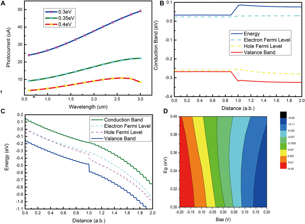
FIGURE 3. TCAD modeling result of asymmetric BP. (A) Photocurrent of asymmetric BP with different band gap. (B) The energy band diagram of undoped BP. (C) Energy diagram of p asymmetric BP with different p doping. (D) Photocurrent as a function of bias voltage and band gap of asymmetric BP.
Asymmetric BP is superior in visible and near-infrared waveband. However, in mid-infrared wavelength, a photothermic effect dominates the photocurrent. So, there is no apparent difference between asymmetric and symmetric BP in mid-infrared detection. The relationship of resistance and temperature of a symmetric BP sheet is shown in Figure 4A. As temperature increases, the resistance of BP also increases; thus, a positive temperature-resistant coefficient is observed.
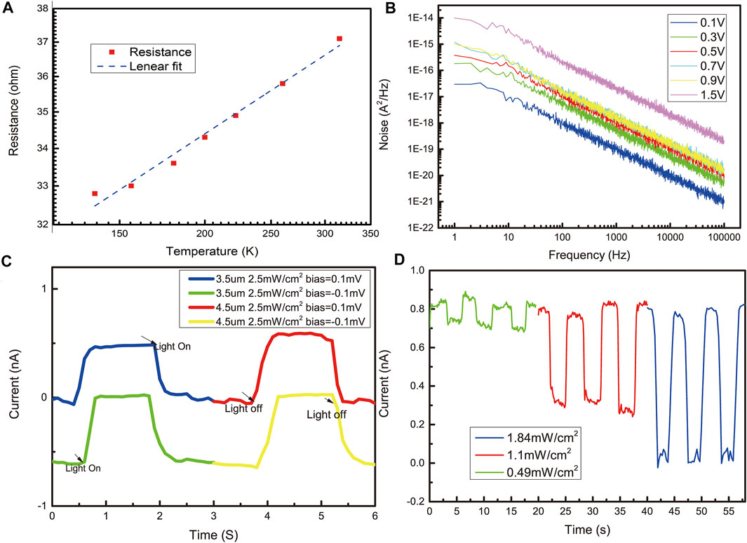
FIGURE 4. Temperature character, noise, and mid-infrared response of BP. (A) Temperature-resistant relationship of symmetric BP. (B) Noise of a typical bulk BP in mid-infrared radiation under different bias voltage. (C) Negative photocurrent of BP under mid-infrared wavelength of 3.5 and 4.5 μm. (D) Negative photocurrent of BP for different radiation power for 4.5-μm light.
A table of photodetectors associated with BPis summarized in Table 1. All the mid-infrared BP listed used a lock-in amplifier. Employing a lock-in method can filter the noise largely, so the signal to noise is greatly enhanced. A preamplifier is a recurring option combined with a lock-in amplifier. With the help of a lock-in amplifier and preamplifier, the responsivity can be enhanced. However, it is not the nature of the device. Although our device requires low bias, a time-resolved photocurrent can be observed.
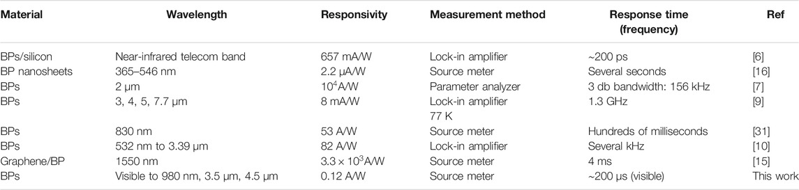
TABLE 1. A summary of black phosphorous photodetectors.
The photocurrent is negative and little in absolute value, as shown in Figure 4C for 3.5 and 4.5 μm incident power. Negative temperature-resistance coefficient of BP may account for this abnormal effect [30], though positive temperature-resistance coefficient is also reported [20]. The incident light serves as a heater and the BP sheet presents its metallicity. A dark current of ∼0.5 nA is set for the BP and the photocurrent is approximately equal in value but opposite in direction, as shown in Figure 4C. The responsivity is evaluated as 0.9 mA/W and noise equivalent power is
Conclusion
Asymmetric BP is superior in photodetection to ordinary BP in visible and near-infrared. The saturable absorption effect discovered restricts the BP’s pure photodetection practical application. However, it is still optimistic to further investigate and design certain optical devices by optimizing the parameters of asymmetric BP for its promising on-off ratio and relatively fast speed. Simulation is confirmed with the experiment in the electric feature and provides insight to developing novel appliances for BP. The temperature resistance coefficient may clarify BP’s abnormal opposite photocurrent in the mid-infrared waveband. All these experiments and analyses can pave the way for designing more outstanding broadband photodetectors based on BP.
Data Availability Statement
The original contributions presented in the study are included in the article/Supplementary Material, further inquiries can be directed to the corresponding authors.
Author Contributions
JG conceived and supervised the project. QH prepared the device and performed the photocurrent measurements and characterizations. XD and YJ set up the experimental platform, YJ and XD performed the data analysis. QH wrote this paper. All authors discussed the results and commented on the manuscript.
Funding
This work is supported by the National Natural Science Foundation of China (Grant No. 61875031) and National Natural Science Foundation-Outstanding Youth Foundation (No. 61922022).
Conflict of Interest
The authors declare that the research was conducted in the absence of any commercial or financial relationships that could be construed as a potential conflict of interest.
Publisher’s Note
All claims expressed in this article are solely those of the authors and do not necessarily represent those of their affiliated organizations, or those of the publisher, the editors and the reviewers. Any product that may be evaluated in this article, or claim that may be made by its manufacturer, is not guaranteed or endorsed by the publisher.
Supplementary Material
The Supplementary Material for this article can be found online at: https://www.frontiersin.org/articles/10.3389/fphy.2021.710150/full#supplementary-material
References
1. Brown A, Rundqvist S. Refinement of the Crystal Structure of Black Phosphorus. Acta Cryst (1965) 19:684–5. doi:10.1107/S0365110X65004140
2. Novoselov KS, Geim AK, Morozov SV, Jiang D, Zhang Y, Dubonos SV, et al. Electric Field Effect in Atomically Thin Carbon Films. Science (2004) 306:666–9. doi:10.1126/science.1102896
3. Blake P, Hill EW, Castro Neto AH, Novoselov KS, Jiang D, Yang R, et al. Making Graphene Visible. Appl Phys Lett (2007) 91:063124. doi:10.1063/1.2768624
4. Carvalho A, Wang M, Zhu X, Rodin AS, Su H, Castro Neto AH. Phosphorene: From Theory to Applications. Nat Rev Mater (2016) 1:16061. doi:10.1038/natrevmats.2016.61
5. Zhang S, Yang J, Xu R, Wang F, Li W, Ghufran M, et al. Extraordinary Photoluminescence and Strong Temperature/Angle-Dependent Raman Responses in Few-Layer Phosphorene. ACS Nano (2014) 8:9590–6. doi:10.1021/nn503893j
6. Youngblood N, Chen C, Koester SJ, Li M. Waveguide-integrated Black Phosphorus Photodetector with High Responsivity and Low Dark Current. Nat Photon (2015) 9:247–52. doi:10.1038/nphoton.2015.23
7. Huang L, Tan WC, Wang L, Dong B, Lee C, Ang K-W. Infrared Black Phosphorus Phototransistor with Tunable Responsivity and Low Noise Equivalent Power. ACS Appl Mater Inter (2017) 9:36130–6. doi:10.1021/acsami.7b09713
8. Ye L, Li H, Chen Z, Xu J. Near-Infrared Photodetector Based on MoS2/Black Phosphorus Heterojunction. ACS Photon (2016) 3:692–9. doi:10.1021/acsphotonics.6b00079
9. Chen X, Lu X, Deng B, Sinai O, Shao Y, Li C, et al. Widely Tunable Black Phosphorus Mid-infrared Photodetector. Nat Commun (2017) 8:1672. doi:10.1038/s41467-017-01978-3
10. Guo Q, Pospischil A, Bhuiyan M, Jiang H, Tian H, Farmer D, et al. Black Phosphorus Mid-infrared Photodetectors with High Gain. Nano Lett (2016) 16:4648–55. doi:10.1021/acs.nanolett.6b01977
11. Deng Y, Luo Z, Conrad NJ, Liu H, Gong Y, Najmaei S, et al. Black Phosphorus-Monolayer MoS2 van der Waals Heterojunction p-n Diode. ACS Nano (2014) 8:8292–9. doi:10.1021/nn5027388
12. Zheng S, Wu E, Feng Z, Zhang R, Xie Y, Yu Y, et al. Acoustically Enhanced Photodetection by a Black Phosphorus-MoS2 van der Waals Heterojunction p-n Diode. Nanoscale (2018) 10:10148–53. doi:10.1039/c8nr02022a
13. Xu Y, Shi X, Zhang Y, Zhang H, Zhang Q, Huang Z, et al. Epitaxial Nucleation and Lateral Growth of High-Crystalline Black Phosphorus Films on Silicon. Nat Commun (2020) 11:1330. doi:10.1038/s41467-020-14902-z
14. Huang Y, Qiao J, He K, Bliznakov S, Sutter E, Chen X, et al. Interaction of Black Phosphorus with Oxygen and Water. Chem Mater (2016) 28:8330–9. doi:10.1021/acs.chemmater.6b03592
15. Liu Y, Shivananju BN, Wang Y, Zhang Y, Yu W, Xiao S, et al. Highly Efficient and Air-Stable Infrared Photodetector Based on 2D Layered Graphene-Black Phosphorus Heterostructure. ACS Appl Mater Inter (2017) 9:36137–45. doi:10.1021/acsami.7b09889
16. Ren X, Li Z, Huang Z, Sang D, Qiao H, Qi X, et al. Environmentally Robust Black Phosphorus Nanosheets in Solution: Application for Self-Powered Photodetector. Adv Funct Mater (2017) 27:1606834. doi:10.1002/adfm.201606834
17. Illarionov YY, Waltl M, Rzepa G, Kim J-S, Kim S, Dodabalapur A, et al. Long-Term Stability and Reliability of Black Phosphorus Field-Effect Transistors. ACS Nano (2016) 10:9543–9. doi:10.1021/acsnano.6b04814
18. Huang Z, Jiang Y, Han Q, Yang M, Han J, Wang F, et al. High Responsivity and Fast UV-Vis-Short-Wavelength IR Photodetector Based on Cd3As2/MoS2 Heterojunction. Nanotechnology (2019) 31:064001. doi:10.1088/1361-6528/ab51d3
19. Buscema M, Barkelid M, Zwiller V, van der Zant HSJ, Steele GA, Castellanos-Gomez A. Large and Tunable Photothermoelectric Effect in Single-Layer MoS2. Nano Lett (2013) 13:358–63. doi:10.1021/nl303321g
20. Castellanos-Gomez A, Vicarelli L, Prada E, Island JO, Narasimha-Acharya KL, Blanter SI, et al. Isolation and Characterization of Few-Layer Black Phosphorus. 2D Mater (2014) 1(2):025001. doi:10.1088/2053-1583/1/2/025001
21. Li L, Yu Y, Ye GJ, Ge Q, Ou X, Wu H, et al. Black Phosphorus Field-Effect Transistors. Nat Nanotech (2014) 9:372–7. doi:10.1038/nnano.2014.35
22. Gehring P, Urcuyo R, Duong DL, Burghard M, Kern K. Thin-layer Black phosphorus/GaAs Heterojunction P-N Diodes. Appl Phys Lett (2015) 106:233110. doi:10.1063/1.4922531
23. Chen P, Xiang J, Yu H, zhang J, Xie G, Wu S, et al. Gate Tunable MoS 2 -black Phosphorus Heterojunction Devices. 2D Mater (2015) 2:034009. doi:10.1088/2053-1583/2/3/034009
24. Léonard F, Tersoff J. Role of Fermi-Level Pinning in Nanotube Schottky Diodes. Phys Rev Lett (2000) 84:4693–6. doi:10.1103/PhysRevLett.84.4693
25. Zhao Y, Tong L, Li Z, Yang N, Fu H, Wu L, et al. Stable and Multifunctional Dye-Modified Black Phosphorus Nanosheets for Near-Infrared Imaging-Guided Photothermal Therapy. Chem Mater (2017) 29:7131–9. doi:10.1021/acs.chemmater.7b01106
26. Wang X, Lan S. Optical Properties of Black Phosphorus. Adv Opt Photon (2016) 8:618–55. doi:10.1364/AOP.8.000618
27. Xu Y, Wang Z, Guo Z, Huang H, Xiao Q, Zhang H, et al. Solvothermal Synthesis and Ultrafast Photonics of Black Phosphorus Quantum Dots. Adv Opt Mater (2016) 4:1223–9. doi:10.1002/adom.201600214
28. Ghosh S, Winchester A, Muchharla B, Wasala M, Feng S, Elias AL, et al. Ultrafast Intrinsic Photoresponse and Direct Evidence of Sub-gap States in Liquid Phase Exfoliated MoS2Thin Films. Sci Rep (2015) 5:11272. doi:10.1038/srep11272
29. Tan SJR, Abdelwahab I, Chu L, Poh SM, Liu Y, Lu J, et al. Quasi-Monolayer Black Phosphorus with High Mobility and Air Stability. Adv Mater (2018) 30:1704619. doi:10.1002/adma.201704619
30. Li X, Sun J, Shahi P, Gao M, MacDonald AH, Uwatoko Y, et al. Pressure-induced Phase Transitions and Superconductivity in a Black Phosphorus Single Crystal. Proc Natl Acad Sci USA (2018) 115:9935–40. doi:10.1073/pnas.1810726115
Keywords: black phosphorous, mid-infrared, broadband, saturable absorption, homogeneous junction
Citation: Han Q, Jiang Y, Han J, Dong X and Gou J (2021) Visible to Mid-infrared Waveband Photodetector Based on Insulator Capped Asymmetry Black Phosphorous. Front. Phys. 9:710150. doi: 10.3389/fphy.2021.710150
Received: 15 May 2021; Accepted: 09 August 2021;
Published: 16 September 2021.
Edited by:
Jinshui Miao, Shanghai Institute of Technical Physics (CAS), ChinaReviewed by:
Shaojuan Li, Changchun Institute of Optics, Fine Mechanics and Physics (CAS), ChinaZaixing Yang, Shandong University, China
Copyright © 2021 Han, Jiang, Han, Dong and Gou. This is an open-access article distributed under the terms of the Creative Commons Attribution License (CC BY). The use, distribution or reproduction in other forums is permitted, provided the original author(s) and the copyright owner(s) are credited and that the original publication in this journal is cited, in accordance with accepted academic practice. No use, distribution or reproduction is permitted which does not comply with these terms.
*Correspondence: Jun Gou, goujun@uestc.edu.cn