
An Eleven-Level Switched-Capacitor Inverter with Boosting Capability
by
 , , , ,
Md Reyaz Hussan
1 ,
,
Adil Sarwar
1,*,
Irfan Khan
2,* ,
,
Mohd Tariq
1,*,
Mohammad Tayyab
1 and
Waleed Alhosaini
3,4 1
Department of Electrical Engineering, ZHCET, Aligarh Muslim University, Aligarh 202002, India
2
Clean and Resilient Energy Systems (CARES) Lab., Texas A&M University at Galveston, Galveston, TX 77553, USA
3
Department of Electrical Engineering, College of Engineering, Jouf University, Sakaka 72388, Saudi Arabia
4
Engineering and Applied Sciences Research Unit, Jouf University, Sakaka 72388, Saudi Arabia
*
Authors to whom correspondence should be addressed.
Electronics 2021, 10(18), 2262; https://doi.org/10.3390/electronics10182262
Submission received: 10 August 2021
/
Revised: 5 September 2021
/
Accepted: 9 September 2021
/
Published: 15 September 2021
(This article belongs to the Special Issue Modeling, Control, and Optimization of Power Electronics)
Abstract
:An 11-level switched-capacitor multilevel inverter (SCMLI) with 2.5 times boosting feature is presented in this paper. It can produce an 11-level output voltage waveform by utilizing 14 switches, 3 capacitors, 2 diodes, and 1 DC source. Only nine driver circuits are needed as the topology has three pairs of complementary switches and two bidirectional switches. It has inherent capacitor self-balancing property as the capacitors are connected across the DC voltage source during several states within a fundamental cycle to charge the capacitors to the input voltage. A detailed comparison shows the effectiveness of the proposed topology in terms of the number of switches, number of capacitors, number of sources, total standing voltage (TSV), efficiency, and boosting ability with the state-of-art recently proposed circuits. Subsequently, the performance of the proposed SCMLI is validated experimentally utilizing the nearest level control (NLC), a fundamental frequency-based switching technique.
1. Introduction
Inverters play a vital part in various industrial applications such as renewable energy generation systems (REGS), grid integration of photovoltaic systems, electric vehicles, flexible AC transmission systems, and motor drives. The major advantages of multilevel inverters (MLIs) are low total harmonic distortion (THD), high voltage operation, more sinusoidal-like output, low voltage and dv/dt stresses on switches, reduced power loss, low electromagnetic interference in output waveforms, etc. [1,2]. In general, MLI topologies are classified into three conventional types: diode clamped, cascaded H-bridge, and flying capacitor [3]. These conventional MLIs suffer from various demerits, such as the need for a higher number of components as the output levels are increased, capacitor voltage balancing problem, and absence of self-voltage-boosting feature [4,5].
Considering the above issues, different novel MLI structures with reduced component count have been proposed in the literature [6]. Specifically, switched-capacitor (SC)-based MLIs are being proposed to reduce the number of DC power sources. However, most of them require supplementary circuits for voltage boosting [7]. The need for the external circuits for boosting is then eliminated by using switched capacitors in series/parallel with the input voltage supply [4,8,9]. Thus, switched-capacitor MLIs (SCMLIs) with self-balancing and voltage-boosting capability, using a lesser number of device components and reduced control complexity, have come up in recent times [10,11,12,13,14]. Many new SCMLI structures have been proposed by different researchers for different output voltage levels. Topologies having a single DC source are more attractive because of their lower cost. A nine-level inverter is proposed in [1], which utilizes 10 switches and 3 capacitors for producing output voltage with no voltage boosting. A nine-level output voltage with a voltage boosting of two has been developed in [3], using two capacitors, one bidirectional switch, and nine unidirectional switches. The authors of [4,15] reduced the number of switches to eight to obtain a nine-level output voltage with a boosting of 2 times. Even though the device components are reduced, the total standing voltage (TSV) is high for the circuit. An 11-level inverter was proposed in [16] using twelve switches and a total of five capacitors using an auxiliary circuit for the complex control logic. For the same number of levels, the authors of [17] reduced the number of switches to 10, but it requires a large number of capacitors and diodes (nine capacitors and nine diodes). Eleven-level inverters having three DC sources are proposed in [18,19], which have eight and three switches, respectively. Switches have been reduced, but the TSV is high, and there is no voltage boosting. In this paper, an 11-level SCMLI topology is proposed to have 2.5 times voltage boosting with reduced component count and reduced TSV. The maximum voltage stress on the switches is restricted to twice the input voltage. In the proposed circuit, 10 unidirectional switches and 2 bidirectional switches are used. Three pairs of switches are complementary in nature, as a result of which a simplified control logic is used. A simple NLC-based algorithm is used to obtain the switching pulses for IGBTs employed in the proposed circuit. All three capacitors have self-voltage-balancing property. Negative voltage levels are obtained without using H-bridge.
The circuit of the proposed topology, its operating principle with NLC, and the fundamental frequency-based switching scheme are given in detail. Hardware results are provided to verify the performance of the proposed SCMLI. A detailed comparison is carried out to justify the merits of the proposed topology against the other recently published topologies.
2. Proposed Switched-Capacitor Topology
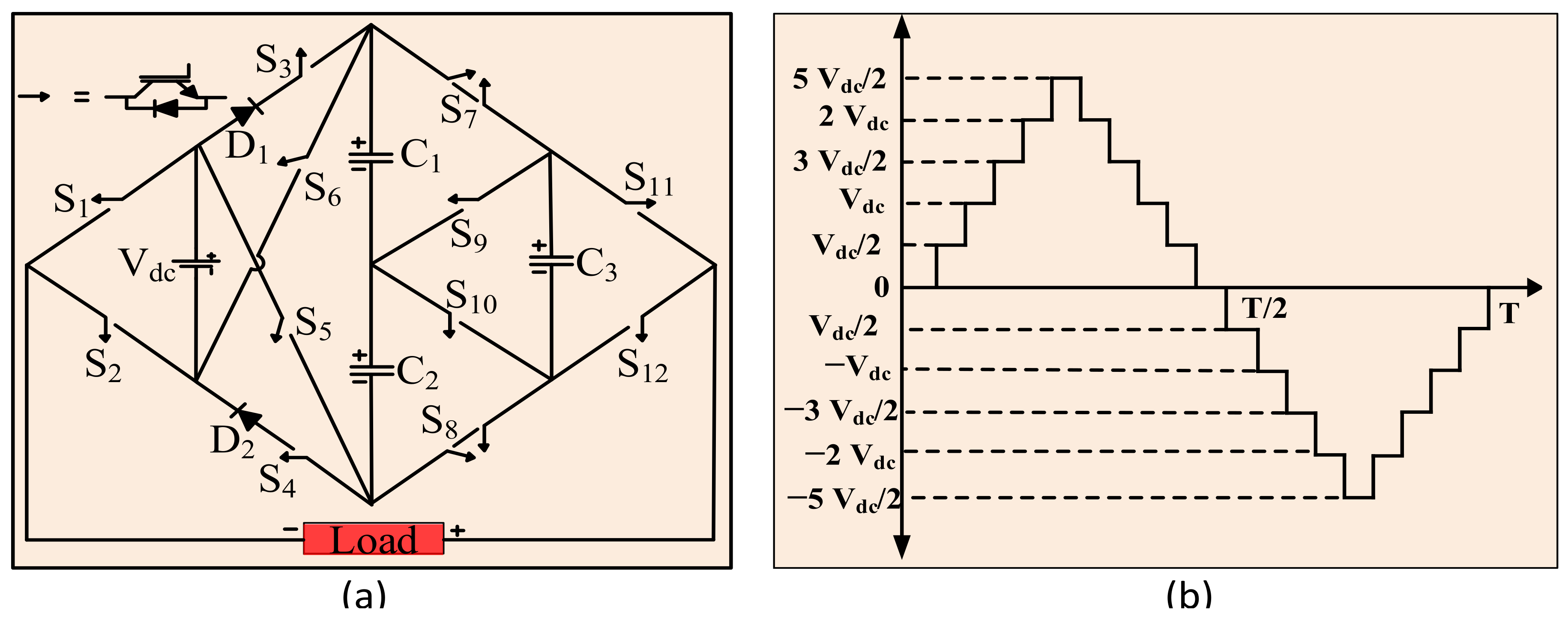
The topology and output voltage waveform for the proposed 11-level SCMLI are shown in Figure 1. An elaborate discussion on the proposed SCMLI is presented in the following subsections.
2.1. Circuit Analysis
The proposed SCMLI topology is shown in Figure 1a. It comprises 10 unidirectional switches (S1, S2, S3, S4, S5, S6, S9, S10, S11, S12), 2 bidirectional switches (S7, S8), 3 capacitors (C1, C2, C3), 2 diodes (D1, D2), and 1 DC source (Vdc). Figure 1b shows the 11-level output voltage waveform having a voltage boosting of 2.5. Here unidirectional and bidirectional are in terms of voltage. Current can flow in both directions for unidirectional switches also through reverse body diode. The capacitors are connected in the circuit in such a way that they are self-balanced and are charged to the extent that desired output voltage levels are obtained. The capacitors C1 and C2 are charged to Vdc/2, and the capacitor C3 is charged to Vdc to obtain the 11 output voltage levels as 0, ±Vdc/2, ±Vdc, ±3 Vdc/2, ±2 Vdc, and ±5 Vdc/2.
2.2. Working of the Topology for Different Voltage Levels
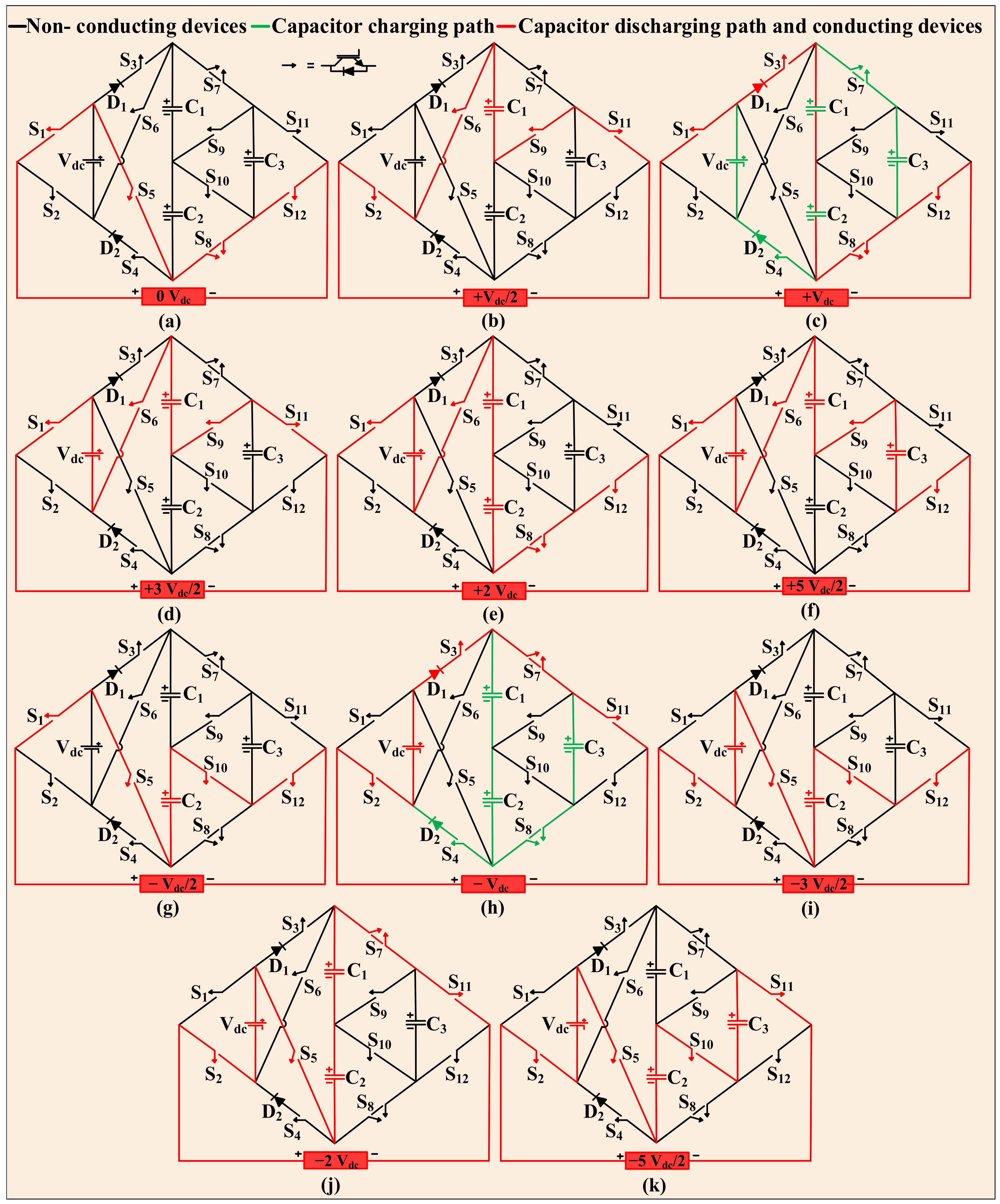
All the switching states and their respective conduction diagrams are shown in Table 1 and Figure 2, respectively. For better comprehension, the effect of different switching states has been marked. Red lines represent the conduction path, black lines represent the nonconducting path, and green lines depict the capacitor charging path. The entries “Y” and “N” indicate the on and off states of the respective switch in the table. “C”, “D”, and “NC” represent charging, discharging, and no change of the respective capacitors. The different positive output voltages can be obtained as follows:
- Zero level: Zero voltage at the load is obtained by turning the switches S1, S5, S8, and S12 on, as depicted in Figure 2a.
- 0.5 Vdc level: The required energy is supplied to the load terminals by the energy stored in C1 by turning S2, S6, S9, and S11 on, as shown in Figure 2b.
- 1 Vdc level: The energy stored in capacitors C1 and C2 is used to generate this level by turning S1, S3, S8, and S12 on. At the same time, all the capacitors are charged in this mode by turning S4 and S7 on, as shown in Figure 2c.
- 1.5 Vdc level: The required energy to generate this level at the output is obtained by the supply voltage of 1 Vdc and the energy stored in C1 by turning S1, S6, S9, and S11 on, as shown in Figure 2d.
- 2 Vdc level: The energy stored in capacitors C1 and C2 and the input supply of 1 Vdc are used to generate this level by turning S1, S6, S8, and S12 on, as shown in Figure 2e.
- 2.5 Vdc level: The energy stored in capacitors C1 and C3 and the input supply of 1 Vdc are used to generate this level by turning S1, S6, S9, and S12 on, as depicted in Figure 2f.
Likewise, in the negative half cycle, all possible levels are shown in Figure 2g–k.

Table 1.
Switching table and capacitor states for the proposed 11-level inverter.
| S1 | S2 | S3 | S4 | S5 | S6 | S7 | S8 | S9 | S10 | S11 | S12 | C1 | C2 | C3 | Output Voltage |
|---|---|---|---|---|---|---|---|---|---|---|---|---|---|---|---|
| Y | N | N | N | Y | N | N | Y | N | N | N | Y | NC | NC | NC | 0 |
| N | Y | N | N | N | Y | N | N | Y | N | Y | N | D | NC | NC | Vdc/2 |
| Y | N | Y | Y | N | N | Y | Y | N | N | N | Y | C | C | C | Vdc |
| Y | N | N | N | N | Y | N | N | Y | N | Y | N | D | NC | NC | 3 Vdc/2 |
| Y | N | N | N | N | Y | N | Y | N | N | N | Y | D | D | NC | 2 Vdc |
| Y | N | N | N | N | Y | N | N | Y | N | N | Y | D | NC | D | 5 Vdc/2 |
| Y | N | N | N | Y | N | N | Y | N | N | N | Y | NC | NC | NC | 0 |
| Y | N | N | N | Y | N | N | N | N | Y | N | Y | NC | D | NC | −Vdc/2 |
| N | Y | Y | Y | N | N | Y | Y | N | N | Y | N | C | C | C | −Vdc |
| N | Y | N | N | Y | N | N | N | N | Y | N | Y | NC | D | NC | −3 Vdc/2 |
| N | Y | N | N | Y | N | Y | N | N | N | Y | N | D | D | NC | −2 Vdc |
| N | Y | N | N | Y | N | N | N | N | Y | Y | N | NC | D | D | −5 Vdc/2 |
Y, switch on; N, switch off; C, charging; D, discharging; NC, no change.
Figure 2.
All the conduction states of the proposed topology: (a) zero output voltage; (b–f) positive half-cycle; (g–k) negative half-cycle.
Figure 2.
All the conduction states of the proposed topology: (a) zero output voltage; (b–f) positive half-cycle; (g–k) negative half-cycle.

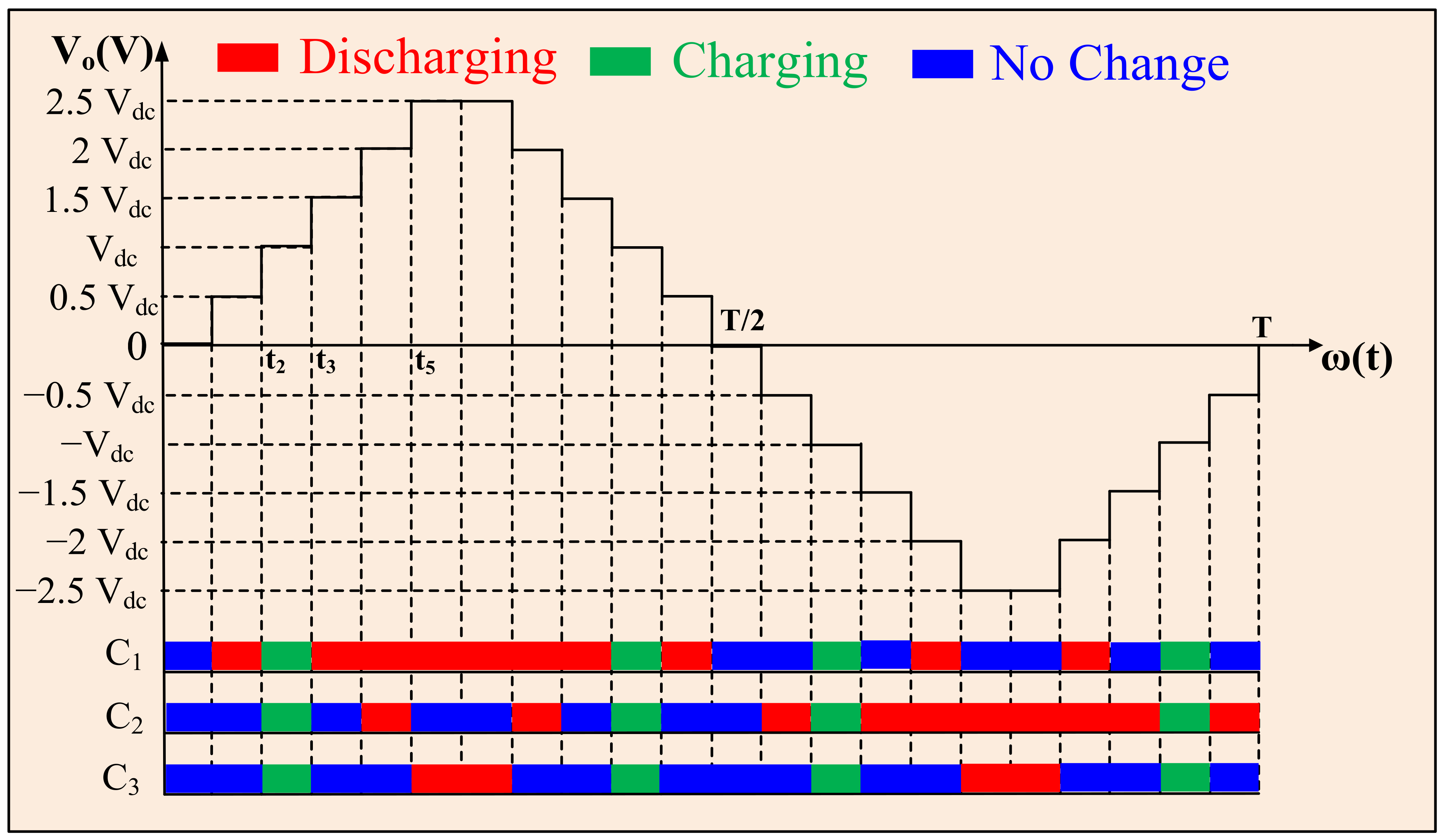
2.3. Capacitor Voltage Balance and Capacitance Calculation
All the three capacitors are self-balanced to their desired voltage levels through the parallel connection of the capacitors to the source and in series with the load at different instants. The capacitors C1, C2, and C3 are being charged during the voltage levels of +Vdc and −Vdc to 0.5 Vdc, 0.5 Vdc, and Vdc, respectively. All the charging and discharging time intervals are shown in Figure 3. Load parameters do not affect the capacitors’ charging interval as the charging circuit of the topology has only diodes, switches, and capacitors [20]. Hence, the charging and discharging intervals for the capacitors are equal in a cycle. Therefore, the self-voltage balance of all the capacitors is maintained irrespective of the loading condition. The largest discharging period (LDP), nominal frequency, least voltage ripple, and maximum fundamental load current are used to calculate the optimum value of the capacitors. Using LDP for capacitor C1, which is the same as that of capacitor C2, i.e., [t3, T/2 − t3], the maximum discharging amount during this time interval is expressed in (1).
where f is the output voltage frequency and iL is the load current.
The largest discharging period for C3 is [t5, T/2 − t5]. Hence, the maximum discharging amount during this interval can be expressed as
From Equations (1) and (2), the values of C1, C2, and C3 can be calculated as
Thus, by taking maximum allowable ripple voltage (∆Vc) equal to 10% of the corresponding capacitor voltage, the solution of Equations (3) and (4) give the optimum value of all the capacitors.
2.4. Power Loss Analysis
Three types of losses are considered for the proposed SCMLI topology, including charging or ripple loss, conduction loss, and switching loss occurring in the system.
2.4.1. Ripple or Charging Loss (PR)
The ripple or charging loss is the loss associated with the charging of the capacitor. The magnitude of the charging current flowing through the capacitor during this period depends upon the voltage difference between the present value of the capacitor voltage and the desired value of the capacitor voltage. The ripple loss of the capacitors during a fundamental cycle can be expressed as
where n is the number of capacitors present in the circuit, f is the fundamental frequency, and is the capacitor voltage ripple of the nth capacitor. can also be obtained from the following equation:
where duration [0, t] is the largest discharging period and iC is the capacitor charging current.
2.4.2. Ohmic Loss (PO)
The ohmic loss is caused due to the internal resistances of the devices entering the conduction path. PO for different levels can be calculated by the equivalent circuit diagram for that level. Thus, the total ohmic loss of the topology can be obtained by considering all the voltage levels. Ohmic loss can be expressed as
where is the load current; is the on-state switch resistance; is the diode resistance; is the internal resistance of the capacitor; and n, m, and p are the numbers of switches, diodes, and capacitors present in the conduction path of the corresponding level.
2.4.3. Switching Loss (PS)
Switching losses occur during the switching activity of the switches. Assuming the switch voltage and current to be linear at the time of switching, the switching power loss during the turn-on process can be expressed as
Loss of power during switching off process can be expressed as
where I is the current flowing through the switch during the turn-on time, is the current flowing through the switch during the turn-off time, ‘f’ is the switching frequency, and is the withstanding voltage of the switch. Total switching loss of the topology can be calculated by multiplying the number of the on () switching states and number of the off switching states () in one complete cycle with (8) and (9), resulting in (10):
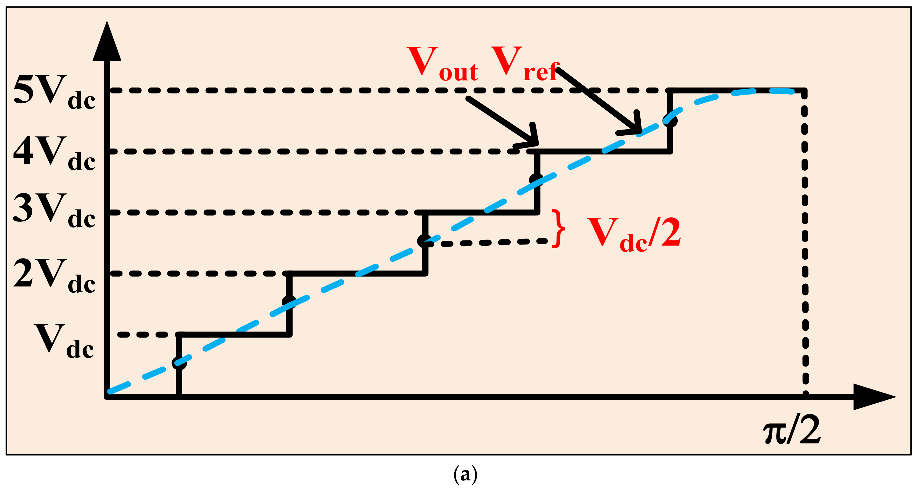
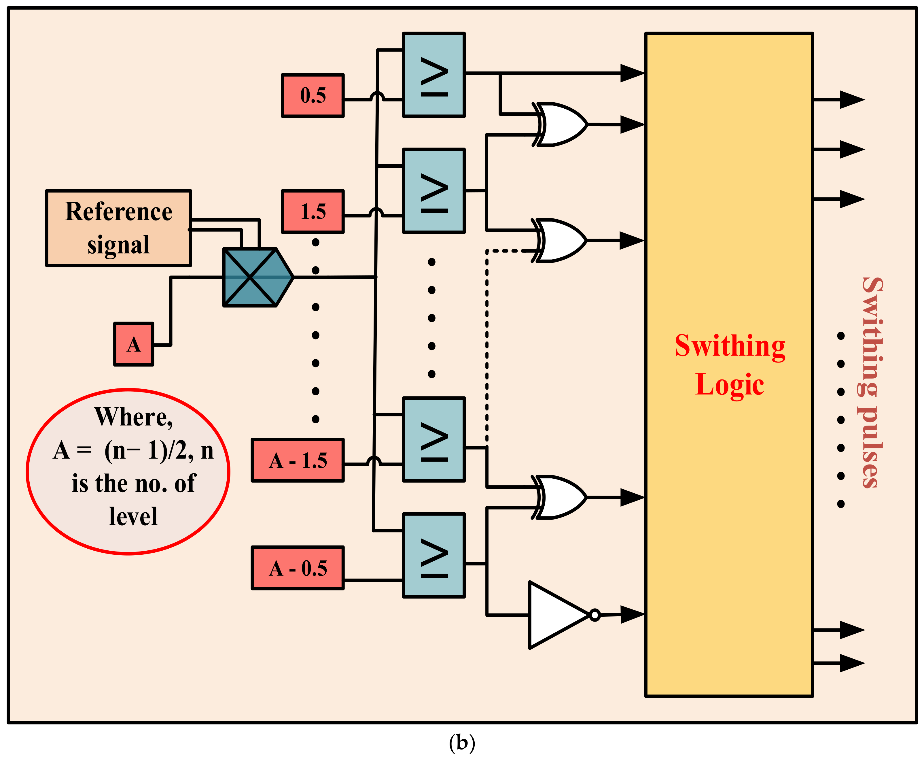
2.5. Nearest Level Control (NLC)
Numerous modulation schemes have been tested and used for multilevel inverters. The nearest level control is a low-switching-frequency PWM technique for which the complexity in implementation is lesser for a higher number of levels [21]. NLC is used here for the proposed topology to control the switches so that the desired output waveform is obtained. In NLC, the reference sinusoidal waveform is compared with the desired output waveform to obtain a sampled waveform. The waveform generated is then rounded off to the nearest level and compared according to the switching logic given in Table 1 to produce switching signals for the corresponding IGBTs. The working principle of the NLC is shown in Figure 4a,b. The symbol “A” in the figure corresponds to 5 for this 11-level topology. The amplitude of the reference signal (sine wave) is also 5, and its frequency is taken to be 50 Hz.
3. Comparative Analysis
Comparison of the proposed 11-level inverter with recently published 11-level topologies was carried out in order to show its advantages over these topologies. The detailed comparison is shown in Table 2 on the basis of the number of switches (Nsw), number of diodes (Nd), number of DC sources (Ndc), number of capacitors (Nc), the voltage gain of the converter, TSVpu, and efficiency (η). Total standing voltage (TSV) is the sum of all the maximum voltage stresses across all the switches. It is the deciding factor for the voltage rating of the switches to be used in the topology. TSVpu is the ratio of TSV to the peak value of AC output voltage. The proposed topology and the one presented in [16] have the minimum TSVpu. The proposed topology needs 14 IGBTs, but as it has two bidirectional switches and six unidirectional switches, the number of drivers required is reduced to nine. Among single DC source topologies, that presented in [16] has fewer switches than the proposed one, but it uses five capacitors as compared to three in the proposed topology. Further, it has no voltage-boosting ability. Only the proposed topology has the boosting feature with a gain of 2.5. Topologies presented in [18,21] use three DC sources, while the topology presented in [22] uses two DC sources. In terms of efficiency, the proposed topology stands better than these topologies except that of [16]. The efficiency of the proposed topology is quite high at 96.75%.
4. Results and Discussion
In this section, simulation results and hardware results of the proposed 11-level inverter topology are presented for different loading conditions.
4.1. Simulation Results
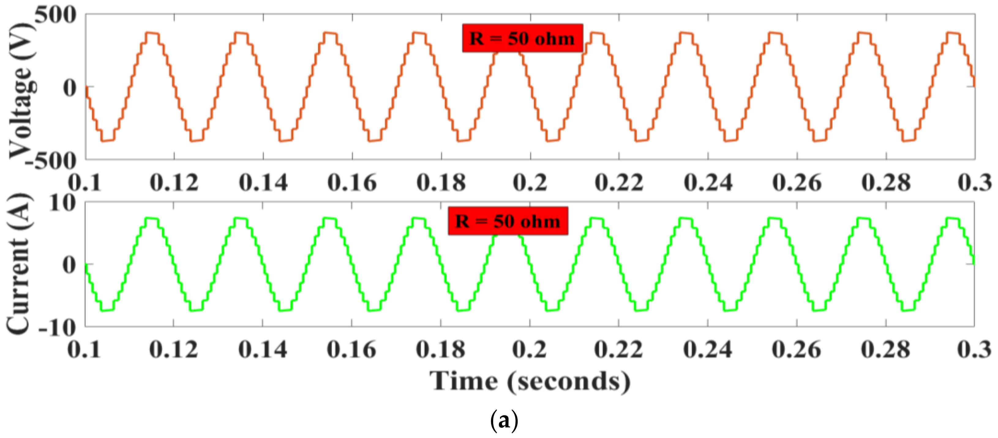
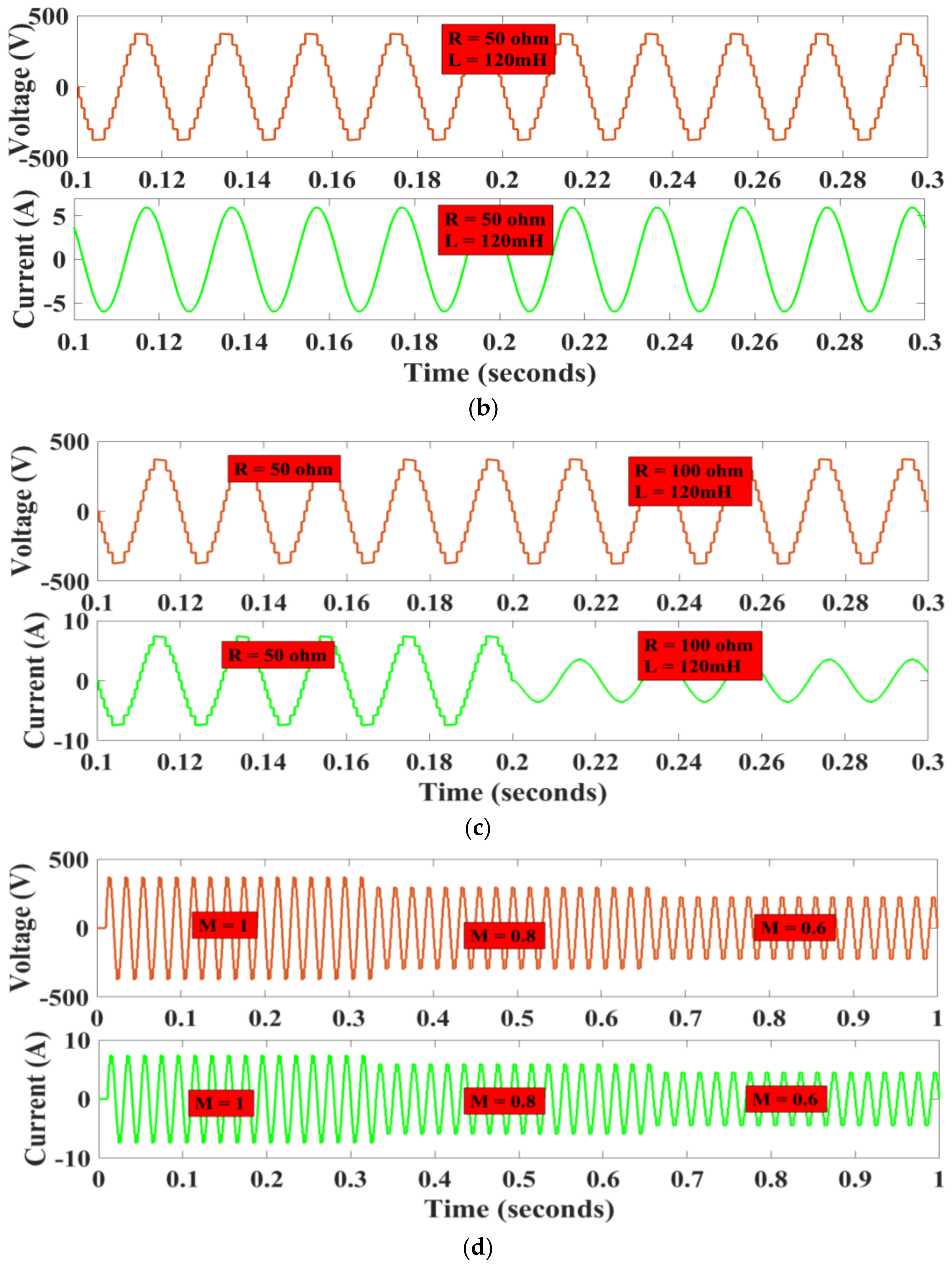
The proposed topology was simulated using MATLAB/Simulink. Figure 5 shows various simulation results obtained for the topology. Output voltage and current waveforms of the proposed 11-level inverter for the purely resistive load (R = 50 Ω) are shown in Figure 5a. Figure 5b shows the voltage and current waveform for RL load (R = 50 Ω, L = 120 mH). The voltage and current plot for dynamic load change from R = 50 Ω to R = 100 Ω and L = 120 mH is shown in Figure 5c. Figure 5d shows the effect of change in modulation values (M = 1.0, 0.8, 0.6). The smooth results showing a sudden change in load and modulation index verify the performance of the proposed inverter. Different parameters taken for the simulation are shown in Table 3.
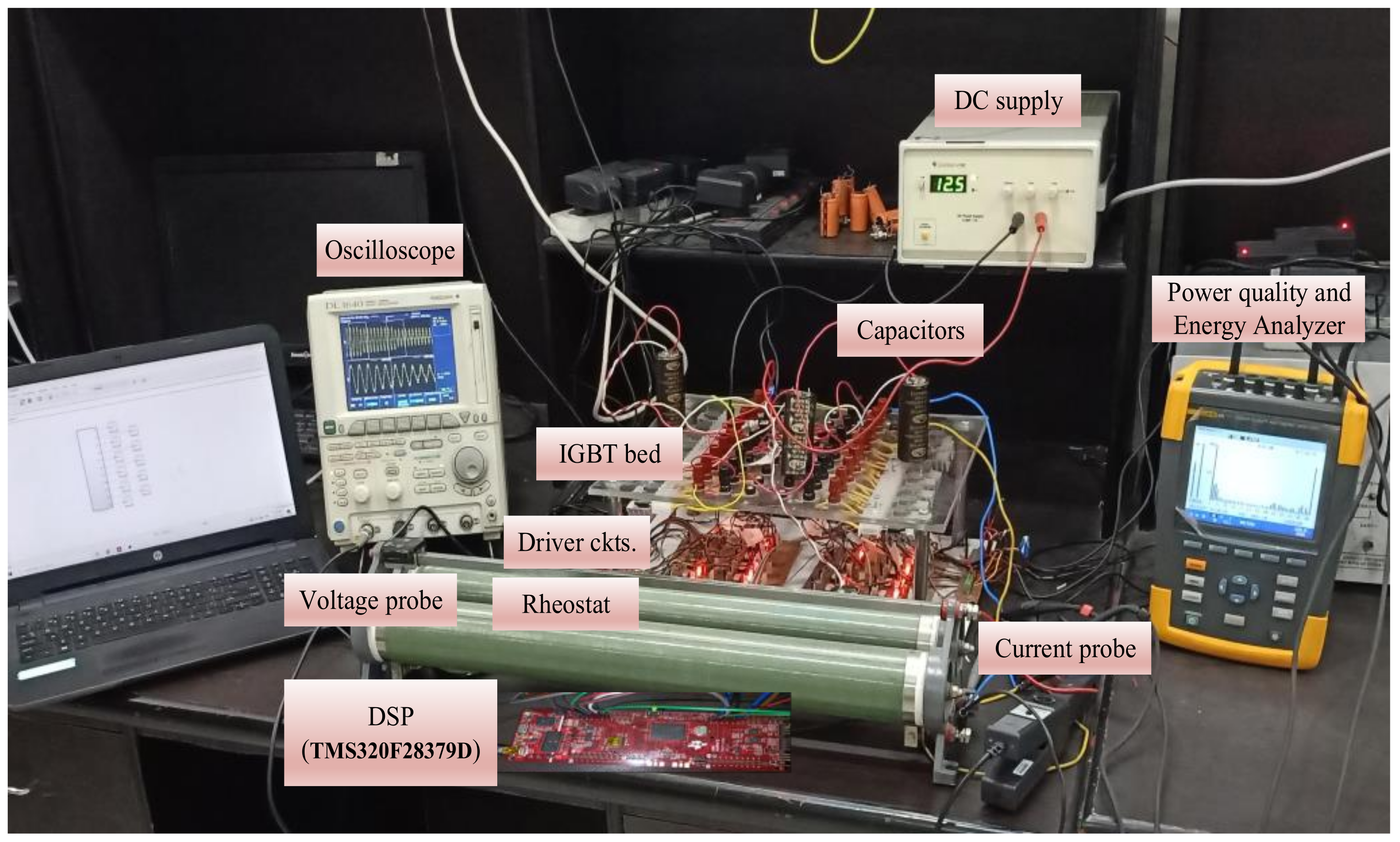
4.2. Hardware Results
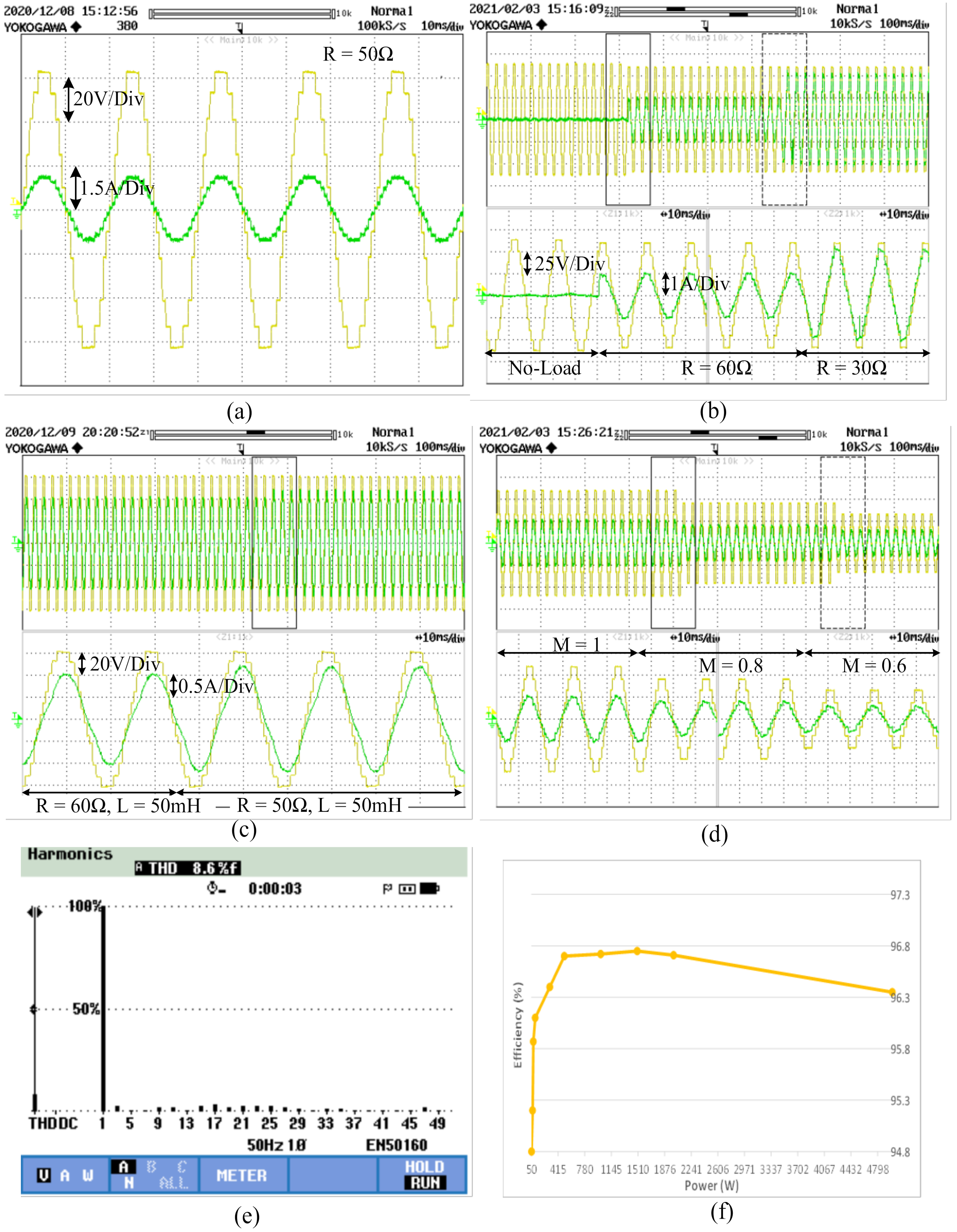
A hardware prototype, shown in Figure 6, was developed to test the viability of the proposed 11-level inverter. An insulated-gate bipolar transistor (IGBT) (FGA25N120) was used to build the circuit. TLP-250H-based gate driver circuit was used for generating gate signals to individual IGBTs. Fundamental switching nearest level control (NLC) scheme was used to produce gate signals. The NLC scheme was implemented with the help of a digital signal processor (TMS320F28379D) for the proposed inverter. A FLUKE 435 series II power quality and energy analyzer was used for measuring experimental THD and efficiency percentages of the proposed MLI. Experimental parameters are shown in Table 4. Figure 7a shows the 11-level output voltage with a peak voltage of around 62 volts and a current peak of 1.2 A for a resistive load of 50 Ω, which validates the voltage gain of 2.5 for an input voltage of 25 V. As the load is suddenly changed from no load to 60 Ω to 30 Ω, the magnitude of load current changes from 0 A to 1 A to 2 A as shown in Figure 7b. Figure 7c represents a dynamic change in the power factor. The load current is steady even after this sudden load change, and the output voltage is also unaffected. The proposed inverter was also tested for different modulation indices that are shown in Figure 7d. It is seen that as the modulation index is changed from 1 to 0.8 to 0.6, the number of output levels is accordingly reduced from 11 to 9 to 7. The output voltage THD is shown in Figure 7e. Output voltage THD was found to be 8.6% when a load of 50 Ω and 100 mH was taken. The efficiency curve of the proposed circuit was obtained by plotting the efficiency at different loads versus the output power using the power quality and energy analyzer, as represented in Figure 7f. The maximum efficiency achieved is 96.75% at an output power of 1500 watts, which decreases as the output power is increased [24,25]. Figure 8 shows the effect of modulation change on the THD of the proposed inverter. Simulation of the inverter was completed at different modulation indices and the THD was obtained. As the modulation index is decreased, THD increases and the number of levels is also affected. Eleven levels are obtained at the output for modulation index of 0.92–1, which decreases to nine for modulation index of 0.72–9 and then to seven for modulation index of 0.6–0.7.
5. Conclusions
A switched-capacitor MLI topology with the detailed operating principle and circuit analysis is proposed. It has 2.5 times voltage boosting, and the maximum voltage stress across the switches is restricted to twice the input voltage, which results in reduced TSV of the proposed inverter. All the capacitors are self-balanced, which simplifies the control complexity. A simple fundamental modulation technique, i.e., NLC, is implemented to generate the gating pulses for IGBTs. Hardware results validate the performance of the proposed topology under different dynamic loading conditions. A thorough comparison reflects the efficacy of the proposed topology over the recently published 11-level topologies. The output voltage THD of the proposed inverter is 8.6%. The maximum efficiency achieved for the converter is 96.75%.
Author Contributions
Conceptualization, M.R.H., A.S., M.T. (Mohd Tariq), and M.T. (Mohammad Tayyab); formal analysis, M.R.H., A.S., I.K., M.T. (Mohd Tariq), and M.T. (Mohammad Tayyab); funding acquisition, M.T. (Mohd Tariq) and W.A.; investigation, M.R.H., A.S., I.K., M.T. (Mohd Tariq), M.T. (Mohammad Tayyab), and W.A.; methodology, M.R.H., A.S., I.K., M.T. (Mohd Tariq), M.T. (Mohammad Tayyab) and W.A.; project administration, M.T. (Mohd Tariq) and W.A.; supervision: A.S. and M.T. (Mohd Tariq); writing—original draft, M.R.H. and A.S.; writing—review and editing, I.K., M.T. (Mohd Tariq), M.T. (Mohammad Tayyab), and W.A. All authors have read and agreed to the published version of the manuscript.
Funding
The authors extend their appreciation to the Deputyship for Research Innovation, Ministry of Education in Saudi Arabia, for funding this work through the project number “375213500”. The authors acknowledge the financial support provided from the Collaborative Research Grant Scheme (CRGS) Project CRGS/MOHD TARIQ/01 and CRGS/MOHD TARIQ/02 sponsored by the Capability Systems Centre, UNSW, Canberra, to the Hardware-In-the-Loop (HIL) Lab, Department of Electrical Engineering, Aligarh Muslim University, India, and the technical support provided by the Non-Conventional Energy (NCE) Lab, Department of Electrical Engineering, Aligarh Muslim University, India.
Data Availability Statement
Not applicable.
Conflicts of Interest
The authors declare no conflict of interest.
References
- Sandeep, N.; Yaragatti, U.R. Design and implementation of a sensorless multilevel inverter with reduced part count. IEEE Trans. Power Electron. 2017, 32, 6677–6683. [Google Scholar] [CrossRef]
- Tayyab, M.; Sarwar, A.; Tariq, M.; Chakraborty, R.K.; Ryan, M.J. Hardware-in-the-loop implementation of projectile target search algorithm for selective harmonic elimination in a 3-phase multilevel converter. IEEE Access 2020, 9, 30626–30635. [Google Scholar] [CrossRef]
- Sathik, M.J.; Vijayakumar, K.; Member, S. Compact Switched Capacitor Multilevel Inverter (CSCMLI) with self voltage balancing and boosting ability. IEEE Trans. Power Electron. 2018, 34, 4009–4013. [Google Scholar] [CrossRef]
- Naik, B.S.; Suresh, Y.; Venkataramanaiah, J.; Panda, A.K. A hybrid nine-level inverter topology with boosting capability and reduced component count. IEEE Trans. Circuits Syst. II Express Briefs 2021, 68, 316–320. [Google Scholar] [CrossRef]
- Hussan, M.R.; Ansari, M.K.; Lodi, K.A.; Sarwar, A.; Tariq, M.; Husain, H. Genetic algorithm based optimal operation of a modified H-bridge single phase multilevel inverter. In Proceedings of the 2019 International Conference on Power Electronics, Control and Automation (ICPECA 2019), New Delhi, India, 16–17 November 2019. [Google Scholar] [CrossRef]
- Prabaharan, N.; Palanisamy, K. A comprehensive review on reduced switch multilevel inverter topologies, modulation techniques and applications. Renew. Sustain. Energy Rev. 2017, 76, 1248–1282. [Google Scholar] [CrossRef]
- Shiva Naik, B.; Suresh, Y.; Venkataramanaiah, J. Experimental verification of a hybrid multilevel inverter with voltage-boosting ability. Int. J. Circuit Theory Appl. 2020, 48, 420–434. [Google Scholar] [CrossRef]
- Kim, K.M.; Han, J.K.; Moon, G.W. A High step-up switched-capacitor 13-level inverter with reduced number of switches. IEEE Trans. Power Electron. 2021, 36, 2505–2509. [Google Scholar] [CrossRef]
- Sandeep, N. A 13-level switched-capacitor-based boosting inverter. IEEE Trans. Circuits Syst. II Express Briefs 2021, 68, 998–1002. [Google Scholar] [CrossRef]
- Sedaghati, F.; Majareh, S.H.L. A multilevel inverter based on cascade connection of submultilevel units with reduced switch count. Int. J. Circuit Theory Appl. 2019, 47, 1152–1172. [Google Scholar] [CrossRef]
- Rana, R.A.; Patel, S.A.; Muthusamy, A.; Lee, C.W.; Kim, H.J. Review of multilevel voltage source inverter topologies and analysis of harmonics distortions in FC-MLI. Electronics 2019, 8, 1329. [Google Scholar] [CrossRef] [Green Version]
- Hussan, M.R.; Sarwar, A.; Siddique, M.D.; Mekhilef, S.; Ahmad, S.; Sharaf, M.; Zaindin, M.; Firdausi, M. A novel switched-capacitor multilevel inverter topology for energy storage and smart grid applications. Electronics 2020, 9, 1703. [Google Scholar] [CrossRef]
- Xun, Z.; Ding, H.; He, Z. A novel switched-capacitor inverter with reduced capacitance and balanced neutral-point voltage. Electronics 2021, 10, 947. [Google Scholar] [CrossRef]
- Hussan, M.R.; Sarwar, A.; Siddique, M.D.; Iqbal, A.; Alamri, B. A cross connected asymmetrical switched-capacitor multilevel inverter. IEEE Access 2021, 9, 96416–96429. [Google Scholar] [CrossRef]
- Lin, W.; Zeng, J.; Hu, J.; Junfeng, L. Hybrid nine-level boost inverter with simplified control and reduced active devices. IEEE J. Emerg. Sel. Top. Power Electron. 2021, 9, 2038–2050. [Google Scholar] [CrossRef]
- Panda, N.; Das, B.; Chakrabarti, A.; Kasari, P.R.; Bhattacharaya, A.; Chatterjee, D. A new grid interactive eleven-level hybrid inverter topology for medium-voltage application. IEEE Trans. Ind. Appl. 2020, 57, 869–881. [Google Scholar] [CrossRef]
- Priyadarshi, A.; Kar, P.K.; Karanki, S.B. A single source transformer-less boost multilevel inverter topology with self-voltage balancing. IEEE Trans. Ind. Appl. 2020, 56, 3954–3965. [Google Scholar] [CrossRef]
- Siddique, M.D.; Mekilef, S.; Shah, N.M.; Memon, M.A. Optimal design of a new cascaded multilevel inverter topology with reduced switch count. IEEE Access 2019, 7, 24498–24510. [Google Scholar] [CrossRef]
- Hosseinzadeh, M.A.; Sarebanzadeh, M.; Rivera, M.; Babaei, E.; Wheeler, P. A reduced single-phase switched-diode cascaded multilevel inverter. IEEE J. Emerg. Sel. Top. Power Electron. 2021, 9, 3556–3569. [Google Scholar] [CrossRef]
- Sun, X.; Wang, B.; Zhou, Y.; Wang, W.; Du, H.; Lu, Z. A single DC source cascaded seven-level inverter integrating switched-capacitor techniques. IEEE Trans. Ind. Electron. 2016, 63, 7184–7194. [Google Scholar] [CrossRef]
- Bana, P.R.; Panda, K.P.; Panda, G. Power quality performance evaluation of multilevel inverter with reduced switching devices and minimum standing voltage. IEEE Trans. Ind. Inform. 2020, 16, 5009–5022. [Google Scholar] [CrossRef]
- Alishah, R.S.; Hosseini, S.H.; Babaei, E.; Sabahi, M. A new general multilevel converter topology based on cascaded connection of submultilevel units with reduced switching components, DC sources, and blocked voltage by switches. IEEE Trans. Ind. Electron. 2016, 63, 7157–7164. [Google Scholar] [CrossRef]
- Khan, M.N.H.; Forouzesh, M.; Siwakoti, Y.P.; Li, L.; Blaabjerg, F. Switched capacitor integrated (2n + 1)-level step-up single-phase inverter. IEEE Trans. Power Electron. 2020, 35, 8248–8260. [Google Scholar] [CrossRef]
- Siddique, M.D.; Reddy, B.P.; Iqbal, A.; Mekhilef, S. Reduced switch count-based N-level boost inverter topology for higher voltage gain. IET Power Electron. 2020, 13, 3505–3509. [Google Scholar] [CrossRef]
- Reddy, B.P.; Siddique, M.D.; Iqbal, A.; Mekhilef, S.; Rahman, S.; Maroti, P.K. 7L-SCBI topology with minimal semiconductor device count. IET Power Electron. 2020, 13, 3199–3203. [Google Scholar] [CrossRef]
Figure 1.
Proposed topology: (a) circuit diagram; (b) 11-level output voltage.

Figure 3.
Staircase output with capacitor voltage pattern.

Figure 4.
Nearest level control: (a) level generation method; (b) working of NLC.


Figure 5.
Output voltage and current waveforms of the proposed 11-level inverter for (a) resistive load of 50 Ω, (b) RL load (R = 50 Ω, L = 120 mH), (c) dynamic load change from R = 50 Ω to R = 100 Ω and L = 120 mH, and (d) change in modulation from M = 1.0 to M = 0.8 to M = 0.6.
Figure 5.
Output voltage and current waveforms of the proposed 11-level inverter for (a) resistive load of 50 Ω, (b) RL load (R = 50 Ω, L = 120 mH), (c) dynamic load change from R = 50 Ω to R = 100 Ω and L = 120 mH, and (d) change in modulation from M = 1.0 to M = 0.8 to M = 0.6.


Figure 6.
Experimental Setup.

Figure 7.
Output voltage and current waveform of the proposed 11-level inverter for (a) resistive load of 50 Ω, (b) dynamic load change from no load to 60 Ω to 30 Ω, (c) dynamic load change from 60 Ω–50 mH to 50 Ω–50 mH, (d) change in modulation from M = 1.0 to M = 0.8 to M = 0.6, (e) THD of the output voltage, and (f) efficiency in different loading conditions.

Figure 8.
Effect of modulation change on THD of the inverter.

Table 2.
Comparison of the proposed MLI with recent 11-level topologies.
| 11-Level MLI | Nsw | Ndr | Nd | Ndc | Nc | Gain | TSVp.u | Efficiency (%) |
|---|---|---|---|---|---|---|---|---|
| [16] | 12 | 6 | 0 | 1 | 5 | 1 | 3.0 | 97.32 |
| [18] | 8 | 7 | 0 | 3 | 1 | 1 | 4.4 | - |
| [21] | 9 | 9 | 1 | 3 | 1 | 1 | 4.2 | 96 |
| [22] | 10 | 10 | 4 | 2 | 2 | 1 | 5.2 | 93.85 |
| [23] | 17 | 17 | 1 | 1 | 5 | 1 | 3.33 | 96.5 |
| Proposed | 14 | 9 | 2 | 1 | 3 | 2.5 | 3.0 | 96.75 |
Table 3.
Simulation parameters.
| DC voltage sources | 150 V |
| Capacitors | 4700 μF, 200 V, 2200 μF, 200 V |
| Load resistance | 50 Ω, 100 Ω |
| Load inductance | 120 mH |
| Output frequency | 50 Hz |
| Switching frequency | 50 Hz |
Table 4.
Parameters for experimental validation.
| DC Voltage Sources | 25 V (Vdc) |
| Capacitors | 4700 μF, 100 V, 2200 μF, 100 V |
| Load Resistance | 30 Ω, 50 Ω, 60 Ω |
| Load Inductance | 50 mH |
| Output frequency | 50 Hz |
| Switching frequency | 50 Hz |
Publisher’s Note: MDPI stays neutral with regard to jurisdictional claims in published maps and institutional affiliations. |
© 2021 by the authors. Licensee MDPI, Basel, Switzerland. This article is an open access article distributed under the terms and conditions of the Creative Commons Attribution (CC BY) license (https://creativecommons.org/licenses/by/4.0/).
Share and Cite
MDPI and ACS Style
Hussan, M.R.; Sarwar, A.; Khan, I.; Tariq, M.; Tayyab, M.; Alhosaini, W. An Eleven-Level Switched-Capacitor Inverter with Boosting Capability. Electronics 2021, 10, 2262. https://doi.org/10.3390/electronics10182262
AMA Style
Hussan MR, Sarwar A, Khan I, Tariq M, Tayyab M, Alhosaini W. An Eleven-Level Switched-Capacitor Inverter with Boosting Capability. Electronics. 2021; 10(18):2262. https://doi.org/10.3390/electronics10182262
Chicago/Turabian StyleHussan, Md Reyaz, Adil Sarwar, Irfan Khan, Mohd Tariq, Mohammad Tayyab, and Waleed Alhosaini. 2021. "An Eleven-Level Switched-Capacitor Inverter with Boosting Capability" Electronics 10, no. 18: 2262. https://doi.org/10.3390/electronics10182262
Note that from the first issue of 2016, this journal uses article numbers instead of page numbers. See further details here.