
Electric and Magnetic Design of a Deployable WPT System for Industrial and Defense UAV Applications

Laboratory of Systems with Innovative Antennas, University Politehnica of Bucharest, 061071 Bucharest, Romania
*
Author to whom correspondence should be addressed.
Electronics 2021, 10(18), 2252; https://doi.org/10.3390/electronics10182252
Submission received: 27 July 2021
/
Revised: 3 September 2021
/
Accepted: 6 September 2021
/
Published: 13 September 2021
(This article belongs to the Special Issue Advanced Design of RF/Microwave Circuit)
Abstract
:The following paper presents a highly efficient wireless power transfer (WPT) system for unmanned aerial vehicle (UAV) applications. The proposed system is designed as a deployable landing pad, where UAVs can be efficiently charged at distances up to 20 cm, while the UAV is landing. The operation frequency is 50 kHz. The current work presents two major contributions that help improve this aspect: a novel RX charging pad geometry and an unconventional design of a low-voltage, high-power DC–AC inverter using discrete MOSFET transistors. Both the pad’s geometry and the inverter are designed specifically for UAV applications. The input DC to output AC system efficiency peaks at approximately 95%. The peak efficiency is obtained at power transfers of 625 W. A major difference between the present design and traditionally used state-of-the-art systems is the low DC supply voltage requirement of just 24 V, compared with typical values that range from 50 up to 300 V at similar output power.
1. Introduction
During recent years, the importance of UAV systems has grown exponentially, both in civil and defense applications. The development and evolution of UAV systems is summarized in [1]. Their popularity is due to the fact that they represent an exceptional candidate for a vast number of applications, such as: video surveillance [2,3], defense [4], geological observations [5], SAR (synthetic aperture radar) [6], etc. In applications in which UAVs are required to function continuously, such as the latest trend of pollination drones, the autonomy of the system becomes crucial [7]. Such systems would greatly benefit from an accessible and remote charging station that can be easily transported and deployed. WPT systems offer several advantages over electrically connected contact-based charging systems [8], among which is a safe operation mode even in wet or dirty environments [9,10] that may be remotely accessed in warzones or hazardous environments or in large areas which are not easily accessible by land vehicles (e.g., forests, mountains, canyons, etc.). The solution proposed in this paper addresses an efficient power transfer in the 200 W–1 kW range [11], at charging distances between 10 and 20 cm. The peak system efficiency of 95% is obtained at 10 cm with an output power of 625 W. In prior work, an electric vehicle (EV) charging system is presented [12], with similar efficiencies, and power transfers of over 3.3 kW—when operating at the same height of 10 cm. However, the authors use ferrite bars for both transmitter (Tx) and receiver (Rx) charging pads to increase coupling. This is not a practical solution for UAVs that have weight limitations (on the Rx side). The Rx pad proposed in this paper weights less than 300 g, compared to the 15 kg Tx pad. It is obvious that for the UAV applications, the solution using ferrites for Rx must be discarded. Eliminating the ferrite bars on the Rx side will result in field leakage throughout the UAV and should be taken into consideration when designing the chassis.
The rest of the paper is organized as follows: Section 2 of this paper consists of a brief introduction to WPT basics, where the main concepts and notations used throughout the article are explained and defined. Section 3 presents the magnetic design of the Tx and Rx pads of the prototype, taking into account the optimal trade-off between weight, cost, power transfer, charging area, and efficiency. Further, in Section 4, a VLF (very low frequency) driving system based on Class-E RF power amplifiers (PA) is described. Section 5 provides results obtained from a wide set of experiments. Finally, Section 6 summarizes the paper.
2. The WPT System
2.1. Non-Resonant WPT Systems
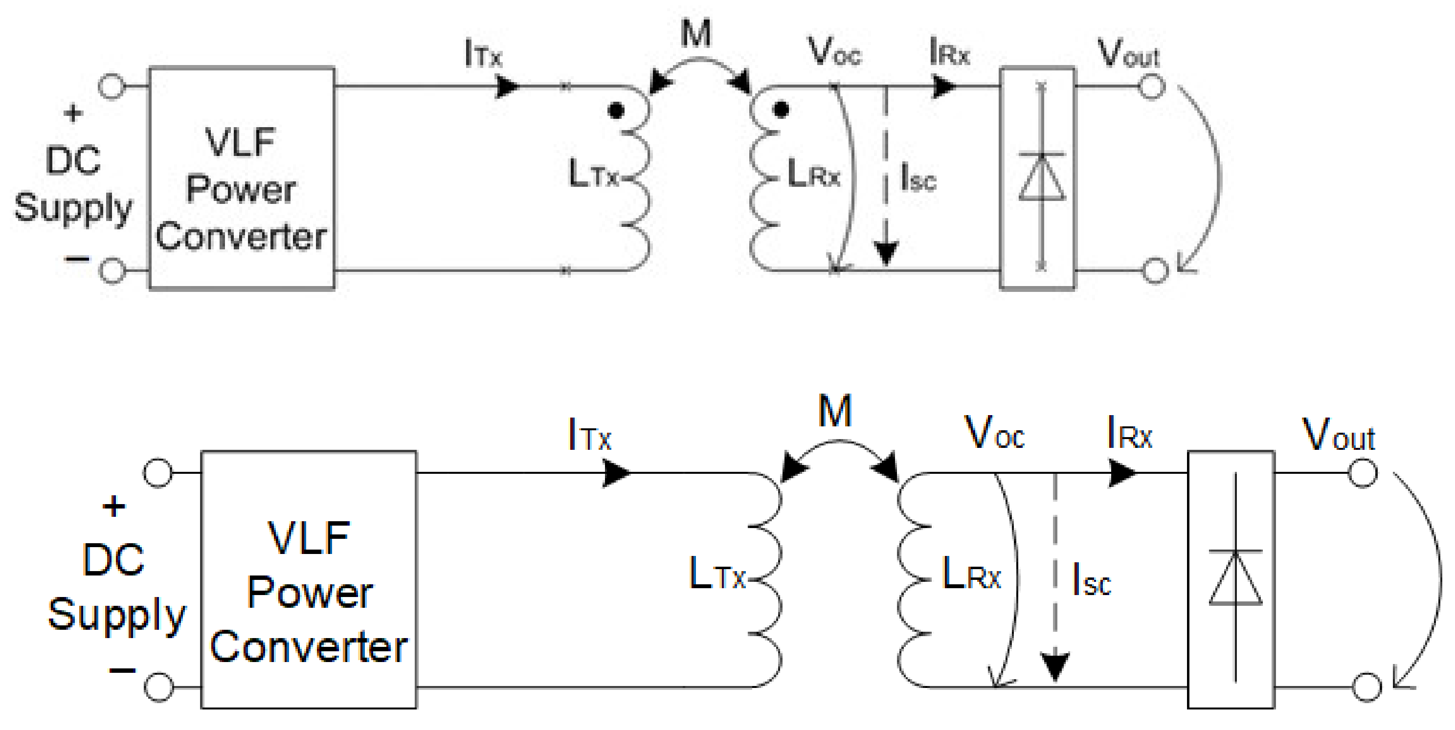
A typical system design of a WPT system is shown in Figure 1. The VLF block converts DC power to a VLF signal, with typical frequencies of tens of kHz. and are the Tx and Rx coils’ inductance, respectively. M is the mutual inductance between and , is current through when the terminals are shorted, and is the voltage when the coils’ terminals are left open. is a DC voltage proportional to the received power and load impedance.
2.2. Resonant WPT Systems
By using resonant techniques, the output power of a WPT system can be expressed as the product between and a factor, Q, that depends on the loaded quality factor [14] of the receiver and the compensation topology (which can be series, parallel, or complex). Therefore, when using a resonant LC compensation network, the maximum transferred power is increased by a factor of 2Q [15]:
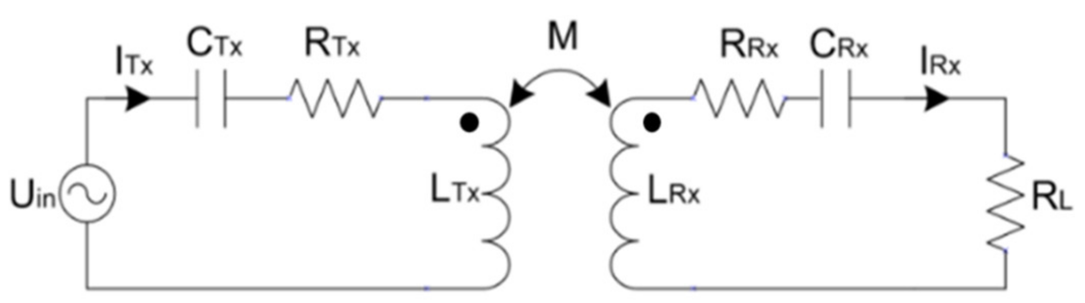
where is the coupling factor, and is the output voltage of the Tx. Equation (2) shows that the output power can be increased if either the coupling factor or the loaded quality factor increases, for a given input power. If the frequency is increased, a higher can be obtained [16]; however, copper and switching losses also increase. The configuration is presented in Figure 2, where and represent the resistive losses of the Tx and Rx coils respectively, and and represent the Tx and Rx capacitors, respectively. A drawback of the series–series configuration is that maximum power transfers can only be obtained at off-resonant frequencies, thus there will always be a trade-off between maximum power output and efficiency.
It was considered that for the application addressed in this work, the most suited configuration of the two Tx and Rx LC resonators is series–series. The main reason is that Li-ion batteries have multiple charging stages that require either a constant voltage or a constant current, resulting in a variable load impedance. This makes the series–series configuration a superior choice, because the primary capacitance,, is independent of mutual coupling or load impedance, unlike the series–parallel configuration. A more detailed analysis on this topic can be found in [17,18]. An important issue is that for a weak coupling between Rx and Tx, large currents are generated at resonance which may permanently damage the transmission system.
Considering that the network is supplied with a harmonic voltage at a frequency equal to the resonant frequency of the two LC series networks, the imaginary component of the impedance vanishes. The solution for the primary and secondary currents, and respectively, becomes:
Due to the “” factor, the waveform at the Rx is 90 degrees offset from the Tx waveform, and this will be noticed later on in both the Spice simulations and experimental results. Another important observation is that if the system is weakly coupled, so that M becomes close to 0, the primary current will become extremely large and can potentially damage the system. This paramount observation will be emphasized in the experimental results section. Alongside power transfer, another important parameter in WPT systems is the transfer efficiency, defined as:
Therefore, the transfer efficiency can be re-written as:
Figure 3 shows the simulated efficiency as a function of the load resistance. For illustrative purposes, the other parameters were set to: , , and .
By solving the null derivative equation and imposing a negative second-order derivative the maximum efficiency requires that:
where represents the product between the transmitter and receiver quality factors, and , respectively. By introducing the notation , the maximum obtainable power transfer efficiency becomes:
Equation (8) proves that by using resonant techniques, the efficiency can be greatly boosted, even when weakly coupled. However, by analyzing Equation (8), one would be inclined to increase the operating frequency of the system to further increase the quality factor, and hence the efficiency. In practice, by increasing the operating frequency, the system losses (i.e., hysteresis losses in the ferrite bars, skin effect losses, switching losses, etc.) also increase. The operating frequency was chosen to be 50 kHz based on the materials and components used.
3. Charging Pads
3.1. Tx Charging Pad Analysis
In this section, we present a short analysis of both the electrical and magnetic design of the TX pad. The type of LC topology used is series–series. For such a topology, high coupling may cause a double resonance around the initial resonant frequency. This is similar to the effect found in capacitive coupled band-pass filters, which when highly coupled begin to have a double resonance. However, if the resonant peaks are not sharp, this translates into a single larger bandwidth allowing a lower tolerance of the series capacitor value.
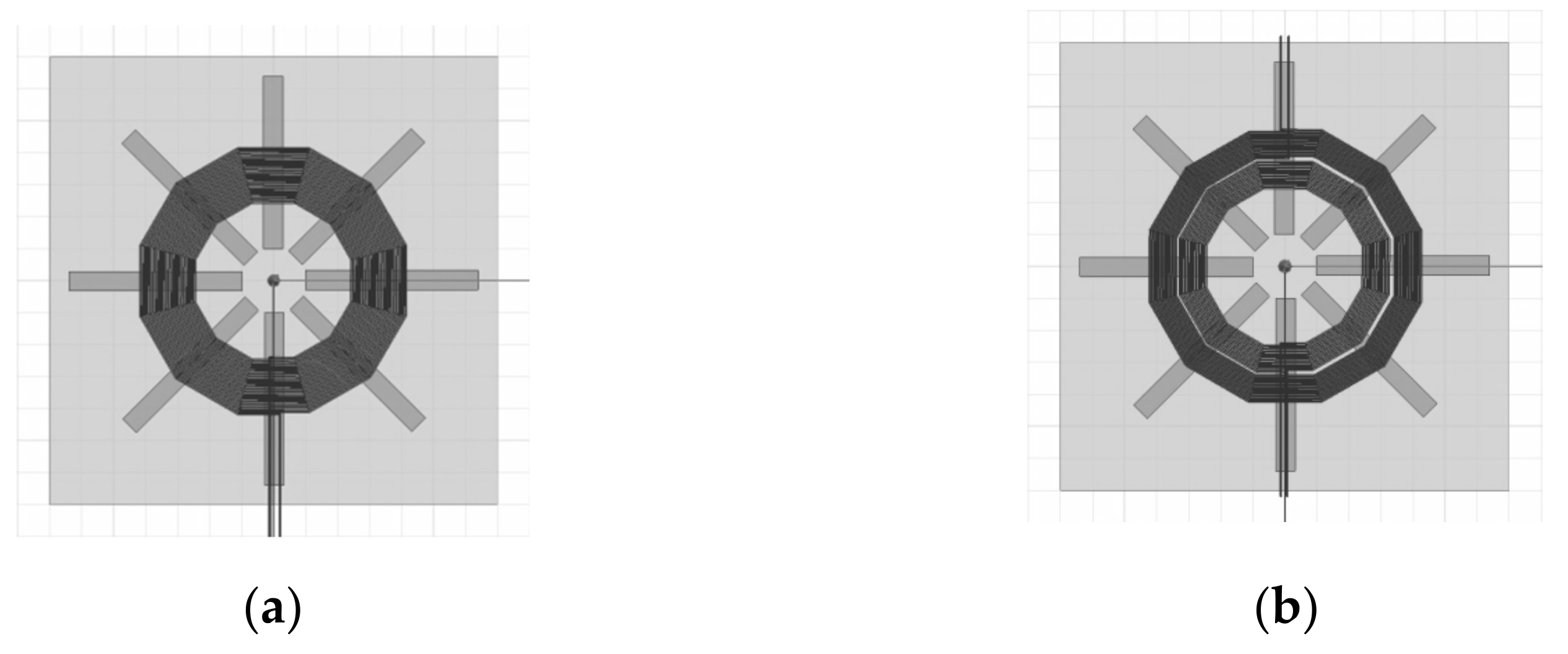
Another important aspect that needs to be addressed is the safety standards [19]. An aluminum shielding is required for the coils to isolate the large-field fluctuations from the exterior of the charging pad, even if the aluminum shielding decreases the quality factor of the system. A standard approach in dealing with this problem is to use ferrites, which minimize the flux affected by the shielding. The ferrites are placed below the coils, as shown in Figure 4, and the analysis of the ferrite bar arrangement is discussed in detail in [20]. Another factor that is taken into account by the proposed design is the high voltage on the series resonator’s Tx coil, which can reach up to tens of kV. A well-known solution to this problem is presented in [8,20], where the Tx coil is designed as two separate coils connected in parallel, thus reducing the total inductance. The two topologies (i.e., one single coil vs. two coils connected in parallel) are depicted in Figure 4.
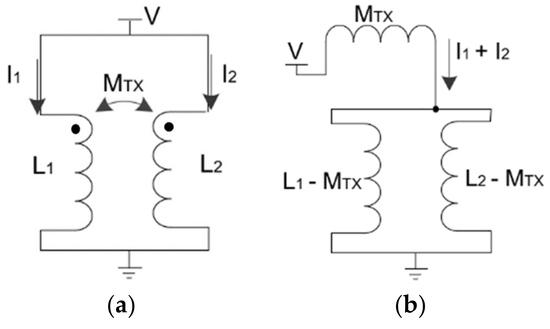
Figure 5a presents the electrical configuration, and Figure 5b presents the Z formalism network equivalent. and are the currents through the inner and exterior coils of the Tx, respectively.
is the mutual coupling between the inner Tx coil and the outer Tx coil. The total inductance of the parallel in-phase coupled coils is given by:
Based on the analysis and experimental results obtained in the prior work presented in [21], the diameter of the inner coil was determined to be , such that the entire coil assembly covers 30% to 60% of the ferrites’ length. The number of turns must be chosen so that the magnetic field in the center of the coil is maximized when supplied by a constant voltage source. The well-known empirical approximation of Harold A. Wheeler for the inductance of a spiral coil [22] is used:
where N is the number of turns and represents an average radius of the coil:
where represents the spacing between the centers of the wires of two adjacent turns. Equations (10) and (11) require that all values be expressed in inches. The currents passing through each inductor, as shown in Figure 5, can be calculated again with the help of the Z formalism:
In order to optimize the power transfer with respect to the number of turns of each of the two Tx coils, information on the variation of the coupling factor is needed. For that, electromagnetic simulations were performed, which served as an input for the following analysis. A finite element method (FEM) electromagnetic solver was used for simulation purposes. Once coupling information was obtained from FEM simulations, numerical simulations were carried out using Equations (12)–(14) to optimize the number of turns required in each coil.
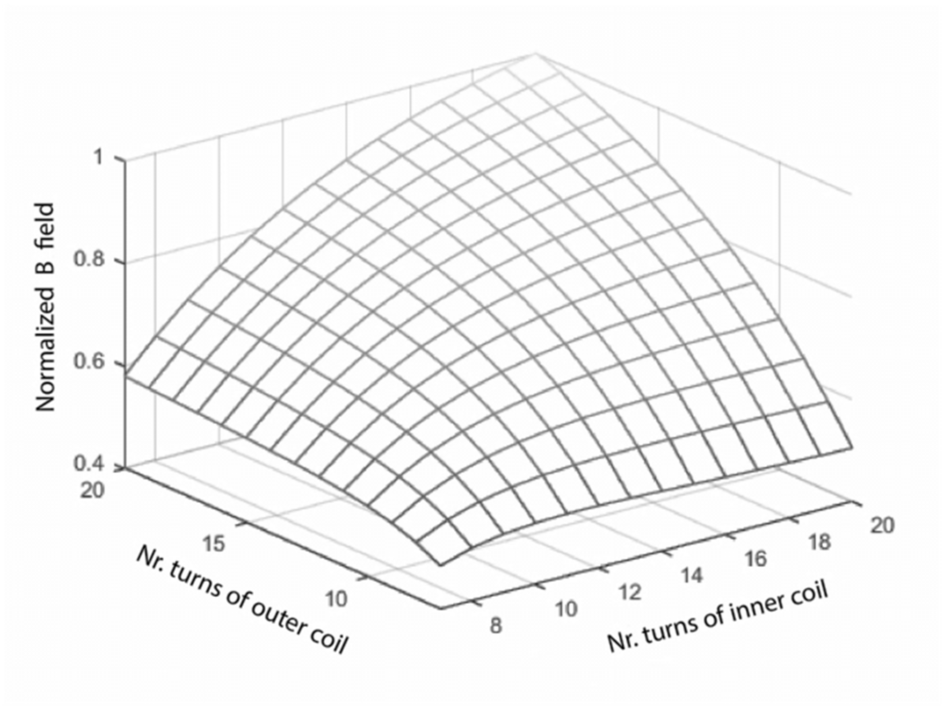
The composite B field at the center of the coil, presented in Figure 6, is given by the sum of two elements: the magnetic fields generated by through turns with an average radius of , and the magnetic field generated by through turns with an average radius of . The ferrite core plays an important role when estimating the currents and , as the arrangement and material of the cores will affect the value of both the mutual inductance and self-inductance. For simplicity, we have ignored the effect of the ferrite bars on the self-inductance, as it only affects the scale of the distribution, and not the shape.
The average radius was computed in terms of the distance between two adjacent wires, , such that for every additional turn, the radius is increased by . Varying the number of turns also changes the impedance of the coil and, therefore, the input power of the system. During all simulations, the input voltage was maintained constant because the proposed inverter, which is presented in the next section, is modeled as a constant voltage source. There are two normalizations applied to the quantity plotted in Figure 6 and described in Equation (14). The first one is different for each configuration and the field is normalized by the input power (which depends on the currents and inductances). The second normalization is a simple scaling with respect to the largest value presented in Figure 6, such that after normalization, the peak is at 0 dB. The normalization was performed since the only quantity of interest was the shape (distribution) and not the absolute values.
3.2. Rx Charging Pad Analysis
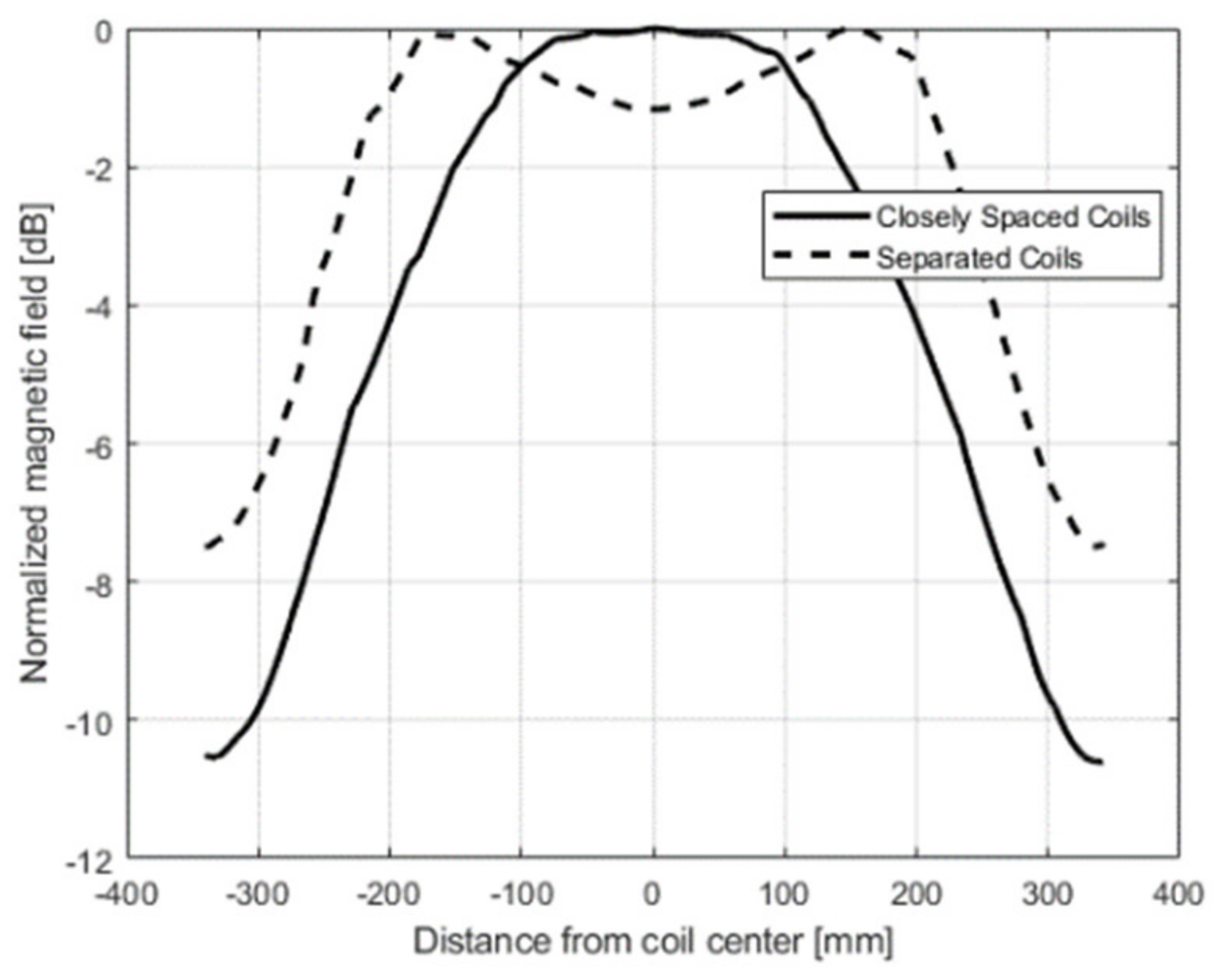
For the receiver design, all cost, aerodynamics, and weight limitations were considered. This leads to less turns used for the coil and elimination of ferrite bars. Moreover, a large inductance is highly undesired at the receiver end, as it may produce very high voltages. Using capacitors and transistors to step down the voltage can be rather expensive, and the voltage isolation will increase the weight of the UAV. This problem is solved similarly to the Tx system, and thus the Rx coil is designed from two concentrical, co-planar coils of different sizes and connected electrically in parallel. Unlike the Tx, where the outer coil and inner coil have similar diameters, the values of the two diameters are significantly different for the Rx coil. The FEM simulations presented in Figure 7 were performed for a constant height of 10 cm across the Rx coil. By using a larger coil, the Rx pad is less sensitive to positioning errors, while the smaller inner coil is key for high-power transfers. An important design specification is that the diameter of the outer coil of the Rx should match the diameter of the outer coil of the Tx for an optimal power transfer to size ratio.
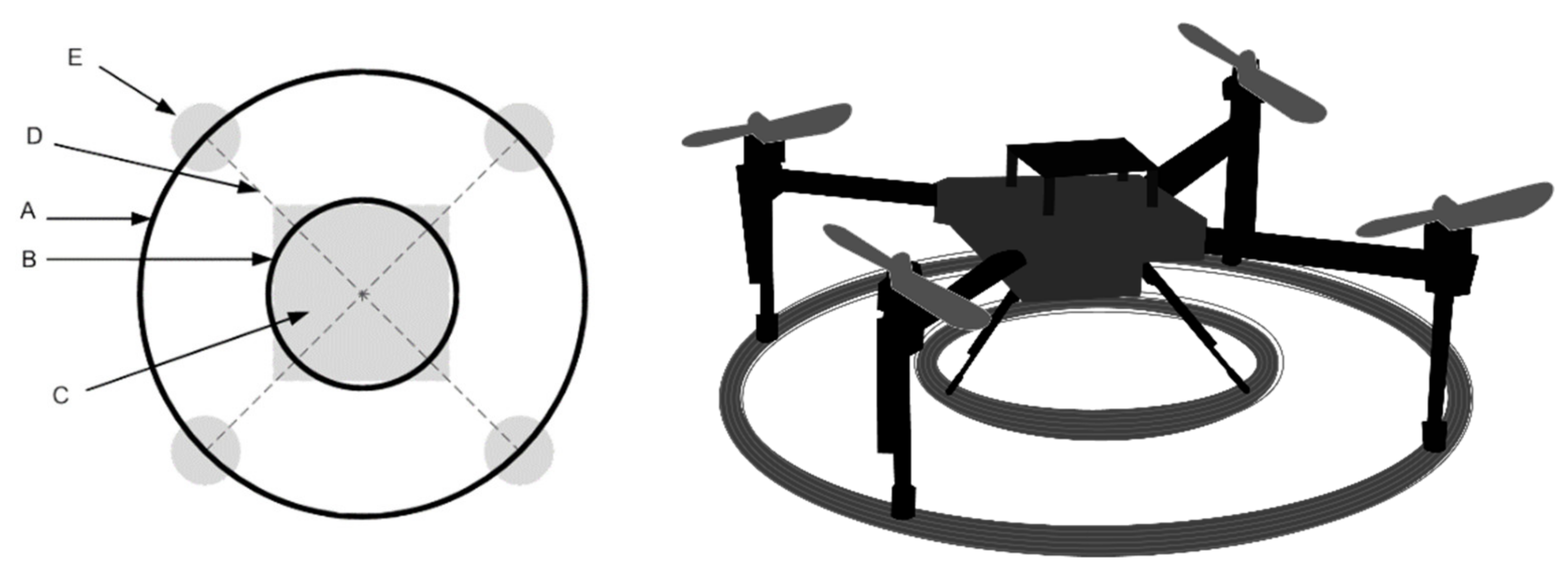
A possible optimization method for the size of the inner Rx coil is detailed in [23]. The referenced method is based on a priori statistical information on the distribution of the misalignment of the UAV. It further makes use of confidence intervals to optimize the geometry for maximum efficiency. The novelty of the design in the present paper is given by using a small inner coil inside a significantly larger outer coil for optimal weight distribution, power transfer, and misalignment tolerance. The turn/radius ratio of the interior/exterior coils is set to produce equal inductance on the two coils.
Figure 8 presents an aerodynamic and weight-efficient layout example of the Rx charging pad placed on a 4-rotor UAV chassis. The dimensions of the coils are determined as follows: As a first step, the exterior Rx coil’s radius is chosen so it may be placed below the UAV rotors. The interior coil should be attached to the body of the UAV. The number of turns for each coil is chosen such that their inductance is equal. The external Rx coil should also not exceed the diameter of the Tx coil.
3.3. Design Specifications of the Charging Pad
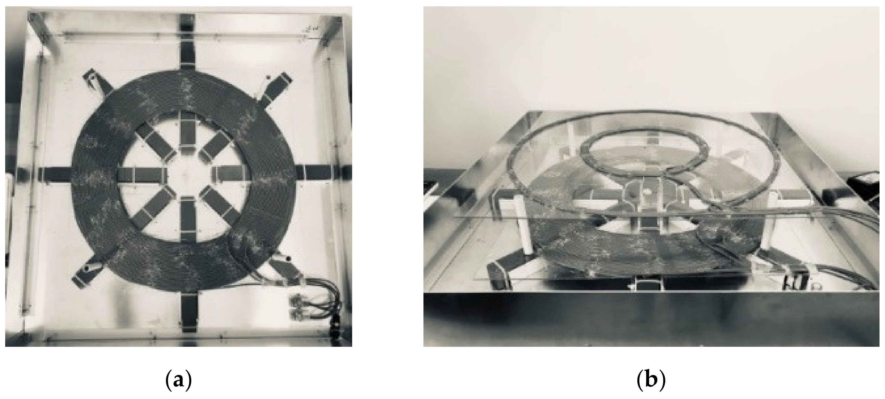
Both Tx and Rx coils have been designed with the same type of Litz wire, having a copper diameter of 1.6 mm and a copper + isolation diameter of 4 mm. The turn spacing was made as tight as possible. The 8 ferrite bars used were of type N87, with dimensions of 279 × 30 × 27 . The aluminum bottom shielding used was 70 × 70 , and the walls have a 10 cm height. The thickness of the aluminum shield is 2 mm. The parallel configuration of the two Tx coils is shown in Figure 9a, and the Tx–Rx configuration is shown in Figure 9b. Table 1 presents the Tx and Rx pad specifications.
4. Power Inverter Stage
In order to achieve a high efficiency, a switching class amplifier was used to convert the voltage from the DC power supply to AC current. An ideal Class-E amplifier can be modeled as a switch having a zero voltage drop when conducting and passing zero current when off [24]. Usually in WPT systems, the most common configuration used for the high-power DC–AC conversion is the H bridge configuration [25,26]. Typical H bridge designs use a dual-rail power supply, meaning the total number of batteries must be doubled. Thus, it is not a feasible solution for deployable systems. Another downside is that the output power is generally changed by modifying the gate voltage of the MOSFET transistors, which would require a specific set of transistors or to use PWM [27]. However, PWM would require a modulating signal of approximately 500 kHz, which is very impractical in high-power–high-current systems due to the extreme difficulty of phase matching the high-side and low-side transistors. Hitherto, the issue is that the current to voltage ratio for a given output power cannot be easily and robustly controlled by using an H bridge in this particular application.
An alternative and more efficient approach to H bridges is to use single-ended Class-E amplifiers, which are analyzed and presented in detail in [28]. However, these designs lack output power flexibility once the system has been implemented, and are highly influenced by changes of the load impedance.
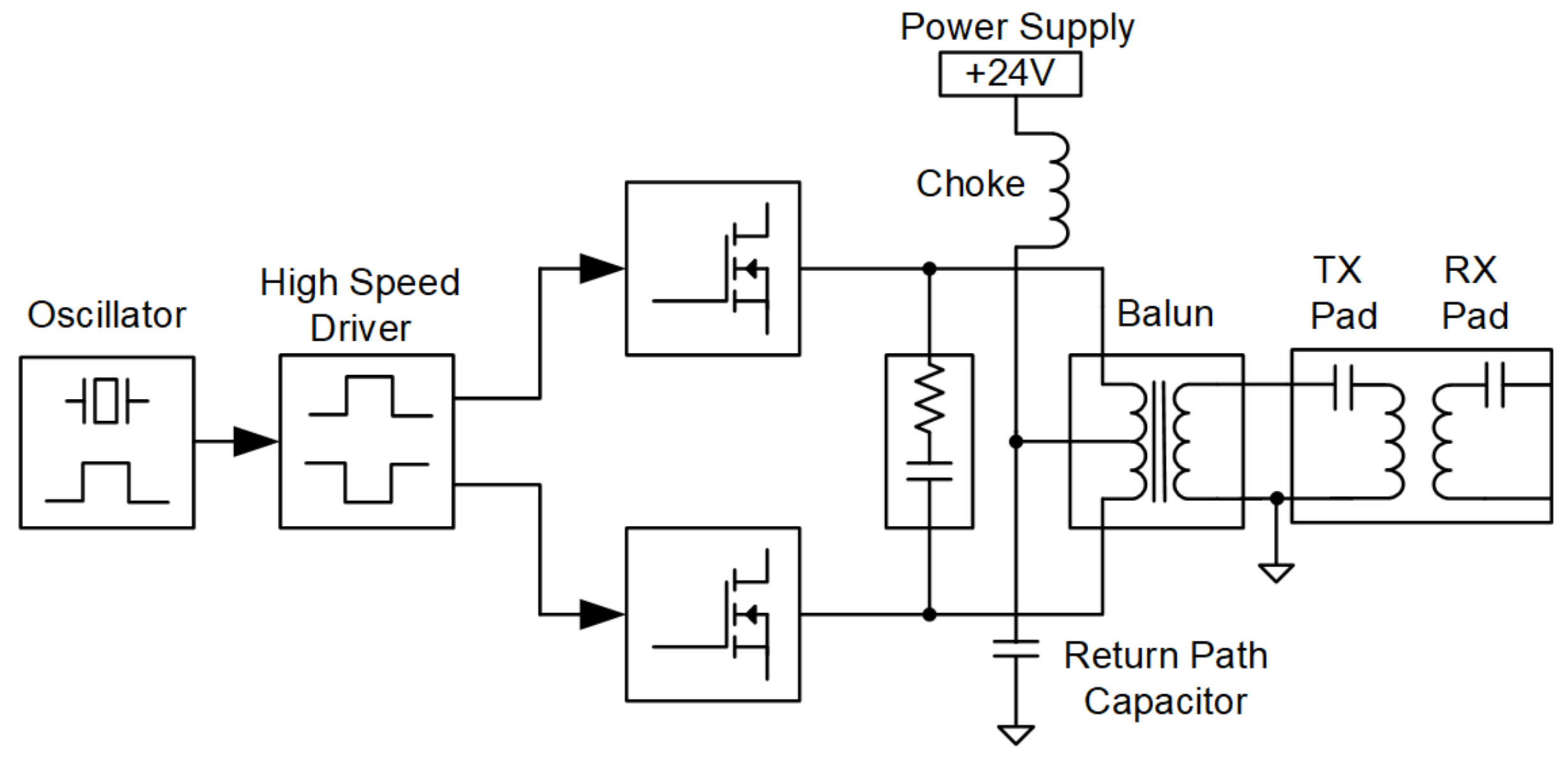
The design proposed in this paper has a higher theoretical efficiency than H bridges, and although it cannot offer the same large power transfers, very few UAVs require over 500 W of instantaneous power. The proposed design for the DC–AC inverter consists of two Class-E amplifiers in a dual-channel configuration, which are matched to the LC compensation network [29] via a transformer-based balun built on a ferrite torus. Figure 10 presents the circuit schematic of the proposed design. The major benefits of the design are that it runs on a single-rail power supply and that higher order compensation networks, such as those in [30,31], are not required, since impedance matching is carried out by changing the turn ratio of the balun transformer.
Furthermore, the four power MOSFETs (two in parallel for each phase) are operating in Class-E, either fully ON or fully OFF, thus dissipating very little power and requiring only a relatively small heat sink. Nonetheless, they must be kept reasonably cool, as their internal resistance ( (ON)) rises with temperature. It is experimentally shown that this approach works well at relatively low-supply DC voltage (+24 V), providing both high output power and high efficiency. Typical WPT systems used in EV charging that match the present system’s efficiency work at higher DC supply voltages (50 up to 300 V).
The Class-E amplifiers are driven by the high-speed driver MCP14E9 through parallel resistor/diode networks which slow the gate turn ON and speed up the gate turn OFF. This provides additional OFF time between the phase transitions, helps prevent cross-conduction, and provides some isolation between the two gates of the transistors that are placed in parallel. The transistors used in the present prototype are IRFP4227 MOSFETs with a nominal 25 mΩ rds-on resistance. The high-voltage transistors were used for safety and reliability purposes, at the cost of a lower efficiency. The Zobel configuration connected between the two channels plays a key role in eliminating ringing effects and high-voltage peaks that appear on the MOSFET transistors, caused by switching transients, parasitic resonances, and reflected waves. Simulations performed with a Spice simulator were carried out to ensure that no voltages throughout the entire system surpassed 800 V, which represents the breakdown voltage of the wire isolation used. The balun uses two 77 Mn-Zn ferrite toroids from Fair-Rite, with dimensions of 73 × 38 × 24 mm, and was designed for optimal power transfer.
Single-ended Class-E amplifiers have a return current capacitor connected between the Drain and Source of each MOSFET. In the present design, the Drain–Source capacitors are only used to filter ringing effects, together with the Zobel network, while the return path capacitor is placed between the power supply’s choke inductor and ground, right before the balun, as visible in Figure 10. Using the same return capacitor for both the high-side and low-side results in a better balancing, but will slightly decrease the system efficiency due to the additional copper and core losses in the balun. Since magnetic field distribution is a priority in the design of the Tx and Rx coils, the electric impedance matching must be performed by tuning the Zobel network and turning ratio of the balun.
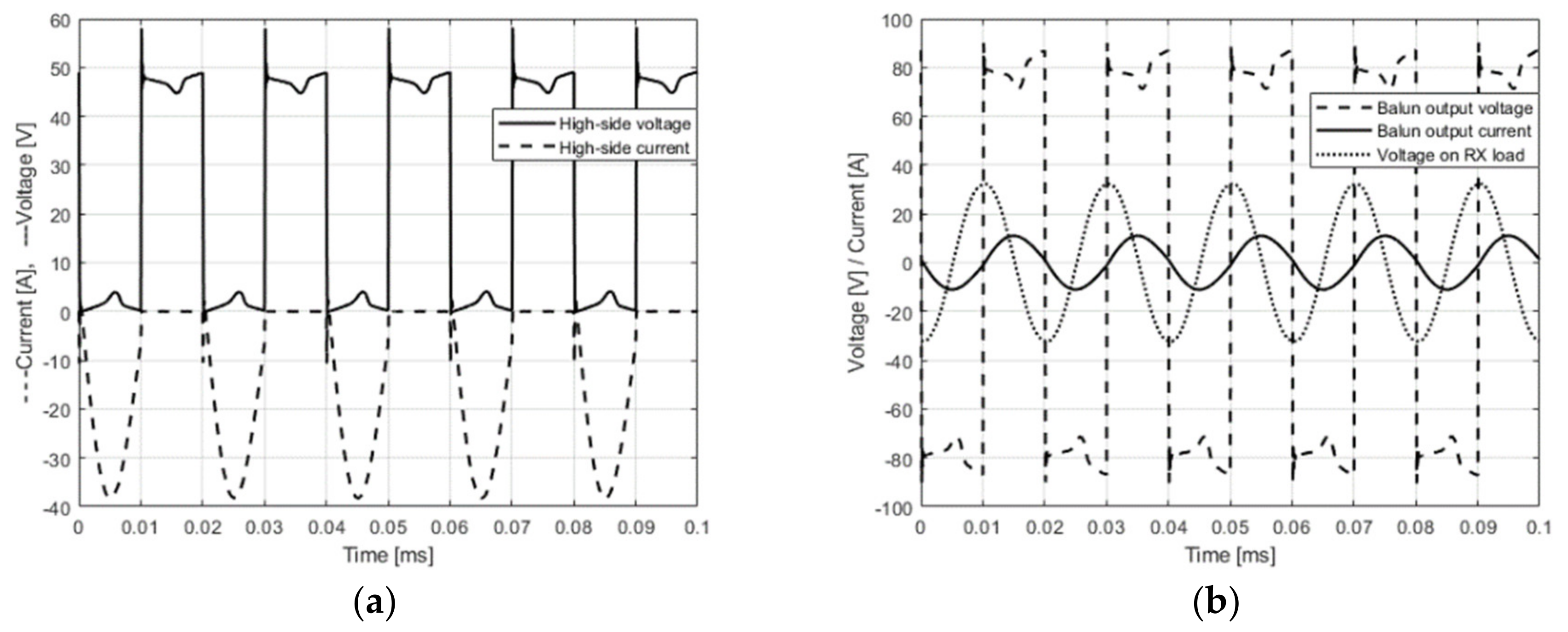
As mentioned, the high efficiency of the Class-E amplifier is due to the fact that when the MOSFETs are OFF, the theoretical conduction current is 0, and when the MOSFETs are ON, the theoretical voltage is 0. The zero-voltage switching (ZVS) and zero-voltage derivative switching (ZVDS) conditions for the proposed design are obtained by solving:
where is the driving pulse repetition interval, , is the high-side voltage, and is the low-side voltage. Figure 11a shows the simulated results of the waveforms in the drain of the MOSFET transistors from the high-side Class-E amplifier. The low-side channel waveforms are identical, but time-shifted by 180 degrees. In Figure 11b, simulated waveforms are shown for the signals obtained at the balun transformer secondary windings and the 1 Ω resistive load respectively, when the system is operating at 50 kHz. The signal fed into the Tx pad and the signal at the resistive load are out of phase by 90 degrees, which is consistent with the results obtained in Equations (3) and (4). By varying the number of turns in the secondary winding, the system can be tuned for better efficiency or for maximum power transfer, thus having the possibility to obtain an optimal compromise. The Class-E amplifiers were placed directly on a heavy aluminum heat sink for maximum heat dissipation. The control and protection system were placed on a FR-4 PCB at 1 cm above the heat sink. An RF choke and the large electrolytic capacitor are used to filter voltage and current ripples on the supply line.
5. Experimental Results
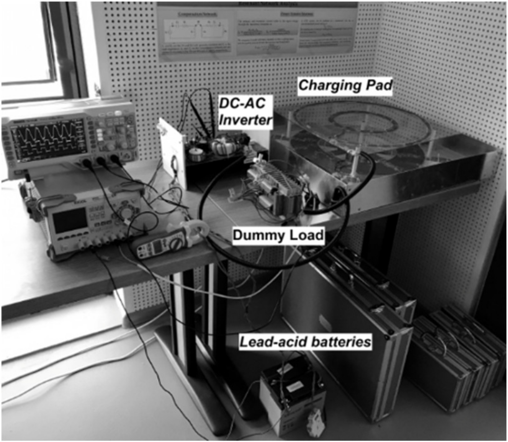
In this section, we first present the influence of the load impedance and positioning on the output power and the efficiency of the prototype. Load impedance changes are mainly caused by two factors: positioning errors of the UAV and the different charging stages of a Li-ion battery [32]. For the present prototype, shown in Figure 12, two series-connected 12 V/18 Ah lead-acid batteries were used to power the system in order to minimize supply broom noise and switching noises in the measurements. In all experiments, the load at the receiver’s end was dissipative and was made out of high-power resistors. Changing the configuration in which the resistors were placed made varying the load impedance very easy and precise. When transferring maximum power, the DC supply voltage dropped to about 22 V. The overall balancing of the power transfer and efficiency can be performed considering three factors: (a) the load impedance, (b) the coupling factor, which is provided by the distance between the Tx and Rx coils, and (c) the turn ratio of the balun transformer.
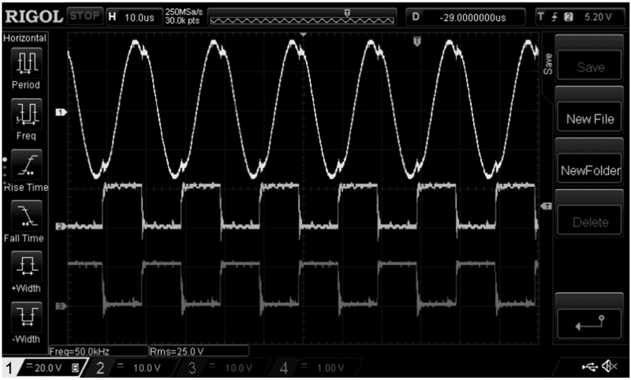
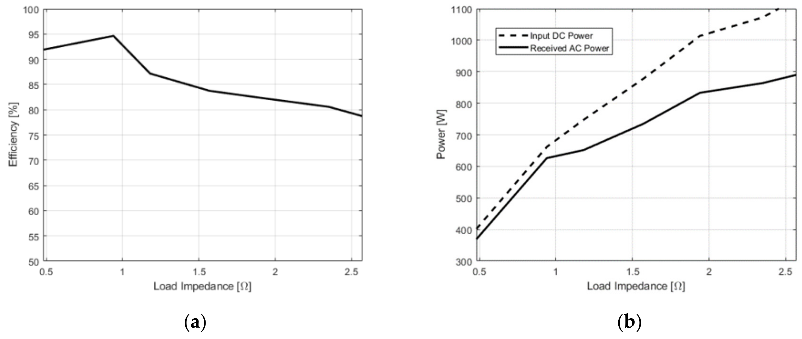
Since for a given UAV the charging distance is generally imposed, this leaves two degrees of freedom which can be used to optimize efficiency. The maximum system efficiency obtained is approximately 95%, which corresponds to an output power of 625 W and an input power of 660 W. The result was obtained when the Rx coil was placed 10 cm above the Tx pad and the load was set to 1 Ω. System efficiency is calculated as the ratio between the input DC power and the output AC power. The final AC–DC converter block is not taken into consideration since it is not within the scope of this paper, but a compatible design example can be found in [33]. The input power of the DC–AC inverter was calculated as the DC battery voltage multiplied by the current, both measured with a true RMS clamp meter, and by measuring the voltage across a high-power shunt resistor. The output power of the system was calculated as the squared RMS voltage drop on the load divided by the load’s impedance. The voltage waveform obtained at the load was a 25 sinusoid 90 degrees out-of-phase, relative to the driving square wave voltage, as depicted in Figure 13. The result is consistent with both theory and the Spice simulations. The distortion seen in the load voltage waveform in Figure 13 is caused by the additional inductance of the wiring used to connect the load resistors together. Our tests and simulations have shown that this distortion was small and had a negligible effect on system efficiency.
The efficiency and input/output power that were obtained are presented in Figure 14a,b respectively, when the load impedance was varied between 0.5 and 2.5 Ω. Comparing the obtained system efficiency results shown in Figure 14a and the simulated transfer efficiency from Figure 3, it can be inferred that the PA reached a peak efficiency of 98%.
When increasing the vertical distance between the Tx and Rx coils up to a certain point of approximately 20 cm, the transferred power will continue to increase. This can be explained by revising the analysis performed in Section 2.2., more precisely Equations (3) and (4), which state that if the system is weakly coupled, the Tx current increases, giving rise to large magnetic fields. Evidently, this increased power transfer comes at the cost of a lower efficiency. The obtained experimental results are shown in Table 2.
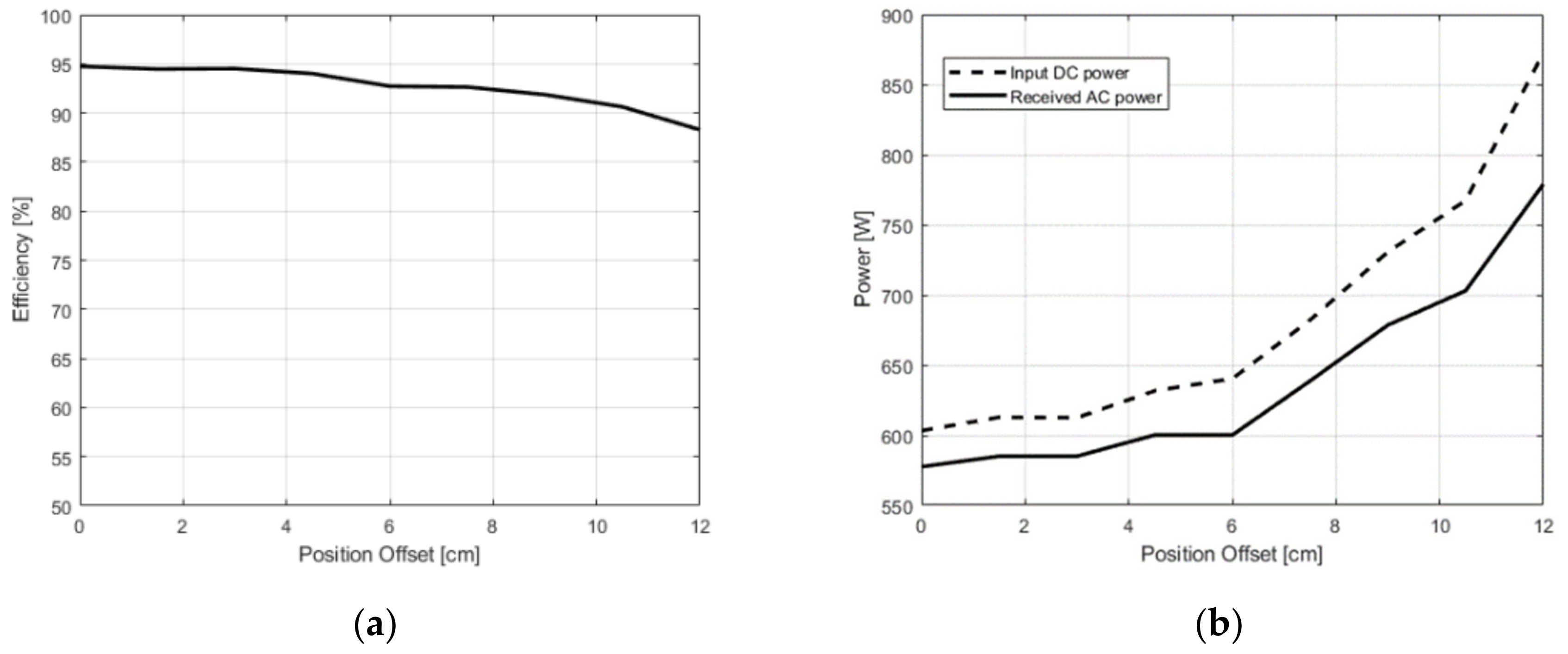
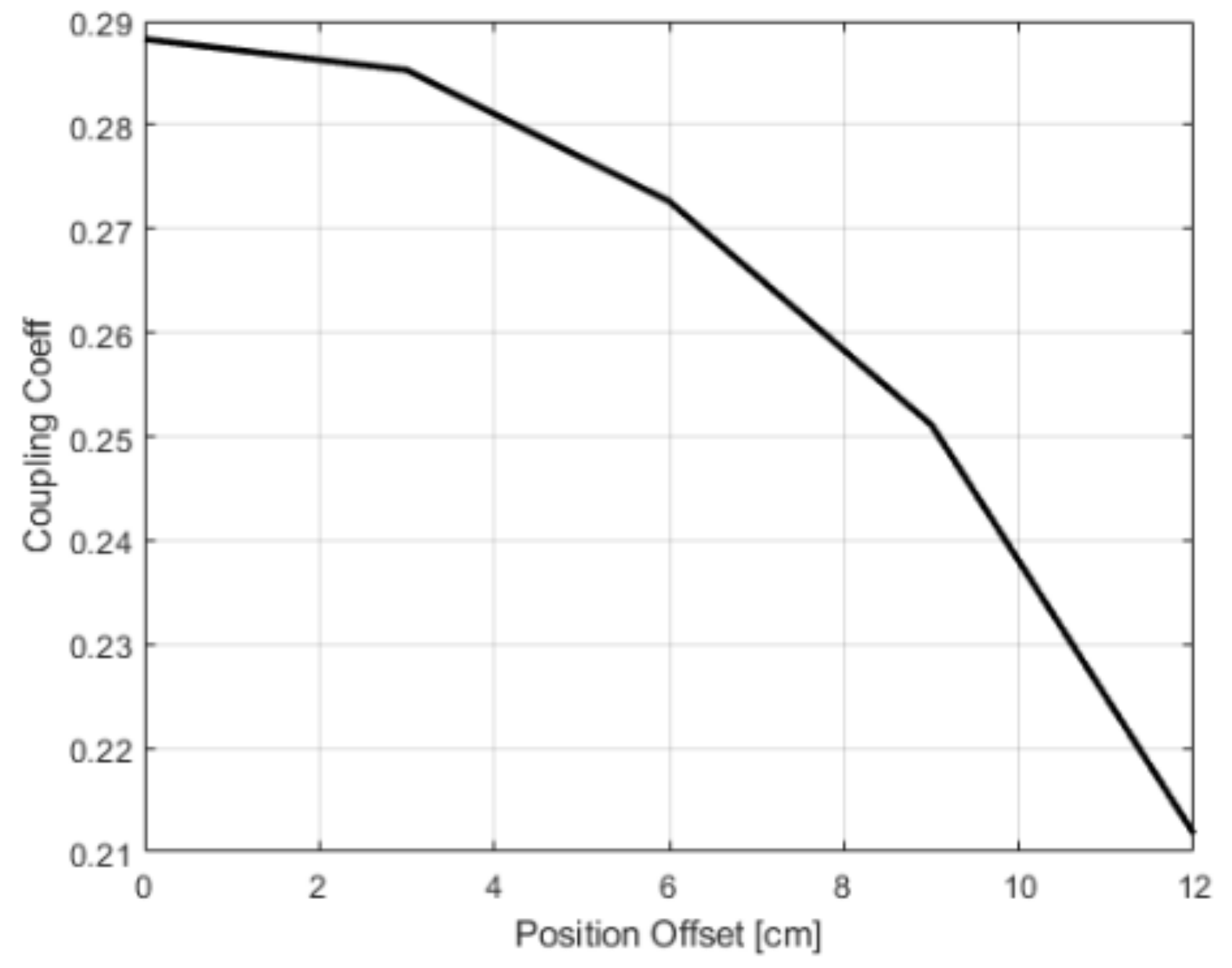
A similar result was achieved for horizontal offset, caused by positioning errors of the UAV. Figure 15a,b graphically present the efficiency and the input/output power respectively, as a function of horizontal positioning offset between the two center points of the Tx pad and the Rx pad. The magnetic coupling between the Tx and Rx coils is presented in Figure 16. All horizontal offset measurements were performed at a constant height of 10 cm. By comparing the results in Table 2 and Figure 16, it can be seen that the coupling is much less sensitive to horizontal offsets than it is to vertical offsets. This is mainly due to the wide and flat horizontal field distribution of the Tx pad. Moreover, when Equation (8) is satisfied, and when the copper and core losses are very small, variations in coupling below a certain threshold have little effect on efficiency.
6. Conclusions
In this paper, a highly efficient VLF WPT charging system used for fast-charging large UAVs was presented. The proposed DC–AC inverter is based on a modified Class-E amplifier. The advantages of this solution are summarized in Table 3.
The presented design showed promising opportunities and results, from both simulations and experimental results. A new Rx coil geometry was proposed which was designed such that it offers a sweet spot when choosing between maximum power transfer, efficiency, weight, and receiver cost. A peak system efficiency of 95% was obtained at 10 cm, with a power transfer of 625 W. Compared to previously mentioned designs, the present system offers the capability of similar performance but without the need of a dual-rail supply, complex matching networks, or ferrite bars at the receiver’s end. A comparison with other work was presented in Table 3. However, please note that high-power transfers (as in [12,26,32]) can only be achieved in EV applications that do not have weight constraints. Such solutions are impossible to implement in a light UAVs with similar efficiencies.
Given the simplistic low-voltage supply requirements and the relatively reduced weight and size, the system makes an excellent candidate for a mobile deployment system for industrial and defense UAV charging applications.
Author Contributions
The research and development of the proposed Wireless Power Transfer system for UAV applications, consisting of the DC-AC inverter and the Tx-Rx pads, F.R.; The presented prototype was optimized using mathematical derivations, Spice simulations, Numerical simulations, FEM simulations and multiple experiments, A.B.; All authors have read and agreed to the published version of the manuscript.
Funding
This work was supported by a grant of the Romanian Ministry of Research and Innovation, CCCDI—UEFISCDI, project number: “PN-III-P1-1.2-PCCDI-2017 0839/19PCCDI ⁄ 2018, within PNCDI III”.
Conflicts of Interest
The authors declare no conflict of interest.
References
- Sullivan, J.M. Evolution or revolution? The rise of UAVs. IEEE Technol. Soc. Mag. 2006, 25, 43–49. [Google Scholar] [CrossRef]
- Qazi, S.; Siddiqui, A.S.; Wagen, A.I. UAV based real time video surveillance over 4G LTE. In Proceedings of the Conference on Open Source Systems and Technologies (ICOSST), Lahore, Pakistan, 17–19 December 2015; pp. 141–145. [Google Scholar]
- Mahardika, M.; Nugroho, G.; Prasetyo, E.Y. UAV long range surveillance system based on BiQuad antenna for the Ground Control Station. In Proceedings of the IEEE Student Conference on Research and Development (SCOReD), Kuala Lumpur, Malaysia, 13–14 December 2016; pp. 1–5. [Google Scholar]
- Stacy, N.J.S.; Craig, D.W.; Staromlynska, J.; Smith, R.B. The Global Hawk UAV Australian deployment: Imaging radar sensor modifications and employment for maritime surveillance. In Proceedings of the IEEE International Geoscience and Remote Sensing Symposium, Toronto, ON, Canada, 24–28 June 2002. [Google Scholar]
- Turner, D.; Lucieer, A.; Wallace, L. Direct Georeferencing of Ultrahigh-Resolution UAV Imagery. IEEE Trans. Geosci. Remote Sens. 2014, 52, 2738–2745. [Google Scholar] [CrossRef]
- Lort, M.; Aguasca, A.; Lopez-Martinez, C.; Marin, T.M. Initial Evaluation of SAR capabilities in UAV Multicopter Platforms. IEEE J. Sel. Top. Appl. Earth Obs. Remote Sens. 2018, 11, 127–140. [Google Scholar] [CrossRef] [Green Version]
- Sharma, V.; Kumar, R.; Rana, P.S. Self-Healing Neural Model for Stabilization against Failures over Networked UAVs. IEEE Commun. Lett. 2015, 19, 2013–2016. [Google Scholar] [CrossRef]
- Covic, G.A.; Boys, J.T. Modern Trends in Inductive Power Transfer for Transportation Applications. IEEE J. Emerg. Elect. Top. Power Electron. 2014, 1, 28–41. [Google Scholar] [CrossRef]
- Samad, T.; Bay, J.S.; Godbole, D. Network-Centric Systems for Military Operations in Urban Terrain: The Role of UAVs. Proc. IEEE 2007, 95, 92–107. [Google Scholar] [CrossRef]
- Li, K.; Voicu, R.C.; Kanhere, S.S.; Ni, W.; Tovar, E. Energy Efficient Legitimate Wireless Surveillance of UAV Communications. IEEE Trans. Veh. Technol. 2019, 68, 2283–2293. [Google Scholar] [CrossRef]
- Rosu, F.; Badescu, A.; Rusu, B. Analysis and Optimization of an IPT System. In Proceedings of the SPIE Conference ATOM-N, Constanta, Romania, 23–26 August 2018. [Google Scholar]
- Lu, F.; Zhang, H.; Kan, T.; Hoffmann, H.; Mei, Y.; Cai, L.; Mi, C. A high efficiency and compact inductive power transfer system compatible with both 3.3 kW and 7.7 kW receivers. In Proceedings of the IEEE Applied Power Electronics Conference and Exposition (APEC), Tampa, FL, USA, 26–30 March 2017; pp. 3669–3673. [Google Scholar]
- Covic, G.A.; Boys, J.T. Inductive Power Transfer. Proc. IEEE 2013, 101, 1276–1289. [Google Scholar] [CrossRef]
- Ohira, T. What in the world is Q? IEEE Microw. Mag. 2016, 17, 42–49. [Google Scholar] [CrossRef]
- Musavi, F.; Eberle, W. Overview of wireless power transfer technologies for electric vehicle battery charging. IET Power Electron. 2014, 7, 60–66. [Google Scholar] [CrossRef]
- Poon, A.S.Y. A General Solution to Wireless Power Transfer between Two Circular Loop. Prog. Electromagn. Res. 2014, 148, 171–182. [Google Scholar] [CrossRef] [Green Version]
- Aditya, K.; Williamson, S.S. Comparative study of series-series and series-parallel topology for long track EV charging application. In Proceedings of the IEEE Transportation Electrification Conference and Expo (ITEC), Dearborn, MI, USA, 15–18 June 2014; pp. 1–5. [Google Scholar]
- Sallan, J.; Villa, J.L.; Llombart, A.; Sanz, J.F. Optimal Design of ICPT Systems Applied to Electric Vehicle Battery Charge. IEEE Trans. Ind. Electron. 2009, 56, 2140–2149. [Google Scholar] [CrossRef]
- ARPANSA. Maximum Exposure Levels to Radiofrequency Fields—3 kHz to 300 GHz; Australian Radiation Protection and Nuclear Safety Agency: Melbourne, Australia, 2002. [Google Scholar]
- Budhia, M.; Covic, G.A.; Boys, J.T. Design and optimization of Circular Magnetic Structures for Lumped Inductive Power Transfer Systems. IEEE Trans. Power Electron. 2011, 26, 3096–3108. [Google Scholar] [CrossRef]
- Rosu, F.; Badescu, A. Patent Pending, A/01188, Submitted in 2019. Available online: https://worldwide.espacenet.com/patent/search/family/068293301/publication/RO133690A0?q=Filip%20Rosu (accessed on 8 September 2021).
- Wheeler, H.A. Simple Inductance Formulas for Radio Coils. Proc. Inst. Radio Eng. 1928, 16, 1398–1400. [Google Scholar] [CrossRef]
- Sampath, J.P.K.; Alphones, A.; Vilathgamuwa, D.M. Coil optimization against misalignment for wireless power transfer. In Proceedings of the IEEE 2nd Annual Southern Power Electronics Conference (SPEC), Auckland, New Zealand, 5–8 December 2016; pp. 1–5. [Google Scholar]
- Hirayama, K.; Suetsugu, T.; Kurokawa, F. DC-DC converter based on voltage dividing class E amplifier. In Proceedings of the IEEE International Telecommunications Energy Conference, Broadbeach, Australia, 22–26 October 2017; pp. 535–540. [Google Scholar]
- Hao, H.; Covic, G.A.; Boys, J.T. A Parallel Topology for Inductive Power Transfer Power Supplies. IEEE Trans. Power Electron. 2014, 29, 1140–1151. [Google Scholar] [CrossRef]
- Chen, L.; Nagendra, G.R.; Boys, J.T.; Covic, G.A. Double-Coupled Systems for IPT Roadway Applications. IEEE J. Emerg. Sel. Top. Power Electron. 2015, 3, 37–49. [Google Scholar] [CrossRef]
- Tang, L.-C.; Jeng, S.-L.; Chang, E.-Y.; Chieng, W.-H. Variable-Frequency Pulse Width Modulation Circuits for Resonant Wireless Power Transfer. Energies 2021, 14, 3656. [Google Scholar] [CrossRef]
- Aldhaher, S.; Chi-Kwong Luk, P.; Bati, A.; Whildborne, J.F. Wireless Power Transfer Using Class E Inverter with Saturable DC-Feed Inductor. IEEE Trans. Ind. Appl. 2014, 50, 2710–2718. [Google Scholar] [CrossRef] [Green Version]
- Wang, Q.; Che, W.; Dionigi, M.; Mastri, F.; Mongiardo, M.; Monti, G. Gains Maximization via Impedance Matching Networks for Wireless Power Transfer. Prog. Electromagn. Res. 2019, 164, 135–153. [Google Scholar] [CrossRef] [Green Version]
- Borage, M.; Tiwari, S.; Kotaiah, S. Analysis and design of an LCL-T resonant converter as a constant-current power supply. IEEE Trans. Ind. Electron. 2005, 52, 1547–1554. [Google Scholar] [CrossRef]
- Pantic, Z.; Sanzhong, B.; Lukic, S. ZCS LCC-compensated resonant inverter for inductive-power-transfer application. IEEE Trans. Ind. Electron. 2011, 58, 3500–3510. [Google Scholar] [CrossRef]
- Vu, V.B.; Tran, D.H.; Choi, W. Implementation of the Constant Current and Constant Voltage Charge of Inductive Power Transfer Systems with the Double-SidedLCCCompensation Topology for Electric Vehicle Battery Charge Applications. IEEE Trans. Power Electron. 2018, 33, 7398–7410. [Google Scholar] [CrossRef] [Green Version]
- Tashakor, N.; Khooban, M. An Interleaved Bi-directional AC-DC Converter with Reduced Switches and Reactive Power Control. IEEE Trans. Circuits Syst. II Express Briefs 2020, 67, 132–136. [Google Scholar] [CrossRef]
Figure 1.
Schematic of an inductive WPT system.

Figure 2.
Series–series topology of the resonant WPT system.

Figure 3.
Transfer efficiency as a function of load impedance for , , and .

Figure 4.
(a) Single coil design. (b) Double coil design with two concentric coils electrically connected in parallel. A total of 8 ferrite bars are placed below the coils, in a radial configuration.
Figure 4.
(a) Single coil design. (b) Double coil design with two concentric coils electrically connected in parallel. A total of 8 ferrite bars are placed below the coils, in a radial configuration.

Figure 5.
(a) Electric configuration of the parallel connected Tx coils. (b) The Z formalism network equivalent.
Figure 5.
(a) Electric configuration of the parallel connected Tx coils. (b) The Z formalism network equivalent.

Figure 6.
Magnetic flux density, for a constant voltage input, at the center of the pad, as a function of (the inner coil number of turns) and (the exterior coil number of turns).
Figure 6.
Magnetic flux density, for a constant voltage input, at the center of the pad, as a function of (the inner coil number of turns) and (the exterior coil number of turns).

Figure 7.
Simulated magnetic field intensity of the Rx charging pad (finite element simulation) at a height of 10 cm. The dotted line represents the field distribution when the coils are designed such that both the inner and exterior coil are close together, and the continuous line represents the field distribution when there is a big difference between the inner diameters of the two coils.

Figure 8.
Positioning of the proposed Rx coil on the UAV chassis. “A” represents the outer Rx coil, “B” represents the inner Rx coil, “C” represents the UAV chassis, and “D” represents the “wings” of the UAV to which the motors represented by “E” are attached.
Figure 8.
Positioning of the proposed Rx coil on the UAV chassis. “A” represents the outer Rx coil, “B” represents the inner Rx coil, “C” represents the UAV chassis, and “D” represents the “wings” of the UAV to which the motors represented by “E” are attached.

Figure 9.
(a) The Tx pad. (b) The Tx–Rx pads.

Figure 10.
Block schematic of the proposed DC–AC inverter. The inverter is supplied via the balun transformer. ON/OFF switching generates a 50 kHz, 48 V square wave in the primary windings.
Figure 10.
Block schematic of the proposed DC–AC inverter. The inverter is supplied via the balun transformer. ON/OFF switching generates a 50 kHz, 48 V square wave in the primary windings.

Figure 11.
(a) Simulated results of the waveforms in the drain of the MOSFET transistors. The current is represented with a dashed line, and the voltage with a continuous line. (b) Simulated results of the input waveforms from the secondary winding of the balun T1 and the output voltage at the resistive load (RL). The voltage is represented with the dashed line, the current is represented with the continuous line, and the voltage received at the resistive load is represented with the dotted line.

Figure 12.
The proposed WPT system.

Figure 13.
Waveform 1 (top) represents the output voltage across the 1 Ω load, and waveforms 2 and 3 (bottom) represent the driving signals of the Class-E inverter. The 25 and 50 kHz readings are from waveform 1.
Figure 13.
Waveform 1 (top) represents the output voltage across the 1 Ω load, and waveforms 2 and 3 (bottom) represent the driving signals of the Class-E inverter. The 25 and 50 kHz readings are from waveform 1.

Figure 14.
(a) Measured DC to AC system efficiency as a function of load impedance, for a distance of 10 cm between the Rx and Tx, with a coupling factor of 0.29. (b) Measured input DC power (dashed line) and output AC power (continuous line).
Figure 14.
(a) Measured DC to AC system efficiency as a function of load impedance, for a distance of 10 cm between the Rx and Tx, with a coupling factor of 0.29. (b) Measured input DC power (dashed line) and output AC power (continuous line).

Figure 15.
(a) Measured DC to AC system efficiency as a function of horizontal displacement, for a load impedance of 1 Ω. (b) Measured input DC power (dashed line) and output AC power (continuous line).
Figure 15.
(a) Measured DC to AC system efficiency as a function of horizontal displacement, for a load impedance of 1 Ω. (b) Measured input DC power (dashed line) and output AC power (continuous line).

Figure 16.
Measured coupling coefficient between Tx and Rx coils as a function of horizontal position offset.
Figure 16.
Measured coupling coefficient between Tx and Rx coils as a function of horizontal position offset.


Table 1.
WPT charging pad specifications.
| Specifications | Tx Coil | Rx Coil | Units |
|---|---|---|---|
| Inner coil turns | 14 | 5 | turns |
| Outer coil turns | 14 | 3 | turns |
| Inner coil inner diameter | 300 | 210 | mm |
| Outer coil inner diameter | 400 | 475 | mm |
| Inner coil self-inductance | 172 | 13.5 | μH |
| Outer coil self-inductance | 218 | 13.8 | μH |
| Inner/Outer mutual inductance | 110 | 1.75 | μH |
| Parallel configuration inductance | 149 | 7.6 | μH |
| Parallel unloaded Q at 50 kHz | 200 | 80 | |
| Tx–Rx xoupling (k) at 10 cm | 0.29 | ||
Table 2.
Vertical offset measurements.
| Height (cm) | Coupling | Tx Power (W) | Rx Power (W) | Efficiency (%) |
|---|---|---|---|---|
| 10 | 0.29 | 660 | 625 | 94.7 |
| 20 | 0.11 | 1840 | 1142 | 62 |
Table 3.
Prior state-of-the-art system comparison.
| Ref. | Efficiency (%) | Output Power (W) | Frequency (kHz) | Supply Voltage (V) | Inverter Configuration | Charging Distance (cm) | Application |
|---|---|---|---|---|---|---|---|
| [12] | 95 | 900 | 85 | +360 | H-Brdige | 15 | EV |
| [32] | 96.1 | 6600 | 67.5 | +420 | H-Bridge | 20 | EV |
| [26] | 95 | 5000 | 20 | +600 | H-bridge | - | EV |
| [28] | 80 | 11.75 | 750 | +8 | Class-E PA | 1.25 | Low-Power |
| Proposed | 94 | 625 | 50 | +24 | Dual-Channel Class-E PA | 10 | UAV |
Publisher’s Note: MDPI stays neutral with regard to jurisdictional claims in published maps and institutional affiliations. |
© 2021 by the authors. Licensee MDPI, Basel, Switzerland. This article is an open access article distributed under the terms and conditions of the Creative Commons Attribution (CC BY) license (https://creativecommons.org/licenses/by/4.0/).
Share and Cite
MDPI and ACS Style
Rosu, F.; Badescu, A. Electric and Magnetic Design of a Deployable WPT System for Industrial and Defense UAV Applications. Electronics 2021, 10, 2252. https://doi.org/10.3390/electronics10182252
AMA Style
Rosu F, Badescu A. Electric and Magnetic Design of a Deployable WPT System for Industrial and Defense UAV Applications. Electronics. 2021; 10(18):2252. https://doi.org/10.3390/electronics10182252
Chicago/Turabian StyleRosu, Filip, and Alina Badescu. 2021. "Electric and Magnetic Design of a Deployable WPT System for Industrial and Defense UAV Applications" Electronics 10, no. 18: 2252. https://doi.org/10.3390/electronics10182252
Note that from the first issue of 2016, this journal uses article numbers instead of page numbers. See further details here.