
Abstract
In the last few decades, increasing research effort has focused on the design of telecommunication payload systems with advanced features and lower costs in space applications. In this context, photonic solutions have already proven the potential to achieve additional functionalities, such as multiplexing or switching of RF or microwave signals, with consequent additional benefits in terms of size and mass reduction. In this paper, we report on the design of a 2 × 2 switching cell based on a thermo-optic interferometric configuration, whose key element is a sub-wavelength grating. We have theoretically demonstrated a broadband operation, with better performance in terms of operating wavelength range and compactness with respect to the existing interferometric cells. The switching cell shows a worst extinction ratio of about 13 dB, insertion loss of less than 2 dB, crosstalk of 12 dB, over a bandwidth of 150 nm, within a footprint as small as 240 µm × 9 µm. To demonstrate its potential use as a routing fabric in flexible telecommunication satellite payloads, as an example, the designed switching cell has been used as a building block of an 8 × 8 dilated Banyan matrix, where large bandwidth (150 nm), low crosstalk (−38 dB), small footprint (≈1620 µm × 576 µm) and relatively low power consumption (276 mW) have been achieved.
Export citation and abstract BibTeX RIS

Original content from this work may be used under the terms of the Creative Commons Attribution 4.0 license. Any further distribution of this work must maintain attribution to the author(s) and the title of the work, journal citation and DOI.
1. Introduction
The evolution of optical transport networks over recent decades, in supporting the ever-increasing demand for coverage, capacity and flexibility, has seen photonic switches as key elements for essential functions, such as protection, signal monitoring, cross-connection and add-drop multiplexing [1–3]. This is due to their performance in terms of bandwidth, power consumption, switching time, high-level integration and compactness. These characteristics, together with the potential of realizing reconfigurable, programmable and scalable switching fabrics make photonic switches promising candidates for applications in data centres, cloud servers and high-throughput computing [4–6].
Due to the strong interest in their applicability in flexible telecommunication networks, several switching technologies have been intensively investigated, including Micro Electro-Mechanical Systems (MEMS) switching matrices [7, 8], LiNbO3-based switches [9, 10], III–IV-based switches [11, 12], semiconductor optical amplifier switching matrices [13, 14], liquid crystal-based switches [15, 16], all-optical switches [17, 18], etc. Different configurations, exploiting several physical effects, operating principles and/or geometrical configurations have been proposed. Some of these technologies, such as liquid crystal, magneto-optic, bulk electro-optic and waveguide electro-optic have also achieved good market success. In this regard, they are providing flexibility in optical network connectivity, including optical protection, fibre test systems, remotely reconfigurable multiplexers and sensing [19, 20]. Several topologies can be considered for connecting basic switching cells with the aim of realizing large N × N switching matrices [21]. From a technology standpoint, several challenges need to be addressed, such as scalability, loss, speed and cost. In particular, in the Telecommunication (TLC) domain, users demand to scale to several thousand ports to route a large number of optical signals. In order to avoid the blocking behaviour of a large switching matrix, scalable switching configurations, made of non-blocking elements, are required, with high reliability and low cost. The features of a single non-blocking element, such as the number of input/output ports, extinction ratio, crosstalk and insertion loss should be taken into account to predict the performance of a scalable switching matrix. Finally, the power link and optical signal-to-noise ratio budgets of the switching matrix should also be addressed, with the aim of increasing the optical switching matrix attractiveness and paving the way for the exploitation of multi-stage architectures.
More recently, studies have been carried out on the potential of photonic switching technologies in Space, where they can find applications in Laser Detection and Ranging (LIDAR), altimeters, sensing systems, communication terminals and on-board communication architectures. When evaluating the switching technology more appropriately for Space, specific attention must be paid to some features, such as switching speed, insertion loss, crosstalk, scalability, multiplexing capability and reliability. As an example, there should be more than two input/output ports, a response time in the order of a few µs, an insertion loss of less than 3 dB and crosstalk lower than −20 dB in a TLC payload [19, 20].
Early investigations were focused mainly on MEMS technology for large switching matrices in TLC payloads [7, 22–25]. MEMS optical switching matrices show low insertion loss (in the order of a few dB) and ultra-low crosstalk (<−50 dB), but at the expense of switching times in the order of ms, large power consumption (in the order of W) and very large footprint (in the order of mm2). More recently, interest has turned to more reliable switching configurations with no moving parts for solutions, such as integrated microphotonic switching, already largely investigated for terrestrial applications and available in the market. Analyses have been proposed on the challenges and benefits of adapting commercial off-the-shelf solutions to Space applications, demonstrating crosstalk <−20 dB, switching time <500 µs, port number >2, power consumption in the order of hundreds of mW, and footprints in the order of hundreds of mm2 [19, 20].
Emerging applications in the space industry are increasingly demanding innovative satellite telecom payloads with a broadband multi-beam approach [26, 27], where the satellite coverage area is divided into hundreds of cells, each served by a narrow spot beam with bandwidth typically in the order of GHz. The network usually shows a classical star topology, in which several thousand user terminals are connected to the global network through a gateway. Small user terminals require small user spot beams that are arranged in a regular pattern, allowing one to re-use several times the available frequency band. The number of spot beams connected to a given gateway is limited by the available feeder link bandwidth. A standard approach requires a single gateway to be connected to a limited number of users. However, a platform that allows connecting any gateway to any user is desirable. Photonic RF payload architecture, with the switching matrix as a key building block, can fulfil this requirement, providing it also has high flexibility. Recently, photonic-based multi-beam coverage with dozens of beams has been proposed in the literature [28].
The typical architecture of a photonic satellite telecom payload is shown in figure 1, where the elements reported in the orange boxes can be implemented with an integrated optical approach, with significant advantages in terms of performance, size and mass reduction.

Figure 1. Simplified scheme of a photonic repeater for a telecom payload. (BPF: band pass filter, LNA: low noise amplifier, EOM: electro-optical modulator, O/E: opto/electrical transducer, HPA: high- power amplifier, LO: local oscillator).
Download figure:
Standard image High-resolution imageThe photonic repeater in figure 1 includes conventional low-noise front-end receivers and high-power amplification chains. It distributes RF/microwave signals generated by local oscillators that are frequency converted, multiplexed and routed through the photonic switching matrix [29].
Among integrated microphotonic switching technologies, silicon photonic switches [30] have attracted great attention due to several peculiar properties, such as high device density capability and functional integration with both photonic active devices and complementary metal oxide semiconductor (CMOS) electronic circuits, with consequent potential mass production and reduced costs. All these aspects, together with high mass, volume reduction and power savings, are clear advantages of silicon photonic switches, particularly in Space applications.
Silicon-based 2 × 2 switching cells are usually realized using a ring resonator, with a limited operating bandwidth [31], and a Mach–Zehnder interferometer (MZI) [32], whose key building block is a 2 × 23 dB coupler, which is able to tailor the optical spectrum, thus fulfilling the performance requirements in terms of broadband operation and large extinction ratio. To obtain wavelength-insensitive operation over a large bandwidth, several configurations have been reported in the literature, including straight/bent directional couplers and multi-mode interferometers (MMIs) [33–35]. These devices have been widely used as low-loss directional couplers. The performance of MMI-based MZI is limited by the wavelength dependence of the multimode region. Crosstalk of about −15 dB over the whole C-band has been experimentally demonstrated [33].
It can be seen that the 2 × 2 directional couplers with straight waveguides in the coupling region have a wavelength dependence due to the dispersion of the waveguides. A properly engineered directional coupler with straight waveguides has been proposed in [34], performing crosstalk of about 17 dB within an optical bandwidth of 110 nm and a footprint of tenths of mm2. In order to enlarge the operating bandwidth and crosstalk, an innovative solution using a directional coupler has been reported in [35]. The directional coupler shows bent waveguides, whose adiabatic behaviour ensures wavelength insensitivity of the MZI operation. Crosstalk of about 20 dB over a bandwidth of 140 nm and a footprint of tenths of mm2 has been experimentally demonstrated.
In this paper, we propose the design of an innovative 2 × 2 switching cell with a thermo-optic (TO) interferometric configuration, based on a sub-wavelength grating (SWG) to enlarge the operation bandwidth. A wide operating bandwidth (>150 nm) with a compact footprint (in the order of µm2) has been obtained. Subwavelength structures in silicon-on-insulator (SOI) material have been used in photonic integrated circuits to optimize the performance of grating couplers [36], wavelength multiplexers [37], biosensors [38] and high-Q resonators [39].
In addition, to validate the designed device, we have evaluated the performance of an 8 × 8 switching non-blocking matrix based on the new 2 × 2 switching cell as its building block in dilated Banyan topology.
2. Device configuration and principle of operation
Figure 2 shows the proposed 2 × 2 interferometric switching cell. It is an MZI, consisting of two 2 × 2 3 dB couplers formed by two balanced waveguide arms. To achieve broadband operation of the switch, each coupler includes a subwavelength periodic structure to tailor the dispersion properties of the propagating modes. An optical TO phase shifter for phase tuning and switching control is placed on one of the MZI arms.

Figure 2. Schematic of the proposed 2 × 2 switching cell.
Download figure:
Standard image High-resolution imageThe path In1–Out2 or In2–Out1 is the 'cross state', which is implemented when the two arms of the MZI have the same phase. If the phase difference of the two arms is π, the path becomes In1–Out1 (In2–Out2), which is the 'bar' state. The phase shifter is also used to compensate forpossible additional undesired phase difference between the two arms in the initial state due to the fabrication process.
Subwavelength periodic structures have a pitch small enough to suppress the diffraction effects arising from their periodicity [40]. The proposed structure with period Λ is a top grating, embedded in silicon dioxide, as shown in figure 3. The duty cycle of the structure is defined as DC =Λ2/Λ, with Λ2 denoting the length of the grating teeth with thickness hmax, while Λ1 is the length corresponding to hmin.

Figure 3. (a) Cross-section of the unperturbed waveguide; (b) periodic waveguide structure (w: waveguide width; h: waveguide thickness; hmax: maximum thickness of the SWG; hmin: minimum thickness of the SWG; Λ: period of the SWG; Λ1: length of the grating section with thickness hmin; Λ2: length of the grating section with thickness hmax).
Download figure:
Standard image High-resolution imageIf the light impinges on the grating, the diffraction orders k can be described by the diffraction angles θk
, with respect to the y direction of figure 3, defined by the equation  with nd
equal to the maximum of refractive indices in the grating portions [41, 42]. Therefore, the reflection regime arises when the incoming beam is reflected backward for λ/Λ = nd
, assuming |k| = 1. In the subwavelength regime, diffraction effects will be suppressed for all orders |k| ⩾ 1, when
with nd
equal to the maximum of refractive indices in the grating portions [41, 42]. Therefore, the reflection regime arises when the incoming beam is reflected backward for λ/Λ = nd
, assuming |k| = 1. In the subwavelength regime, diffraction effects will be suppressed for all orders |k| ⩾ 1, when  > nd
[40, 43].
> nd
[40, 43].
On this basis, an SWG is a waveguide with a periodic structure operating in the subwavelength regime, with a pitch small enough to suppress both reflection and diffraction effects and then with potential lossless behaviour [44, 45].
The integration of SWG within waveguiding structures is useful in several high-performance devices as directional couplers [46], isolators [47] and antennas [48], even for next-generation applications, such as neural networks [49].
3. 2 × 2 MZI switch design
The design of the switching cell has been carried out through the physical modelling of the individual components. In particular, the cell in figure 2 has been represented using the S-parameter matrix, the single-mode waveguide has been analyzed and designed using the finite difference time domain (FDTD) technique, the SWG with the coupled mode theory (CMT) and the TO phase shifter with the finite element method (FEM).
In order to take into account all the reflected and transmitted waves in the device, the 2 × 2 MZI switch has been modelled by using a matrix approach [50], typically used at system-level where multiple components can be cascaded to obtain the overall response of the system. S-parameters, describing each block of the switch, as described in the following, can be extracted from FDTD simulations.
In figure 4, the block diagram of the 2 × 2 switching cell is sketched, where ai,bi are the incident/reflected waves at the input ports Ini (i = 1, 2) in figure 2, respectively, and cj,dj are the incident/transmitted waves at the output ports Outj ( j = 1, 2), respectively [51]. For the unidirectional case, cj ≡ 0.
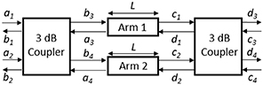
Figure 4. 2 ×2 switch cell block diagram (a1≡ In1 , a2≡ In2 , d3 ≡ Out1 and d4 ≡ Out2 with respect to figure 2).
Download figure:
Standard image High-resolution imageThe 2 × 2 MZI switch can be mathematically described as:

where S2×2 is the global 4 × 4 matrix of the switch cell. SC represents the scattering matrix of the 3 dB coupler, and is given by:

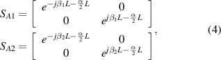
SA is the 4 × 4 matrix related to the two MZI arms and is given by:

where 2 × 2 SA 1 and SA 2 represent the matrices of MZI arm 1 and arm 2, respectively. By taking into account both forward and backward waves, they are given by:
where  (i = 1, 2), with α the propagation loss and neffi the effective refractive index of the ith arm of the MZI in figure 4.
Assuming the input at In1, switching from Out1 to Out2 is obtained by modulating the phase difference Δϕ between the two arms with only one phase shifter (single-ended operation) on arm 1, as in figure 2. In particular, the phase shifter must cause a change in the refractive index Δn, which is able to generate a π-phase shift (Δϕ = π). In this case, the terms of  matrix are accordingly changed by taking into account the change in
  induced by Δϕ. In the cross state, no phase tuning is required, i.e. Δϕ = 0, which means that β1
= β2
= β.
induced by Δϕ. In the cross state, no phase tuning is required, i.e. Δϕ = 0, which means that β1
= β2
= β.
The design of the main building blocks of the proposed device, as the single-mode waveguide, the 3 dB SWG coupler and the TO phase shifter, will be described in sections 3.1–3.3, respectively. Finally, the performance of the proposed structure is reported in section 3.4.
3.1. Single-mode waveguide and bend
The SOI strip waveguide is fully embedded in silicon dioxide, with a width w = 440 nm and thickness h= hmax = 220 nm (figure 3(a)). The overlayer is 1 μm and the substrate 3 μm thick [52].
The size of the waveguide cross-section (440 nm × 220 nm) ensures a quasi-single mode operation, with an neff = 2.325 @ 1550 nm for the fundamental Transverse Electric (TE) mode, the only one that has been considered in the device design flow. The loss value has been derived from the literature and was assumed to be equal to 0.4 dB cm−1 in the range 1500  1600 nm, as achieved for a waveguide of the same material and of the same size, fabricated using high-resolution ArF immersion lithography [52].
To physically split the input and the output of each coupler, adiabatic s-bent waveguides are added at both ends of the coupler. According to [53], a curvature radius of an s-bent waveguide equal to 2 μm has been considered, with a total length of 8 μm. This represents a good compromise between low losses (≈0.2 dB) and footprint compactness (32 μm2).
3.2. 3 dB SWG coupler (SWG-C)
SWGs have been included in the device to ensure broadband operation. In this sub-section, we describe the design of a single directional coupler based on an SWG, aimed at maximizing the wavelength insensitivity and compactness, as demonstrated in [46].
Figure 5 shows the configuration of the SWG coupler. It consists of a conventional directional coupler (DIR-C) with gap g between the two waveguides, an SWG with period Λ and a duty cycle DC. The length Lc ensures a 50:50 splitting ratio, and then, a phase shift of π/2 between the two arms.

Figure 5. Sketch of the SWG-C (w: waveguide width; Lc: coupler length; Λ: period). Bright and shaded grating portions show thickness hmax and hmin, respectively. SWG cross-section is shown in figure 3(b).
Download figure:
Standard image High-resolution imageSeveral degrees of freedom can be identified for the design of this component as the gap g, thickness difference Δh = hmax − hmin, period Λ and duty cycle DC. The coupler length Lc must be kept independent of the operating wavelength. First, since hmax = 220 nm, a gap g ⩾ 200 nm would ensure an aspect-ratio of the grating that does not imply any serious issues to manage during the fabrication steps, thus also safeguarding the replicability of the process. Thus, a gap g = 200 nm has been chosen, which also allows one to maximize the device compactness. The coupling length Lc dependence on the operating wavelength λ has been investigated for several values of Δh, by using the CMT, as in [54].
Sellmeier relationships for the refractive index dispersion in silicon [55] and silicon dioxide [56] have been taken into account.
According to the theory [40], SWGs can be considered lossless if the fabrication process is extremely controlled and reliable. For the 3 dB SWG coupler, as conventionally reported in the literature [46], we have assumed excess losses, usually caused by grating residual reflections, evanescent fields in the coupling regions, as well as surface roughness or any other changes in the SWG physical and/or geometrical parameters with respect to the nominal ones. The excess losses strictly depend on the grating characteristics, the geometry of the coupling regions, as well as the coupler length. The losses induced by the coupler section made of SWGs have been calculated by assuming in our simulations an overestimated value equal to 4 dB cm−1 to account for all the above-mentioned contributions, in case they are really present.
As initial conditions for the design, a period Λ = 300 nm and duty-cycle DC = 50% have been considered, which also takes into account the fabrication tolerances because the value of the aspect ratio Λ/g ⩾ 1 can be controlled with high accuracy using standard manufacturing processes. The period has been set through the Bragg condition, where  , with n1 and n2 the effective index of a slab waveguide with thickness hmax and hmin, respectively [57, 58].
A minimum λB = λmin = 1500 nm has been assumed. The trend achieved for Λ as a function of Δh is shown in figure 6.

Figure 6. Λ fulfils the Bragg condition λB = λmin = 1500 nm as a function of Δh. With a minimum period Λ = 320 nm the operation is in the subwavelength regime for Δh ranging from 0–220 nm.
Download figure:
Standard image High-resolution imageWhen Δh increases,  and, in turn, Λ increase, a minimum period Λ = 320 nm ensures the operation in the subwavelength regime for Δh ranging from 0–220 nm.
In order to take into account the SWG bandgap width, and any manufacturing issues that could affect the device performance, a period Λ of 300 nm has been considered with a conservative approach.
The Lc versus λ trend is reported in figure 7(a) for several values of Δh. The average derivative of Lc with respect to λ, (∂Lc
/∂λ) [m/m] has been calculated in the range λ = [1500 nm ÷ 1600 nm] (see figure 7(b)) to verify the possibility of achieving flat Lc behaviour with wavelength, and, then, the minimum value of ∂Lc
/∂λ vs Δh. The flatness of the Lc versus λ is strictly related to the intrinsic nature of the SWG. At subwavelength scale, the SWG can be approximated by an effective homogeneous structure, with effective refractive index  , dependent on the grating characteristics that also mitigate the dispersion effect. According to the supermodes theory, this results in a lower than the effective refractive index of the straight bare waveguide (Δh = 0) and decreases with the increase in the modulation depth because the evanescent field increases with a higher coupling coefficient between the two coupler arms. Furthermore, the dispersion mitigation leads to a significant decrease in wavelength dependence of Lc on the
  decrease and, then, on the increase in the modulation depth Δh. In fact, as shown in figure 7, the presence of the SWG allows the decrease in the slope, with a significant saving in terms of footprint with respect to a conventional coupler (Δh = 0). As can be seen, Δh = 220 nm is the best value to achieve a broad operating range for the proposed SWG-C.

Figure 7. (a) Coupling length Lc versus wavelength λ for Δh = 0 nm, which corresponds to the conventional coupler, Δh = 80, 140 and 220 nm; (b) trend of ∂Lc /∂λ in the range 1500 nm ÷ 1600 nm for several values of Δh.
Download figure:
Standard image High-resolution imageAfter setting the thickness difference Δh, the dependence of Lc on period Λ has also been investigated, by assuming Δh = 220 nm and DC = 50%. Lc versus λ for different Δh values, and the relative average derivative ∂Lc /∂λ in the range λ = [1500 nm ÷ 1600 nm] for several values of Λ are shown in figures 8(a) and (b), respectively. We have assumed a minimum period Λ = 200 nm to guarantee the feasibility of the current manufacturing process. As shown in figure 8(b), Λ = 260 nm shows the minimum derivative value (≈1.5 [m/m]).

Figure 8. (a) Coupling length Lc versus wavelength λ for Λ =100 , 200, 280 and 300 nm; (b) trend of the average value of ∂Lc /∂λ in the range 1500 nm ÷ 1600 nm for several values of Λ.
Download figure:
Standard image High-resolution imageFor Λ > 260 nm, the resonances at the photonic band-edge affect the SWG coupler operation, resulting in an increase in the ∂Lc /∂λ slope, while for Λ < 260 nm, the light propagating within the SWG is no longer affected by the presence of the grating itself. Furthermore, Λ = 260 nm would facilitate the manufacturing of the SWG coupler because the ratio between the etch depth and minimum pitch is about 50%.
Finally, the duty cycle has also been determined to improve the operating bandwidth of the proposed device. The coupling length Lc in the wavelength range 1500 nm ÷ 1600 nm for DC = 25%, 50% and 75% is reported in figure 9(a). Figure 9(b) depicts the trend of ∂Lc /∂λ versus DC.

Figure 9. (a) Coupling length Lc versus wavelength λ for DC = 25%, 50% and 75%; (b) trend of the average value of ∂Lc /∂λ in the range 1500 nm ÷ 1600 nm for several values of DC.
Download figure:
Standard image High-resolution imageAgain, minimum and maximum values of DC equal to 25% and 75%, respectively, have been taken into account to guarantee the SWG fabrication feasibility. For large values of DC, the SWG tends to behave as an unperturbed waveguide, with an increase in  , and then the slope ∂Lc
/∂λ of the curve increases, while, for small values of DC, the sub-wavelength regime is enhanced with a decrease in
, and then the slope ∂Lc
/∂λ of the curve increases, while, for small values of DC, the sub-wavelength regime is enhanced with a decrease in  and, then, of ∂Lc
/∂λ, at the expense of a more difficult fabrication process. Thus, the condition DC = 50% represents the best compromise to obtain a broad operative wavelength range, together with easy fabrication.
and, then, of ∂Lc
/∂λ, at the expense of a more difficult fabrication process. Thus, the condition DC = 50% represents the best compromise to obtain a broad operative wavelength range, together with easy fabrication.
Moreover, the transmission spectrum of the device with g = 200 nm, Λ = 260 nm, DC = 50% and Δh = 220 nm has been simulated by using a 2D FDTD technique. We consider the light as launched from the left into the upper waveguide (In1,c ≡ a1) (see figure 2). P1 and P2 denote the powers at the output ports Out1,c and Out2,c , respectively.
At the same output ports, the normalized powers can be defined as η1 and η2 , respectively:

Figure 10 shows the η1 (%) and η2 (%) spectra for the optimized SWG-C, assuming several semi-periods NP of the grating equal to 19, which leads to Lc = 2.47 µm that fits with the estimated value reported in figure 9(a). An odd number of semi-periods allows one to consider the coupler as symmetrical.

Figure 10. Coupling ratios η1 and η2 versus wavelength for a power-splitting ratio of 50/50.
Download figure:
Standard image High-resolution imageThe wavelength insensitivity of the Lc leads to a bandwidth coverage of 100 nm by the SWG coupler, with a maximum imbalance of ±9% in the range 1500–1600 nm or bandwidth of 150 nm, with a maximum imbalance of ±13%, extending the range to 1650 nm. The overall footprint of the device results is very compact (≈19 µm × 9 µm). The coupling ratios of our device have been compared with those of a DIR-C, with a gap of 200 nm and Lc = 7 µm. The results (figure 11) show that the conventional coupler has a ±15% power imbalance over 100 nm bandwidth (figure 11(a)) and this imbalance increases with increasing bandwidth (see figure 11(b)).

Figure 11. Cross- coupling ratio of the output power of the designed SWG coupler (SWG-C) compared to a conventional directional coupler (DIR-C) over (a) 100 nm bandwidth and (b) 300 nm bandwidth.
Download figure:
Standard image High-resolution imageThe average insertion loss of the proposed 3 dB SWG-based directional coupler over a bandwidth of 150 nm is −3.8 dB, including the loss of the S-bend and coupling region. An excess loss of 0.8 dB was calculated.
3.3. TO phase shifter
Figure 12 shows the cross-section of the phase shifter. It consists of a TiN layer 100 nm thick and wH wide placed on top of the silicon core waveguide at a distance d.

Figure 12. Temperature distribution in the cross-section of the phase shifter.
Download figure:
Standard image High-resolution imageThe phase shifter operation is based on the TO effect. In a broadband silicon TO switch, the switching is obtained by thermally shifting the optical phase by π in one of the waveguide arms of an MZI. In most applications, achieving a high switching speed with minimal power is desired. However, these two goals are at odds.
In order to optimize the TO tuner design, a figure of merit (FOM) is used, defined as:

where ΔTπ and H are the temperature to achieve a π shift and the heat capacity of the heater arm, respectively, Pπ and τ are the power required to achieve a π-phase shift in one arm of the interferometer and the thermal time constant, respectively. The latter is expressed as:
where G is the thermal conductance between the heated waveguide and the heat sink (i.e. the substrate), and A is the area traversed by the heat flow (i.e. the waveguide cross-section perpendicular to the heat flux).
For a π-phase shift [59] we have:

where nSi is the refractive index of the silicon and L the length of the phase shifter.
Increasing L effectively lowers ΔTπ , which reduces lateral crosstalk. However, the device footprint, propagation loss and the voltage needed to achieve a π shift all increase proportionally to L (assuming the heater resistance Req,h∝ L). Therefore, in practice, L is made small enough. It is important to note that L affects neither Pπ nor τ since both A and H are ∝ L.
Furthermore, since ∂n/∂T is a fixed material property, the only way to truly improve the heater FOM is to reduce the heat capacity H or, in other words, decrease the thermal energy required to increase the waveguide temperature [59]. This is typically achieved by bringing the heat source as close as possible to the waveguide while limiting optical loss, especially if a low thermal conductivity material (oxide) separates the heater and waveguide. By feeding the metal layer with power Pπ, the effective index change, with an associated optical loss α, is negligible (α ≈ 3.814 × 10⁻³ dB cm−1) because the heater is high enough above the waveguide. Metal heaters cannot be made arbitrarily thick because of fabrication constraints that limit metal layers here to thicknesses in the order of 100 nm [60].
The TO phase shifter has been designed using the FEM approach. Simulations were done by combining a thermal solver and an optical mode solver, to analyze the heat distribution, efficiency and transient response. The metal chosen for the heater is titanium nitride (TiN), due to its good chemical and thermal stability, high hardness and corrosion resistance [61, 62]. It is placed on the Si strip waveguide at a distance d. The heater total length L has been set to 200 µm without any impact, neither on Pπ nor on τ.
The simulations have been carried out by considering the TiN electrode fed by power Pπ , the complex thermal conductivity of all layers of the device cross-section and a temperature of 300 K as a boundary condition of the simulation domain. To optimize the design to achieve low power consumption and maximize (with the minimum value of power time product) the FOM, calculations assuming different values of distance d and microheater width wH have been carried out.
The effect of the heater width on Pπ and τ for different values of d has been investigated. The results from both the steady state and the transient analyses have shown that reducing the heater width has little effect on the switching time but results in a power saving. The latter can be attributed to the reduction in heat loss when the transverse heat conduction path from the heater to the waveguide core occurs as the cladding thickness is reduced.
Power consumption can also be reduced by increasing the thickness of the upper cladding through the increase in the heat insulation instead of the heat conduction.
Figure 13 shows the heater FOM; it can be seen that as heater width wH and oxide thickness d decrease, the FOM also decreases. This can be justified by the fact that the switching power and time are reduced when the heater is brought closer to the waveguide. In order to minimize the FOM, wH = 0.8 µm and d = 0.4 µm have been fixed for the TiN microheater, whose cross-sectional view is shown in figure 12.

Figure 13. FOM versus wH for various values of oxide thickness d.
Download figure:
Standard image High-resolution imageΔn and ΔT have been calculated for several values of the power applied to the heater. A temperature shift ΔT = ΔTπ ≈ +20 K in the waveguide core is necessary to induce a π-shift over a 200 µm length of the above-sized microheater.
It can be seen that as the power applied to the heater increases, the heater temperature increases too, causing a consequent increase in the effective index difference of the phase shifter.
Figure 14 shows a step transient response for d= 0.4 µm and wH= 0.8 µm. We have estimated Pπ = 11.5 mW and tr = 9.2 µs, calculated as the time between 90% and 10% of the time response. The calculated Pπ and tr are in good agreement with experimental data reported in the literature [59, 60].

Figure 14. Transient analysis: temperature versus time at the waveguide core when the heater power is turned on (0 → Pπ ).
Download figure:
Standard image High-resolution image3.4. 2 × 2 MZI switch performance
Based on the results obtained from the design of the individual switch components and simulation of the entire device, we have derived the transmission spectrum of the designed 2 × 2 MZI switch in the cross and bar state, as illustrated in figures 15(a) and (b). The bar state behaviour, shown in figure 15(b), is similar to the standard MZI one [31], with a significant increase in the bandwidth, which results in acceptable crosstalk values, while the power imbalance of the SWG-based coupler, as shown in figure 11, leads to several ripples, with the worst-case amplitude of 15 dB, in the cross-state spectra (see figure 15(a)).

Figure 15. Normalized transmission spectra Pout of the designed 2 × 2 MZI switch, as in figure 2, by considering In1 as the input: (a) cross state, (b) bar state.
Download figure:
Standard image High-resolution imageIn both switching states, the device can operate over a bandwidth of 153 nm, delimited by the dotted black vertical lines, ranging from 1500–1653 nm, with a worst-case ERsw of about 13 dB for the cross state (λ ≈ 1.62 µm) and 19 dB for the bar state (λ ≈ 1.65 µm). The calculated worst-case crosstalk (XTsw) is about −12 dB over the whole bandwidth of 153 nm with a worst-case insertion loss (ILsw) of less than 2 dB, both related to the cross state. The device footprint is about 240 µm × 9 µm.
Compared to other switch configurations reported in the literature [31–34], the proposed device shows a very large operating bandwidth within a very small footprint, with power consumption and switching time according to the literature [59, 60].
4. 8 × 8 dilated Banyan matrix design
An elementary cell was used as a building block of an 8 × 8 matrix based on dilated Banyan topology [63, 64], as in figure 16. This topology allows the suppression of first-order crosstalk since only one signal at a time passes through a cell. To ensure strictly non-blocking behaviour, each switching element routes just one system call, avoiding any interference between two different signals. Therefore, there is always a free path for a new system call. The 8 × 8 matrix consists of six stages, respectively, with 8, 16, 32, 32, 16 and 8 sorters. The coloured lines in figure 16 represent the optical paths, with the minimum propagation lengths needed to obtain the signal routing from the input ij to the output oj (i = 1,..., 8) ports, with non-blocking behaviour. As reported in [64], the connections i1 − o3 , i2 − o7 , i3 − o5 , i4 − o1 , i5 − o6 , i6 − o2 , i7 − o4 and i8 − o8 enable the routing of eight channels with non-blocking behaviour, also suppressing the crosstalk. In particular, according to [65], the crosstalk XTm of a dilated Banyan switching matrix can be expressed as: XTm = −2XTsw−20log10(2log2 N −1) + 3, where XTsw is the crosstalk of 2 × 2 MZI and N is the number of input/output ports. Since XTsw is equal to −16.82 and −11.56 dB for the bar and cross state, respectively, and N = 8, an average crosstalk XTm equal to about −38 dB has been calculated by using the above equation.

Figure 16. Schematic of an example 8 × 8 dilated Banyan switch matrix with established connections i1 − o3, i2 − o7, i3 − o5, i4 − o1, i5 − o6, i6 − o2, i7 − o4, and i8 − o8. Grey boxes correspond to the device sketched in figure 5.
Download figure:
Standard image High-resolution imageWaveguide crossing has been properly designed to have a smaller insertion loss with respect to the 90° simple crossing components [66]. The design is based on the configuration proposed in [67] and shown in figure 17(a). Particle swarm optimization [68], combined with the FDTD method, has been used to optimize the design.

Figure 17. (a) Schematic of the waveguide crossing. Device is symmetric and constituted by four identical tapers. Geometrical variation of the taper width wcross(x) along the taper length Lcross, is reported in (b).
Download figure:
Standard image High-resolution imageThe optimization process is based on maximizing a new FOMT defined as the average transmission (over wavelength) at the crossing through port (T3) minus the transmission at the crossing ports (T2 + T4) and the reflection (R1) at port 1: FOMT = T3 − T2 − T4 − R1.
The crossing consists of four identical arms, and each arm is drawn using spline interpolation. Four short straight strip waveguides are appended to the tapers to lead-in/lead-out light. A sketch of the designed taper widths wcross (x) along the taper length Lcross (=4.6 µm) is reported in figure 17(b). The simulated transmission contour plot and the transmission spectra, by considering Port 1 ≡ 1, are shown in figure 18.

Figure 18. (a) Transmission contour plot of the designed waveguide crossing at 1550 nm. (b) Transmission spectra over 100 nm bandwidth of Port 2, Port 3, and Port 4, by considering Port 1 as the input port. At Port 1, a backscattering power of about −40 dB has been calculated.
Download figure:
Standard image High-resolution imageThe design of the waveguide crossing has been optimized for a wavelength of about 1550 nm. Working over a bandwidth of 153 nm, a worst-case IL of 0.077 dB and XT of −36.95 dB has been obtained.
The spectrum relevant to the eight paths analyzed, as in figure 16, has been calculated.
Figure 19 shows the simulated transmissions of the 8 × 8 switch matrix, for the established connections reported in figure 16. Transmission values within the operating bandwidth of 153 nm, that lead to the worst-value XTm, have been considered.

Figure 19. Output transmissions of the 8 × 8 switch with idle switches randomly in the cross or bar states.
Download figure:
Standard image High-resolution image
The results show the worst output crosstalk XTm ≈ −38 dB (for the connection i7 − o4), which is compliant with the calculated one, ERm ≈ 53 dB and ILm ≈ 15 dB, again in the worst case, with a significant saving in terms of power consumption (276 mW). A footprint approximately equal to 1620 µm × 576 µm has also been estimated for the whole Banyan switching matrix. Table 1 summarizes the worst-case performance of the designed switch matrix.
Table 1. Worst-case performance of the 8 × 8 dilated Banyan switch matrix.
| Parameter | Unit | Value |
|---|---|---|
| Number of In/Out | 8 | |
| Insertion Loss (ILm) | dB | 15 |
| Extinction Ratio (ERm) | dB | 53 |
| Crosstalk (XTm) | dB | −38 |
| Switching time | µs | 9.2 |
| Power consumption | mW | 276 |
The results obtained for the Banyan matrix are very encouraging for the use of our switching cell in TLC payloads and for all applications that require a large bandwidth. In fact, as for the operating bandwidth, the proposed device is suitable for complex multi-channel multiplexing services. In particular, for an optical transmission network in a telecom satellite based on dense wavelength division multiplexing that requires a channel spacing of more than 100 GHz, wavelength-insensitive performance over a bandwidth of more than 150 nm, which enables multi-service routing of up to 95 and 190 channels, for a spacing of 200 and 100 GHz, respectively.
The insertion loss of the matrix is strictly dependent on the losses of the switching cell, whose value we have obtained, but it needs to be further reduced. A significant decrease in insertion losses can certainly be seen both considering the continuous improvement in the manufacturing technology and the number of matrix inputs/outputs (e.g. for a 4 × 4 switching matrix using the proposed cell, the insertion loss is around 8 dB or less).
Recently, besides the use of switching devices in TLC payloads, further Space applications of photonic switches are emerging, including optopyrotechnics, atom sensors and laser interferometry, although with different specifications. Optopyrotechnics requires a number of ports > 2, XT < −50 dB and IL < 1; atomic sensors, number of ports > 4, IL < 1 and the XT is a non-limiting factor; laser interferometry, number of ports > 2, IL < 1 dB and the XT is a non-limiting factor [20]. Since the proposed device fulfils some critical performance among the requested ones, additional investigation aimed at improving the overall characteristics of the proposed device is needed in order to make it suitable for a wider range of applications.
5. Conclusions
In this paper, we have proposed the design of a broadband switching device as a key element of switching matrices for telecommunication satellite payloads that require the routing of a signal with large bandwidth. The switching device is a 2 × 2 Mach–Zehnder interferometric switching cell, whose critical component is a 3 dB coupler based on an SWG.
The proposed coupler exhibits better performance in terms of balanced coupling compared to conventional couplers of the same size. It is also competitive in terms of size, and operation bandwidth (≈150 nm) and can be easily integrated with CMOS electronics. Furthermore, for the MZI operation, a low-power phase shifter based on a TiN heater has been theoretically demonstrated.
As an example, the performance of an 8 × 8 dilated Banyan switch matrix made by the new 2 × 2 switch as a building block has been estimated, and was found to agree with the specifications required for TLC payloads in terms of ER, crosstalk, power consumption and switching time over a broad bandwidth.
A variety of emerging applications in Space can be envisaged for this kind of photonic switch, as mentioned above.
Acknowledgments
The work has been supported by the Ministry of Research and University in the framework of New Satellites Generation components (NSG) Project (No. ARS_01_01_2015).
Data availability statement
All data that support the findings of this study are included within the article (and any supplementary files).