

Abstract
We investigated highly mismatched InAsSb photodiodes (PDs) grown on GaAs substrates working in the long-wavelength-infrared range (8–12 μm). Because of their low absorption coefficient levels and high Auger recombination rates, InAsSb PDs suffer from several difficulties, including low responsivity and low resistance levels at room temperature. Additionally, the large lattice mismatch between the active layer and substrate material introduces a high density of dislocations and thus degrades performance. In the work described in this report, we realized high-performance InAs0.13Sb0.87 PDs by reducing the density of dislocations as a result of applying a dislocation filter structure, as well as by optimizing interference within the active layer. The resulting device (cut-off wavelength of about 11 μm) showed, at room temperature, a resistance R0 of 90 kΩ and responsivity Ri of 0.47 mA W−1 at a wavelength of 9.5 μm, leading to a high detectivity D* of 1.2 × 108 cm Hz1/2 W−1, which is suitable for detecting alcohol.
Export citation and abstract BibTeX RIS
1. Introduction
Opto-electronic devices working in the mid-infrared wavelength range (2–10 μm) have several important applications, including thermal imaging and environmental gas monitoring. Above all, the emerging gas sensing market has been attracting increasing attention owing to the recent concerns about indoor air quality and greenhouse gas emissions [1, 2]. Recent technological progress in mid-infrared light-emitting diodes (LEDs) and photodiodes (PDs) have made it possible to realize high-resolution low-power-consumption gas-sensing modules deploying non-dispersive infrared (NDIR) absorption technology [2]. However, only optical devices (LEDs and PDs) operating at relatively short wavelengths, such as 4.3 μm for CO2 and 3.3 μm for CH4 have been put to practical use. This limited use is due to difficulties in applying such devices in the long-wavelength regime, with such difficulties including degradation of device performance as a result of extra Auger recombination loss [3]. On the other hand, the need for optical devices operating at long wavelengths is increasing. For example, alcohol-sensing and freon-sensing are emerging areas of interest. Especially, the former application is attracting attention in efforts to reduce accidents caused by driving under the influence of alcohol [4]. Alcohol (i.e. ethanol) absorbs light at a wavelength of about 9.5 μm [5, 6]. For this wavelength vicinity, thermal detectors such as thermopile and pyro-electric detectors has been widely recognized as the best choice [7]. However, the slow responses of such thermal detectors have led to drawbacks such as relatively high power-consumption and undesirable noise characteristics (flicker noise) due to inabilities to achieve high-frequency chopping and intermittent operation.
There have been several reports on PDs operating in the long-wavelength regime. Compound semiconductor materials such as HgCdTe [8, 9] and InAsSb [10–14] ternary alloys have been investigated as active layer materials for PD detectors. These materials show excellent performances at low temperatures (e.g. 77 K). However, they suffer from significant performance degradation with increasing temperature, because of their narrow bandgaps. Therefore, it is important to realize high-performance mid-infrared PDs that work at room temperature. The Detectivity D* of a PD is proportional to the responsivity Ri and the square root of the resistance-area product (RA) [3], and hence to realize a high-detectivity PD, it is important to increase both the responsivity and RA of the device. Additionally, achieving a high output resistance R0 of a PD is also important for practical applications in order to reduce noise from the rear stage amplifier circuit [15].
In the work described in this paper, we fabricated high-detectivity and high-resistance InAsSb PDs with a cut-off wavelength as high as 11 μm. A high detectivity of 1.2 × 108 cm Hz1/2 W−1 at a wavelength of 9.5 μm was achieved even at room temperature, and hence a device comparable to thermopile was produced.
These findings could contribute to the realization of a high-resolution and low-power-consumption NDIR alcohol sensing modules.
2. Experimental
Schematic cross sections of the InAsSb PDs used in this work are shown in figures 1(a) and (b). Figure 1(a) shows a conventional PD structure, and figure 1(b) shows an improved device structure with dislocation filter layers, as discussed below. The structure was grown by molecular beam epitaxy (MBE: MBE 49, RIBER) on a semi-insulating GaAs (100) substrate.

Figure 1. Schematic of the film structure for the InAsSb photodiode (a) without and (b) with dislocation filter layers.
Download figure:
Standard image High-resolution imageThe dislocation-filter-layer-containing InAsSb PD structure (figure 1(b)) was prepared as follows. First, a 0.5 μm thick Sn-doped n+-InSb buffer layer was grown at 410 °C on a thermally cleaned GaAs substrate, followed by a 1.1 μm thick Sn-doped n+-Al0.09In0.91Sb buffer layer. Two dislocation filter layers, which are 20 nm thick Sn-doped (n+) Al0.32In0.68Sb layers, were inserted within the buffer layer to reduce the density of dislocations by confining them within strained layer interfaces [16, 17]. Then, a 2.4 μm thick Zn-doped InAs0.13Sb0.87 active layer was grown, which was sandwiched between 20 nm thick Sn-doped (n+) Al0.18In0.82Sb and Zn-doped (p+) Al0.18In0.82Sb as hole- and electron-blocking barrier layers, respectively. Finally, on top of this stack was grown a 0.5 μm thick Zn-doped p+-InSb top layer to form a complete PD film structure. The n-type and p-type layers were doped with Sn at a concentration of 7.0 × 1018 cm−3 and with Zn at 2.0 × 1018 cm−3, respectively. The Zn concentration in the active layer was controlled to be 5.4 × 1017 cm−3 to suppress both Auger recombination and band-filling caused by thermally excited degenerate electrons [14, 18, 19].
The thin film structure was processed into mesa-type PD sensors using a conventional semiconductor fabrication technique described elsewhere [20]. SiO2 was used as surface passivation layer to protect the InAsSb side wall, after which SiNx was deposited.
Figure 2 shows a photograph of an InAsSb PD chip and a schematic cross-section of a single p-i-n junction of this PD. A total of 1,567 p-i-n mesa PDs with a junction area of 230 μm2 were connected in series within a 1.1 mm square chip to increase the output resistance R0, and hence help reduce electrical noise caused by rear-stage amplifier circuits [21]. We adopted the backside illumination architecture, i.e. the incident mid-infrared light was illuminated from the substrate side to eliminate shadow loss. The frontside of the device was mostly covered with metal layers (Au/Pt/Ti) to reflect transmitted light back to the active layer. Dislocations in the film were analyzed in cross-sectional and plane-view scanning transmission electron microscopy (STEM; HD-2300, Hitachi) images [16]. Bright-field images were taken in the (1 −1 0) and (0 0 1) directions for the cross-sectional and plane-view dislocation analyses, respectively.

Figure 2. (a) Photograph of a 1.1 mm × 1.1 mm InAsSb photodiode chip and (b) a schematic of a cross-section of a single p-i-n junction of the InAsSb photodiode.
Download figure:
Standard image High-resolution imageRA was evaluated by multiplying the resistance for a single p-i-n junction and its area at room temperature (25 °C). Specific detectivity D* was calculated from normal incidence spectral responsivity Ri and zero-bias diode resistance. Spectral responsivity was measured using a Fourier-transform infrared spectrometer (Nicolet8700, Thermo Fisher Scientific), and the absolute value was obtained using a 500 °C blackbody radiation source, calibrated with a thermopile detector. The electrical and optical properties were characterized at room temperature (25 °C) unless otherwise stated.
3. Results and discussion
Figure 3 shows (a) responsivity (Ri ) and (b) external quantum efficiency (EQE) spectra for conventional InAsSb PDs (figure 1(a)). As compositions for the active layer was varied to 0, 0.06, 0.094, 0.133, and 0.188. Other parameters are listed in table 1. A reduction of Ri , and red shift of the cut-off wavelength were clearly observed with increasing As composition. Also two unusual behaviors were observed here. First, Ri and EQE even at short wavelengths (3–5 μm) showed systematic reductions with increasing As composition, i.e. with decreasing bandgap energy [22]. Generally, a reduction in bandgap results in an increased absorption coefficient at the same wavelength. Therefore, these reductions in Ri and EQE indicated a reduction in carrier extraction efficiency. Secondly, unevenness in each of the Ri and EQE spectra was observed at long wavelengths (from 7 to 11 μm). In this material system, the absorption coefficient of the InAsSb active layer at a wavelength of 9.5 μm is quite low [14]. Additionally, due to this wavelength within the active layer being comparable to the thickness of the active layer, interference of incident infrared light within the film structure was expected to be non-negligible, a point addressed below.
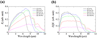
Figure 3. (a) Ri and (b) EQE spectra for various InAsSb photodiodes with different As compositions, namely 0.00, 0.060, 0.094, 0.133, and 0.188.
Download figure:
Standard image High-resolution imageTable 1. Film structure parameters for InAsSb photodiodes, including active and barrier layer.
| InAsSb active | AlInSb barrier | |
|---|---|---|
| As composition | Zn concentration (cm−3) | Al composition |
| 0 | 6.0 × 10¹⁶ | 0.18 |
| 0.060 | 4.0 × 10¹⁷ | 0.23 |
| 0.094 | 4.0 × 10¹⁷ | 0.23 |
| 0.133 | 5.4 × 10¹⁷ | 0.23 |
| 0.188 | 9.4 × 10¹⁷ | 0.23 |
Figure 4 shows current density–voltage (J–V) curves for various InAsSb PDs with different As composition, namely 0.06, 0.094, 0.133, and 0.188. The current density systematically increased with increasing As composition, indicating increase in recombination rate within the active layer, which means shorter carrier life time. This trend is consistent with the reduction in EQE for high As composition, where shorter carrier life time leads to lower carrier extraction efficiency (lower EQE).
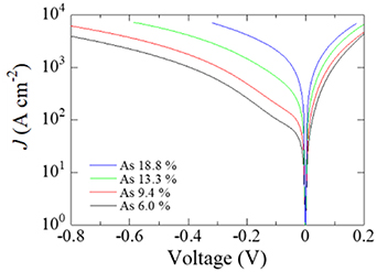
Figure 4. J–V curves for various InAsSb photodiodes with different As compositions, namely 0.060, 0.094, 0.133, and 0.188.
Download figure:
Standard image High-resolution imageIn order to investigate the recombination process, electroluminescence behavior was also investigated. Figure 5(a) shows emission spectrum and figure 5(b) the optical power and EQE as a function of injection current density for an InAs0.133Sb0.867 LED, which has the same film structure as shown in figure 1(a). This LED yielded broad emission spectrum with a peak and cutoff wavelength at 8 μm and 11 μm, respectively. A monotonic decrease in EQE with increasing injection current density was observed (figure 5(b)). This result indicate that Auger recombination has appreciable fraction in total recombination processes even at low injection current regime. Therefore, decrease in carrier life time, deduced from the Ri and J–V results shown in figures 3 and 4, is partly due to the increased Auger recombination process.
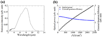
Figure 5. (a) Emission spectrum and (b) optical power-input current density (J) characteristics for InAs0.133Sb0.867 photodiodes. External quantum efficiency is also shown on the right axis (b).
Download figure:
Standard image High-resolution imageA bend in the EQE at low injection current indicates existence of defect induced recombination [23, 24]. Although, it is difficult to suppress Auger recombination, there is room for improvement and optimization in device performance from the perspective of optical interference and dislocation reduction.
In order to optimize the effect of interference within the film structure at 9.5 μm, we performed an optical simulation using COMSOL Multiphysics® software. As mentioned above, interference was considered to be non-negligible due to the low absorption coefficient in the device structure (figure 1). In general in such set ups, light incident to the film stack transmits from the substrate side to the top metal contact, and reflects back to the direction of the incident light, resulting in interference of light within the film. In order to achieve high responsivity, it is important to increase the absorption within the active layer or, in other words, minimize the reflectance of incident light from the film stack. This goal could be achieved by adjusting the thickness of the active layer. This phenomenon is similar to the case of anti-reflection coating or impedance matching in high-frequency electronics circuits (transmission line), whose reflectance could be controlled by the length of the stub.
Finite element analysis of Helmholtz equation was performed on a model of a single p-i-n junction under periodic boundary condition. Incident light has wavelength of 9.5 μm and has incident angle normal to the film. The results of our simulation showed a clear interference pattern of the electric field intensity distribution for InAsSb PDs (figure 6(a)). Figure 6(b) shows the reflectance as a function of the active layer thickness. Reflectance was indicated to oscillate with increasing active layer thickness, showing minimal value at integer multiples of about 1.2 μm., a value corresponding to a half wavelength of 9.5 μm within the active layer (with the refractive index for the InAsSb active layer being about 4.0 at 9.5 μm). Figure 6(c) shows the absorptance of incident light at each layer as a function of the active layer thickness. An oscillation of absorptance in the active layer was also observed, and corresponded to that of the reflectance. As previously mentioned, the cause of these oscillations are the interference within the film stack. It is known that InAsSb has quite low absorption coefficient (∼1300 cm−1) [14]. Because of the difference of the film material or refractive index within the film stack together with the low absorption coefficient, positive and negative interference occurs with varying active layer thickness.
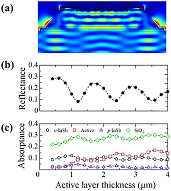
Figure 6. (a) Simulated electric field intensity distribution within an InAsSb photodiode p-i-n junction. (b) Reflectance and (c) absorptance of incident light each as a function of the thickness of the active layer for InAsSb photodiode.
Download figure:
Standard image High-resolution imageAs the thickness of the active layer was increased, higher absorptances were observed, leading to higher responsivity levels due to the increased optical density. However, a thicker active layer would also lead to lower resistance because of increased rate of carrier recombination within the active layer, which would cause a reduction in the detectivity [17]. Therefore, in order to achieve the best tradeoff here, the active layer thickness was set to 2.4 μm in this study, where reflectance and absorptance show local minimum and maximum respectively.
Additionally, high absorptance was observed at the SiO2 layer as shown in figure 6(c). Though SiO2 works well as a surface passivation layer for InAsSb, absorption loss becomes specifically considerable at about 9.5 μm due to the stretching vibration mode of the Si-O bond [25]. Therefore, a quite thin layer of SiO2 was used (20 nm).
Dislocations have previously been shown to detrimentally affect electrical properties in narrow-bandgap materials such as AlInSb ternary alloys [16, 17]. The occurrence of the above-described bend in the EQE curve at low injection current density (figure 5(b)) indicated that dislocations also affected device performances of the InAsSb PDs.
The density of dislocations within an active layer can be reduced by inserting a strained thin layer, namely a dislocation filter layer [16, 17, 26], whose film structure is shown in figure 1(b). Figure 7 shows an X-ray diffraction (XRD) reciprocal space map in the vicinity of the (−1 −1 5) diffraction peak for the InAsSb PD with dislocation filter layers. Because each layer in the film stack has different lattice constants, diffraction peak shifts according to their state of strain-relaxation. The peak assignment of each layer is shown in the figure. Considering the growth procedure, each layer is in a state as follows. First layer of the film stack, i.e. n-InSb layer, is relaxed on GaAs substrate, which is followed by relaxed n-AlInSb (1st). Second and third n-AlInSb layers, dislocation filter layers and barrier layers are strained, and lattice matched with relaxed InAsSb active layer (in-plane lattice constant).
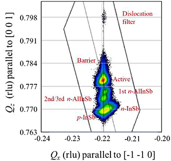
Figure 7. XRD reciprocal space map in the vicinity of the (−1 −1 5) diffraction peak for the InAsSb photodiode with dislocation filter layers. Peak assignment of each layer is shown.
Download figure:
Standard image High-resolution imageFigure 8 shows (a) a cross-sectional and (b)–(e) plan-view STEM images for an InAsSb PD structure in figure 1(b). As with the case with an AlInSb PD, dislocations were stopped at the dislocation filter layers and AlInSb/InSb interface, where dark contrast indicating confined dislocations were clearly observed [16, 17]. Threading dislocation density was calculated to be (2.0 ± 0.4) × 108 cm−2 from plane view STEM images, which is reduced by factor 1.7 compared to the structure without dislocation filter layers.

Figure 8. (a) A cross-sectional image and (b)–(e) plan-view STEM images for an InAsSb photodiode. Plan-view image (b)–(e) corresponds to specimens at the position indicated by arrows in (a).
Download figure:
Standard image High-resolution imageFigure 9 shows temperature dependencies of RA for InAsSb PDs with and without dislocation filter layers in figure 1, except that they both have active layer thickness of 2.4 μm. Zero-bias RA for the InAsSb PD was increased from 1.06 × 10⁻⁴ Ω cm2 to 1.32 × 10⁻⁴ Ω cm2 by introducing dislocation filter layers at room temperature. The increase in RA can be attributed to the reduction of dislocation-induced Shockley-Read-Hall (SRH) recombination. This is supported by the following observation on the temperature dependence of the RA enhancement ratio. The lower the temperature, the higher the resistance due to the reduced rate of recombination processes which is caused by the reduction of intrinsic carrier. The enhancement in RA, upon including dislocation filter layers, increased with decreasing temperature, from a factor of 1.25 at room temperature to 1.4 at −40 °C, where dislocation-induced SRH recombination becomes dominant compared to radiative and Auger recombination, as shown in figure 9 (right axis).

Figure 9. Temperature dependencies of RA for InAsSb photodiodes with and without dislocation filter layers. Temperature dependence of the RA enhancement ratio upon including the dislocation filter layers is also shown on the right axis.
Download figure:
Standard image High-resolution imageFigure 10(a) shows spectral responsivity Ri and specific detectivity D* spectra for InAs0.13Sb0.87 PDs with the dislocation filter layers as shown in figure 1(b). Specific detectivity D* was calculated by the following equation (1), where Ri is responsivity and T is absolute temperature3
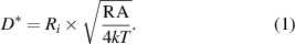
A total of 1567 p-i-n mesa PDs were connected in series with a junction area of 230 μm2. The cut-off wavelength was about 11 μm at room temperature, which corresponds to the bandgap of 0.11 eV. Resistance and responsivity of the device were 90 kΩ and 0.47 mA W−1 at 9.5 μm, resulting in the detectivity of 1.2 × 108 cm Hz1/2 W−1 at 9.5 μm and 2.6 × 108 cm Hz1/2 W−1 at 7.6 μm (peak). This detectivity value was comparable to the performances of thermopiles (widely used thermal detector) and higher than that of the commercially available PD working at the long wavelength mid-infrared range at room temperature [27, 28]. Figure 10(b) shows the temperature dependence of the specific detectivity D* at 9.5 μm for the InAs0.13Sb0.87 PDs. As temperature decreases, the detectivity increases, owing to increased resistance of the PDs. The onset of the decrease in the D* versus temperature curve at low temperatures was caused by a blue shift of the cutoff wavelength.

Figure 10. (a) Responsivity (left axis) and specific detectivity (right axis) spectra for the InAs0.13Sb0.87 photodiode with dislocation filter layers at room temperature. (b)Temperature dependence of specific detectivity at 9.5 μm.
Download figure:
Standard image High-resolution image
4. Conclusions
We investigated highly mismatched InAsSb PDs grown on GaAs substrates working in the long-wavelength infrared range (8–12 μm). High-performance InAs0.13Sb0.87 PDs were realized by optimizing the optical interference within the active layer and reducing the density of threading dislocations by applying dislocation filter layers, which are key difficulties in narrow bandgap materials except Auger recombination loss. The resulting device (cut-off wavelength of around 11 μm) showed resistance R0 = 90 kΩ and responsivity Ri = 0.47 mA W−1 at 9.5 μm leading to a high detectivity of D* = 1.2 × 108 cm Hz1/2 W−1 at room temperature, a value comparable to those of thermopiles and higher than that of the commercially available PD. These results could contribute to the realization of high-resolution and low-power-consumption gas sensing modules, such as for alcohol and freons, in the emerging gas sensing market.
Acknowledgments
The authors thank J Akamine, T Nakao, and T Yamauchi for assistance with the STEM analysis.
Data availability statement
The data generated and/or analyzed during the current study are not publicly available for legal/ethical reasons but are available from the corresponding author on reasonable request.