

Abstract
Complementary metal-oxide-semiconductor inverters featuring steep voltage-transfer characteristics (VTC) were successfully fabricated on 4H-SiC(0001) substrates. Even without nitridation of the MOS interfaces, well-balanced n- and p-channel field-effect transistors were realized by means of ultrahigh-temperature gate oxidation (HTO) at 1600 °C under reduced oxygen partial pressure. Improvements in the performances of both n- and p-channel SiC metal-oxide-semiconductor field-effect transistors were achieved by subsequently performing forming gas annealing (FGA) at 1200 °C, leading to mostly symmetric VTC with negligible hysteresis. The effect of HTO and subsequent FGA at high temperatures was verified from the stable and improved performance of 23-stage ring oscillators over a wide temperature range.
Export citation and abstract BibTeX RIS
Silicon carbide (SiC) is the material of choice for next-generation power-electronic devices with high efficiency and high power density. 1) Following the successful commercialization of SiC-based Schottky barrier diodes (SBDs), full SiC power modules composed of SBDs and metal-oxide-semiconductor field-effect transistors (MOSFETs) are about to expand their field of application. In addition, since the early stages of SiC research, SiC-based complementary MOS (CMOS) integrated circuits have gained attention as emerging electronic devices that can operate in harsh environments. 2–8) Several digital and analog CMOS circuits, such as inverters, ring oscillators, and operational amplifiers, have been integrated on 6H- and 4H-SiC substrates. The reported SiC-based CMOS circuits have exhibited excellent capability of working at temperatures up to 540 °C 6) and superior gamma-irradiation resistance of over 1 MGy. 8) However, SiC MOSFETs have suffered from poor MOS interface quality 9) and, thus, alternative junction field-effect transistors and metal–semiconductor transistors, which are free from the MOS interface problems, have been explored as alternatives. 10–14) Nevertheless, SiC-based CMOS technology is expected to offer significant advantages over these alternatives in terms of reduced power dissipation and various circuit applications.
Thermal oxidation of SiC surfaces yields SiO2 gate dielectric layers in fabricated SiC MOS devices. As for the conventional gate oxidation of 4H-SiC(0001) Si-face surfaces, very low field-effect mobility (μFE) was reported for n-channel MOSFETs. 15,16) Worse still, p-channel SiC MOSFETs with gate oxides formed by conventional thermal oxidation hardly operate, indicating the existence of a huge number of electrical defects at the SiO2/SiC interfaces, especially near the valence-band edge of 4H-SiC. Although the physical origins of MOS interface defects have not yet been fully clarified, it is known that electrical defects accumulate at the SiO2/SiC interface with the progress of thermal oxidation 17,18) and carbon-related defects are the most likely candidate for the dominant interface states near both the conduction and valence band edges of SiC. 19–21) So far, aiming at development of high-efficiency n-channel SiC MOSFETs, intensive research has been conducted to reduce the interface state density (Dit) near the conduction band edge of 4H-SiC. Various techniques, such as nitridation of the SiO2/SiC interface, 22–25) high-temperature hydrogen annealing, 26,27) and incorporation of phosphorus 28) and alkaline earth metals in the interface, 29,30) have been investigated as ways of enhancing the performance of n-channel devices. Among them, interface nitridation by high-temperature annealing in NO ambient has been widely adopted for production of SiC MOSFETs. However, the obtained μFE of NO-treated devices is still only around 35 cm2 V−1 s−1, which is less than the 5% bulk electron mobility of 4H-SiC. 9,16) Moreover, charge trapping at the nitrided SiO2/SiC interface, leading to a threshold voltage (Vth) shift, is an essential obstacle to the long-term reliability of SiC MOSFETs. 31–33) In particular, hole trapping under negative bias stress restricts the maximum allowable oxide field of the NO-treated n-channel devices in practical applications.
Although there are only a few reports on p-channel SiC MOSFETs, modification of SiO2/SiC interfaces with hydrogen and nitrogen atoms is also beneficial for reducing Dit near the valance band edge. 34,35) Indeed, the pioneering research on SiC CMOS circuits has been based on these techniques. 2–8) It should be noted that negative bias stress is continuously applied to the n-channel MOSFETs when the p-channel device is turned on while positive bias stress is applied to the p-channel MOSFETs when the n-channel device is turned on in CMOS circuits. This implies that Vth instability is a serious concern in SiC CMOS technology and that interface modifications with foreign atoms involve a fundamental drawback. Therefore, it is important to find a gate oxidation process that enables well-balanced and highly reliable n- and p-channel SiC MOSFETs without a complex process tuning regardless of the channel type. Recently, we demonstrated that ultrahigh-temperature SiC oxidation in a reduced oxygen partial pressure (O2/Ar ambient) is effective in reducing carbon impurities at the SiO2/SiC interfaces. 36) In particular, a significant reduction in Dit near both the conduction and valence band edges was achieved by oxidation at 1600 °C under an oxygen partial pressure of 0.3 kPa, resulting in well-balanced performance of n- and p-channel MOSFETs. 37–39) Thanks to the pure SiO2/SiC interface without intentional incorporation of foreign atoms, superior immunity against negative and positive bias stresses have been demonstrated for both n- and p-channel SiC MOSFETs. 37,39) Furthermore, we confirmed that subsequent post-annealing in H2/N2 ambient forming gas annealing (FGA) at high temperatures resulted in a further improvement in device performance. Given this background and our previous achievements, in this study, we used ultrahigh-temperature oxidation and subsequent FGA to fabricate advanced SiC CMOS circuits. The static and dynamic characteristics of discrete n- and p-channel MOSFETs, CMOS inverters, and ring oscillators were investigated to validate the impact of the proposed gate oxidation technique.
As shown in Fig. 1, CMOS inverters [Fig. 1(b)] and 23-stage ring oscillators [Fig. 1(c)] were fabricated on 4° off-axis 4H-SiC(0001) n-type substrates with n-epilayers (doping density: 5 × 1015 cm−3). P-well regions with a depth of about 500 nm and a total dopant density of 5 × 1016 cm−3 (near the surface) were formed by aluminum (Al) ion implantation. Next, Al and phosphorus (P) ion implantations were respectively performed to form box profiles of p+ and n+ source and drain (S/D) regions with a depth of 200 nm and a total dopant density of 3 × 1020 cm−3. All three ion implantations were performed at a substrate temperature of 600 °C with multiple acceleration energies. Activation annealing was conducted at 1600 °C for 5 min in Ar ambient without a capping layer. After growing sacrificial oxides and removing them, gate oxides were grown by a two-step oxidation process for two sets of samples. For both sets, 20 nm thick gate oxides were initially grown at 1300 °C in 100 kPa O2 ambient followed by ultrahigh-temperature oxidation at 1600 °C in a 0.3 kPa O2/Ar gas mixture. 37–39) The resulting oxide thickness was about 30 nm (hereafter called ultrahigh-temperature gate oxidation (HTO)). The second set was subsequently treated with high-temperature FGA at 1200 °C for 30 min (hereafter called FGA). The device fabrication was completed by opening contact holes and evaporating and patterning Al layers to form electrodes and wires. The channel length (L) and width (W) of the n- and p-channel MOSFETs that formed the inverters and ring oscillators were 20 and 150 μm, respectively. Discrete n- and p-channel MOSFETs with a channel length of 100 μm were also fabricated on the same chip to evaluate the individual transistor characteristics. Electrical measurements of the discrete SiC MOSFETs and CMOS inverters were conducted using a semiconductor parameter analyzer (Keysight B1500A). The output waveforms (Vclk) of the 23-stage ring oscillators with a supply voltage (VDD) were monitored at various temperatures up to 200 °C via a buffer n-channel SiC MOSFET connected to an oscilloscope with a drain-to-source voltage (Vd) of 5 V as shown in Fig. 1(c). The change in the output voltage [Vout in Fig. 1(c)] was monitored by using the oscilloscope while maintaining a constant current (Iref) through the buffer MOSFET.
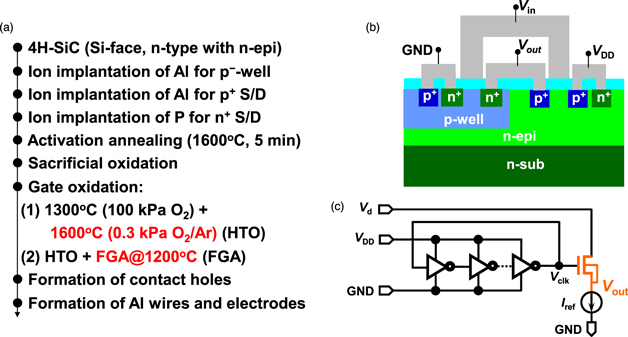
Fig. 1. (Color online) (a) Fabrication process flow of 4H-SiC CMOS inverters and ring oscillators detailing only the major device fabrication steps. (b) Schematic cross-sectional view of fabricated 4H-SiC CMOS inverters along with the biasing arrangement to measure voltage transfer characteristics. (c) Block diagram of a 23-stage ring oscillator and the biasing conditions to evaluate oscillation waveforms.
Download figure:
Standard image High-resolution imagePrior to evaluating the statistic and dynamic performance of the fabricated CMOS circuits, we investigated the discrete n- and p-channel SiC MOSFETs at room temperature. Figure 2(a) shows the normalized drain current versus gate voltage (Id−Vg) characteristics of the HTO and FGA devices, in which Id was normalized by the gate length (L), width (W), and oxide capacitance (Cox) to make a fair comparison. Vd was ±0.1 V for the n- and p-channel devices. Despite the fact that p-channel MOSFETs fabricated by conventional dry oxidation hardly turned on even under large negative Vg conditions (data not shown), the ultrahigh-temperature oxidation and subsequent FGA treatment significantly improved the Id−Vg characteristics, as it did in our previous study. 39) Judging from the distinct positive Vth shift for the FGA p-channel device with respect with the HTO device, it can be concluded that hole trapping at the SiO2/SiC interface, which causes a negative Vth shift, was effectively suppressed. This indicates additional defect passivation with hydrogen through the high-temperature FGA in combination with carbon removal by the ultrahigh-temperature oxidation. Also, as shown in Fig. 2(b), the peak values of μFE estimated from the Id−Vg curves of the p-channel HTO and FGA devices are mostly comparable to the previous results. 39) Regarding the n-channel devices, we have reported a threefold μFE enhancement by ultrahigh-temperature oxidation compared with the conventional dry oxidation. 37) However, the obtained μFE in Fig. 2(b) was below our expectation. As a result, whereas electron mobility in bulk 4H-SiC is much higher than hole mobility, performance of the n-channel MOSFETs is inferior to that of the p-channel one. This is partly due to the higher acceptor density of the p-well region (NA = 5 × 1016 cm−3) in comparison with the previous study (NA = 5 × 1015 cm−3). This implies that the performance of n-channel MOSFETs can be further improved by optimizing the acceptor density for the p-well regions, but careful attention should be paid to designing the p-well regions that requires relatively heavy Al dopant atoms in the development of advanced SiC MOS circuits. Nonetheless, it is notable that well-balanced n- and p-channel MOSFETs with mostly symmetric Vth positions and comparable drivability can be realized with a pure SiO2/SiC interface without interface nitridation by means of the proposed ultrahigh-temperature gate oxidation process.

Fig. 2. (Color online) Performance of discrete n- and p-channel MOSFETs fabricated by HTO and subsequent FGA process: (a) normalized Id−Vg characteristics obtained with Vd of ±0.1 V, (b) μFE plotted against the applied gate voltage. The channel length and width were 100 and 130 μm, respectively. Results from HTO and FGA devices are indicated by the blue and red lines, respectively.
Download figure:
Standard image High-resolution imageFigures 3(a) and 3(b) show voltage transfer curves obtained from the HTO and FGA inverters, in which VDD was varied from 5 to 15 V and Vin was swept from 0 to VDD and back to 0 V. Under the low VDD conditions around 5 V, the HTO device did not exhibit normal inverter operation due to the large ∣Vth∣ for the p-channel MOSFET [less than −10 V as shown in Fig. 2(a)]. When sufficiently high VDD (over 10 V) was applied to the circuit, the full rail-to-rail output signal and sharp switching behavior were observed for the HTO inverter [Fig. 3(a)]. However, the switching threshold voltage, the point on the transfer curve where Vin = Vout, of the HTO inverter shifted toward the low Vin side with respect to the ideal positions (VDD/2) indicated by the vertical dotted lines. In addition, the voltage-transfer characteristics (VTC) showed distinct hysteresis at a high VDD of 15 V. These results are attributable to the relatively large ∣Vth∣ difference between the n- and p-channel HTO MOSFETs [the blue lines in Fig. 2(a)]. In contrast, as shown in Fig. 3(b), the FGA inverter exhibited an ideal threshold voltage (symmetric VTC) and negligible hysteresis under the high VDD condition, thanks to the well-balanced n- and p-channel FGA MOSFETs [the red lines in Figs. 2(a) and 2(b)]. Furthermore, low-VDD operation below 10 V could be achievable for the FGA inverter. These results again demonstrate the effectiveness of combined ultrahigh-temperature oxidation and subsequent high-temperature FGA in reducing carrier trapping at the SiO2/SiC interface.

Fig. 3. (Color online) Voltage transfer curves (Vin−Vout characteristics) of 4H-SiC CMOS inverters obtained with various VDD ranging from 5 to 15 V. Vin was swept from 0 V to VDD and back to 0 V for (a) HTO and (b) FGA inverters. Ideal threshold voltage positions (VDD/2) are indicated with dotted vertical lines in corresponding colors.
Download figure:
Standard image High-resolution imageNext, the dynamic performance of the SiC CMOS inverters was evaluated by analyzing the output oscillation waveforms of the ring oscillators. Figures 4(a) and 4(b) show the output waveforms of the 23-stage ring oscillators fabricated with HTO and FGA inverters, respectively. The waveforms were acquired by continuously applying VDD (15 V) and Vd (5 V) at room temperature. Although the circuits were not fully designed to have ideal oscillation waveforms, stable oscillation signals were observed from both circuits. The FGA circuit exhibited a higher oscillation frequency (shorter delay time) as compared with the HTO one because of the enhanced drivability (Id) and well-balanced Vth for both n- and p-channel MOSFETs due to the effective defect passivation with hydrogen. Moreover, both ring oscillators exhibited stable oscillation in terms of the delay time and waveform for a long period, indicating good immunity against negative and positive bias stresses, as initially expected. The details of the reliability assessment of the inverters and ring oscillators will be described elsewhere.

Fig. 4. (Color online) Output oscillation waveforms of 23-stage 4H-SiC ring oscillators fabricated using (a) HTO and (b) FGA CMOS inverters. The gate length of MOSFETs was 20 μm. The measurements were conducted by applying VDD of 15 V and Vd of 5 V at room temperature. Iref was maintained at −2 mA during measurement.
Download figure:
Standard image High-resolution imageFinally, we investigated the stability of the SiC CMOS inverter and ring oscillators at elevated temperatures. Figures 5(a) and 5(b) show the voltage transfer curves of the HTO and FGA inverters measured at VDD of 15 V. In both cases, the full rail-to-rail output voltage and steep switching behavior were observed even at 200 °C, but the switching threshold voltage shifted toward the lower Vin side, probably due to the asymmetry in Vth between the n- and p-channel MOSFETs. Specifically, whereas the p-channel MOSFETs fabricated by ultrahigh-temperature oxidation and subsequent FGA exhibited a negligible Vth shift up to 200 °C, 39) electron de-trapping from the SiO2/SiC interface resulted in Vth having a significant temperature dependence in the operation of the n-channel MOSFETs. Nevertheless, the FGA inverter is superior to the HTO one in terms of symmetric operation and hysteresis. Consequently, as shown in Fig. 5(c), the FGA circuit showed a shorter propagation delay as compared with the HTO circuit over the whole temperature range. In both cases, a monotonous decrease in the delay time at high temperatures is due to mobility enhancement of n-channel MOSFETs caused by increased mobile electron density. These results indicate the importance of defect passivation at the SiO2/SiC interface for stable SiC circuit operation.

Fig. 5. (Color online) Temperature-dependent characteristics of 4H-SiC CMOS inverters and 23-stage ring oscillators. Voltage transfer curves of discrete (a) HOT and (b) FGA inverters measured at room temperature and 200 °C. (c) Change in propagation delay time estimated from the output oscillation waveforms of HTO (blue) and FGA (red) ring oscillators depending on the measurement temperature. The gate length and supply voltage were 20 μm and 15 V, respectively.
Download figure:
Standard image High-resolution image
In summary, we successfully demonstrated stable operation of SiC CMOS inverters and ring oscillators consisting of non-nitrided MOS structures. High-quality and pure SiO2/SiC interfaces offering superior immunity against bias temperature stressing were fabricated by ultrahigh-temperature oxidation and subsequent FGA treatment. A symmetric and steep rail-to-rail VTC of CMOS inverters was realized with the combined method. Furthermore, the dynamic characteristics of the CMOS inverters were evaluated by performing measurements on 23-stage ring oscillators. The results showed the need for well-balanced and reliable MOSFETs in the development of emerging SiC circuits for harsh-environment applications.
Acknowledgments
This work was partly supported by Adaptable and Seamless Technology Transfer Program through Target-driven R&D (A-STEP) from Japan Science and Technology Agency (JST), Grant Number JPMJTR21R3. The authors would like to thank Professor Tetsuya Hirose and Assistant Professor Takuma Kobayashi of Osaka University for their valuable comments on ring oscillator frequency measurements.