

Abstract
The trends in electronic structure of Bi3+ and Bi2+ as luminescent dopant in wide bandgap inorganic compounds and that of pure Bi-compounds for photocatalytic splitting of water are explored by determination of vacuum referred electron binding energies. Spectroscopic data combined with the chemical shift model from the luminescence field and data on flatband potentials in electrochemistry provide most of the needed data. Occasionally data from photoelectron spectroscopy is used. The trends in VRBE of Bi3+ and Bi2+ ground state and excited state levels resemble that of Ce3+ and Eu2+ lanthanides. To some extend a pure Bi-compound can be regarded as a 100% Bi3+ doped La-compound. This all will be demonstrated and an overview on Bi electronic structure is presented. Comparison of electronic structure for Bi as luminescent dopant in inorganic compounds with pure Bi-compounds entails also a comparison of two disciplines in electro-chemistry, that of luminescence materials and of photo-catalytic compounds.
Export citation and abstract BibTeX RIS

This is an open access article distributed under the terms of the Creative Commons Attribution Non-Commercial No Derivatives 4.0 License (CC BY-NC-ND, http://creativecommons.org/licenses/by-nc-nd/4.0/), which permits non-commercial reuse, distribution, and reproduction in any medium, provided the original work is not changed in any way and is properly cited. For permission for commercial reuse, please email: permissions@ioppublishing.org.
Bismuth as a luminescent activator (Bi2+ or Bi3+) and pure Bi-compounds have a very long history. 1–3 They are being studied for laser applications, phosphors for light emitting diodes (LED), near infrared optical amplifyers, nano-particles for bio-imaging. 4 Bismuth is environmental friendly and non-toxic which is an important criterion for application. Besides luminescence activator, Bi3+ in a wide bandgap compound can also act as a hole trapping and as an electron trapping center, and those aspects can be exploited in afterglow and storage phosphor applications. 5–7 The pure Bi-compounds are studied for photo-catalytic hydrogen production from water. 8 BiVO4 and Bi2O are among the best known examples.3 9,10 Bi4Ge3O14 was discovered in 1973 as scintillation material 11 and today is still widely apllied for detection of γ-ray photons. There is also interest in pure Bi-compounds for photo-voltaic applications, 12,13 battery applications and as a super capacitor for energy storage. 14
How bismuth doped inorganic compounds and pure bismuth compounds perform is intimately connected with the electronic structure. Figure 1a illustrates the principle in photo-catalytic water splitting using a Bi-compound as semi-conducting photo-anode. Valence band (VB) holes and conduction band (CB) electrons are generated by solar light in the photo-anode on the left. Due to band-bending at the anode-water interface, the CB electrons will move to the external circuit and the holes cause a redox reaction with water at the interface to generate the evolution of O2. The electrons via a metal electrode on the right cause a redox reaction leading to the evolution of H2. The bandgap of the photo-anode should be small to absorb large part of the solar spectrum. The electron binding energy at the VB-top at the interface must be below the electrochemical potential for the evolution of O2, and the electron binding energy at the CB-bottom must be above that for the evolution of H2. These potentials are at 0 V and +1.23 V vs the standard hydrogen electrode (SHE) potential which implies at −4.44 eV and −5.67 eV vs the vacuum level. 9,15,16

Figure 1. The role of electron binding energies in Bi-doped and pure Bi-compounds. (a) illustrates the use of Bi-compounds as photo-anode for the generation of hydrogen, (b) illustrates electron trapping in Bi3+ and hole trapping in Bi3+, and the luminescence transitions in Bi3+ and Bi2+. Dashed arrows and levels denote hole transitions and hole states.
Download figure:
Standard image High-resolution imageFigure 1b illustrates the function of Bi3+ and Bi2+ as activator and trapping centers in inorganic wide bandgap compounds. Here, the ground state of Bi3+ is located above the VB-top and its excited state below the CB-bottom. The levels of Bi2+ are located higher in the bandgap and closer to the CB-bottom. Here ground state location actually means the binding energy of an electron in such ground state relative to that at the VB-top. The locations are equivalent to the (Bi3+/Bi4+) and (Bi2+/Bi3+) charge transition levels. If the Fermi level of the compound moves above these charge transition levels, Bi4+ will be reduced first to Bi3+ and next to Bi2+. In the illustration of Fig. 1b, Bi3+ can trap a VB-hole (arrow 1) to become Bi4+ but it also can trap a CB-electron (arrow 2) to become Bi2+. In combination with for example lanthanide based trapping centers, one may design suitable afterglow and charge carrier storage phosphors once the charge transition levels can be predicted. 5,17 Bi3+ and Bi2+ can also act as luminescence centers emitting in the ultraviolet to blue (arrow 3) in the case of Bi3+ and emitting in the deep red (arrow 4) in the case of Bi2+. Bi-luminescence can be quenched by thermal excitation of an electron from the excited state to the empty CB as shown by arrow 5 for Bi3+. Bi3+ emission can also be quenched by thermal excitation of a hole to the VB. In the latter case one may use the hole picture to illustrate hole ionization. 18 In Fig. 1b hole ionisation (arrow 6) is the quenching route since it requires less energy than electron ionization (arrow 5).
This works aims to provide an overview on the electronic structure of pure Bi-compounds and Bi3+ and Bi2+ doped compounds. Due to a lack of a common energy reference such perspective has been hidden or not reckocnized properly. Photo-catalysis is an electrochemical topic where it is customary to use the standard (SHE) or normal hydrogen electrode (NHE) potential as a reference. In the luminescence field, a side-topic of electrochemistry, the energy at the top of the valence band is often used as a reference. However, we are interested in how Bi charge transition levels change with type of compound and using the VB-top as energy of reference will hide such changes. Also the use of different energy references in the different disciplines of electrochemistry prevents the inter-comparison of those fields. To avoid these compound dependent and discipline dependent energy referencing it is essential to use the vacuum level as the common reference for energy.
In the field of luminescence, a method has been developed to determine the binding energies of electrons in impurity and host band states with respect to the vacuum level. 16 The method exploits the unique properties of the 4f-shell of the divalent and trivalent lanthanides. The 4f-shell is being filled with at most 14 electrons in going through the lanthanide series from La to Lu. The shell is located relatively close to the nucleus and surrounded by filled 5s2 and 5p6 orbitals of the atom. There are many different states in the partly filled 4f-shell as given by the famous Dieke level diagram, 19 and transitions between those states provide the lanthanides with their rich, versatile, and excellent luminescence properties that are widely exploited in science and application. The chemical environment interacts with a lanthanide in different ways that will affect the electron binding energies in both the lanthanide and its surrounding anion ligands. We will distinguish three different interactions. (1) The covalence between lanthanide and anion orbitals together with anion polarizability leads to energy lowering of lanthanide electronic states. This is collectively known as the nephelauxetic effect. 20 (2) The low symmetry of a chemical environment, i.e., a crystalline lattice, as compared to the full rotational symmetry of free space, leads to crystal field splitting of otherwise degenerate states. A very important aspect is that inner 4f-orbitals of the lanthanides are rather insensitive to the nephelauxetic effect and crystal field splitting. The Dieke diagram of lanthanide excited states is for that reason almost invariant with type of chemical environment.
There is yet a third interaction (3) which is the chemical shift of binding energy due to the negative screening charge around a cation. The chemical shift of the 4f7 ground state of Eu2+ is about 20 eV in a liquid or solid chemical environment. Most unique is the small compound-to-compound variation in chemical shift. It appears only ±0.3 eV and the variation is also highly predictable from the constituting elements and structure of the compound. What makes lanthanides further unique is the systematics in properties when going through the lanthanide series. The binding in the lanthanide 4fn ground state always follows a similar zigzag pattern as function of n which means that once we know binding energy in one lanthanide we know them for all lanthanides.
In this work we will first briefly address the various methods to determine the binding energies in impurity and host band states with respect to the vacuum level. Next we will briefly review the chemical shift model to determine vacuum referred binding energy schemes from lanthanide spectroscopic data. Then we will apply those models to determine the VRBE energy in bismuth levels when as dopant in a compound and when as a pure Bi-compound. Results from this field of spectroscopy will be compared with that derived from other fields in electrochemistry. We will demonstrate clear systematics with level location or binding energy and the chemical properties of the environment which provides a predictive tool. We will also see that from the binding energy in the Bi3+ and Bi2+ ground states in an inorganic compound one may estimate binding energies in pure Bi-compounds. The overall aim is to provide an overview on how the VRBE in the Bi-levels change with type of compound, and to relate knowledge from the luminescence field with that from photocatalytics.
Methods to Determine Vacuum Referred Electron Binding Energies
The vacuum referred electron binding energy in a multi-electron state of a dopant or at the valence band (VB)-top or conduction band (CB)-bottom is defined as minus the energy needed to remove an electron from such state and bring it to a state where the electron will have zero energy. This is the vacuum level where both kinetic and potential energy is zero. One may distinguish purely experimental methods, semi-empirical methods and computational methods to establish VRBE values.
Experimental and computational methods
A straightforward method to determine vacuum referred binding energies is X-ray or ultraviolet photo-electron spectroscopy (XPS or UPS). Electrons are ejected from occupied states in the sample and their kinetic energy is measured in the vacuum. The methods works well for conducting materials like metals and semi-conductors. However, such method applied to wide bandgap insulators faces problems with sample charging. Contact potentials can also introduce systematic errors. To deal with systematic errors, usually an internal reference is used like the binding at the top of the valence band or the Fermi level in metals. We will use information from photoelectron spectroscopy for a couple of pure Bi-compounds. Unfortunately, the method is not sensitive enough to probe electron binding energies in dopant states when concentrations are in the 1 mole% region.
Flatband potentials are measured by the onset potential for generating photocurrents in semi-conductors. Figure 1a shows CB-bending at the photo-anode water interface. By applying a bias the bending can be reduced to zero (flatband) which then provides information on the energy at the conduction band bottom. For example in Ref. 21 the flatband potential of BiVO4 was determined as −0.58 eV vs the Ag/AgCl redox potential at pH = 6.6. This potential can then be converted to a VRBE at the CB-bottom of −4.49 eV. Subtracting the bandgap energy as determined from a Tauc plot then provides the VB-top at −7.0 eV.
An empirical method frequently encountered in the field of photocatalytic materials is based on the concept of absolute electronegativity of semiconductors. Pearson's 22 or Mulliken's absolute electronegativity of an atom is defined as the arithmatic average of electron affinity and first ionisation potential of that atom. The absolute electronegativity of a semiconductor is then defined as the geometric mean value for the compound, and it defines the mid bandgap VRBE. Meng et al. 23 used that method to determine the VRBE at the CB-bottom and VB-top of bismuth photocatalytic semiconductors. The method is however rather inaccurate. In this work we will see that for pure Bi-compounds it systematically predicts too low VRBEs at the band edges.
Ab-initio and first principle calculations can provide detailed insight in the electronic bandstructure, the wavefunctions of initial and final states in luminescence transitions, and lattice relaxation phenomena. However, calculations still face severe problems when dealing with unoccupied states like that of the conduction band. Bandgaps tend to be largely (30%) under-estimated, and special methods are needed to repair that. At this stage we rate the accuracy of computational methods to establish VRBE energies too poor to be useful for our purpose. What remains as most reliable are the results from the measurement of flatband potentials in electrochemistry and the chemical shift method from lanthanide spectroscopy.
The chemical shift method
A lanthanide VRBE scheme as in Fig. 2 shows the binding energies in the divalent and trivalent lanthanide 4fn states and the lowest energy 4fn-1 5d excited states together with that at the band edges. With the development of the chemical shift model in 2012 16 and its further refinement in 2020 24,25 we are able to construct such schemes routinely with sufficient accuracy to explain and predict many lanthanide luminescence phenomena.
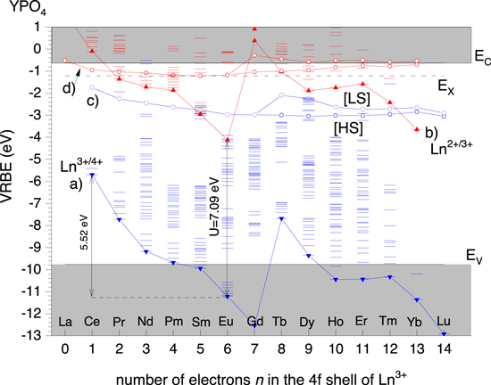
Figure 2. The vacuum referred binding energy scheme for the trivalent and divalent 4fn
lanthanide ground and excited state levels in YPO4. (a) Connects the VRBE in the Ln3+ 4fn
ground state levels and can also be denoted as the (Ln3+/Ln4+) or Ln3+/4+ charge transition levels, (b) connects the same for divalent lanthanides, (c) connects the VRBE in the lowest energy  states of trivalent lanthanides where for
  a distinction between the high spin [HS] and low spin [LS] states is made, (d) connects the same for divalent lanthanides. EV
, EX
, EC
are the VRBE at the valence band top, in the host exciton state, and at the conduction band bottom, respectively.
a distinction between the high spin [HS] and low spin [LS] states is made, (d) connects the same for divalent lanthanides. EV
, EX
, EC
are the VRBE at the valence band top, in the host exciton state, and at the conduction band bottom, respectively.
Download figure:
Standard image High-resolution imageThe main physics behind the chemical shift model is a screening of the positive charge of the lanthanide by the surrounding chemical environment. An Ln2+ will be effectively screened by −2e of negative charge and an Ln3+ by −3e of negative charge. Screening is most optimal in a metal environment where the free conduction band electrons can approach the lanthanide most closely. Screening is least optimal in a fluoride compound where electrons are strongly bonded in the 2p6 fluorine orbitals. In between, screening scales with how strong electrons are bonded in the anion which in turn follows the familiar nephelauxetic sequences, i.e.,  and within the oxides
  aluminates <
  .
20
The Coulomb repulsion between the negative screening charge with an electron in the lanthanide causes a reduction in that electron binding energy. This reduction is called the chemical shift and is by definition zero for the electrons in the free and unscreened lanthanide ions. Equation 1 is the expression from the chemical shift model for the VRBE in the Eu2+ ground state where the second term on the right hand side represents the chemical shift.
24,25
The value of −24.92 eV is the binding in the 4f7 ground state of Eu2+ as free ion and is equivalent to the negative of the 3th ionisation potential of Eu.
.
20
The Coulomb repulsion between the negative screening charge with an electron in the lanthanide causes a reduction in that electron binding energy. This reduction is called the chemical shift and is by definition zero for the electrons in the free and unscreened lanthanide ions. Equation 1 is the expression from the chemical shift model for the VRBE in the Eu2+ ground state where the second term on the right hand side represents the chemical shift.
24,25
The value of −24.92 eV is the binding in the 4f7 ground state of Eu2+ as free ion and is equivalent to the negative of the 3th ionisation potential of Eu.

Over the years YPO4 has served as a model compound to develop, to test, and to refine the chemical shift model, and a diversity of techniques has been applied to obtain data on energy level locations. Figure 2 shows the lanthanide VRBE diagram for YPO4. It was obtained with the refined chemical shift model and the diagram can also be found in Ref. 25. The main parameter is the Coulomb repulsion energy  defined as the electron binding energy difference between the Eu2+ and Eu3+ ground states in chemical environment A. Its value can be deduced from a so-called host referred binding energy (HRBE) diagram derived from lanthanide spectroscopic data. It can also be deduced from the observed centroid shift
  of the Ce3+ 5d-levels in the compound.
26
Equation 1 connects the value for
of the Ce3+ 5d-levels in the compound.
26
Equation 1 connects the value for  with the VRBE
  in the 4f7 ground state of Eu2+ in chemical envrionment A.
  is 18.05 eV for free europium ions and varies from 7.6 eV in highly ionic fluoride compounds (strong anion electron bonding) down to ≈6.0 eV in highly polarizable sulfide and selenide compounds (weak anion electron bonding). The smallest value of about 5.7 eV applies for Eu metal with free conduction band electrons. For YPO4 in Fig. 2 a value of 7.09 eV applies.
In the refined chemical shift model of 2020, the nephelauxetic effect on the binding energy in the lanthanide 4fn
ground state was included. It turns out that the binding energy for  may increase (becomes more negative) several 0.1 eV due to the nephelauxetic effect; the effect for
  is quite insignificant. The schemes and VRBE data presented in this work were all obtained with the refined chemical shift model.
The VRBE in Divalent and Trivalent Bismuth States
Bi3+ has 6s2 ground state electron configuration and the typical energy level scheme is shown in Fig. 3a. Exchange splitting in the excited 6s6p configuration creates an upper 1P spin singlet and lower 3P spin triplet state. The latter is further split by spin orbit interaction. For Bi3+, we traditionally distinguish the spin forbidden A and B-band transitions plus the spin allowed C-band transition.
27
Transitions to 3
P0 are usually too weak to be observed. The wavelength of emission from the 3
P1 level, or A-band emission, varies depending on type of compound from the ultraviolet around 220 nm to the blue around 430 nm. Figure 3b shows the levels of Bi2+ with 6s26p electron configuration. The 2P state is split by spin-orbit interaction, and the  state is further split by the crystal field. The Bi2+ emission is from the
  (1) level and is usually found in the 600–700 nm range.

Figure 3. The level scheme for (a) Bi3+ and (b) Bi2+. The 6s6p excited Bi3+ state is split by the exchange interaction into a 3P and 1P state that are further split by spin-orbit interaction. Spin-orbit interaction in the 6p-orbital of the 6s26p configuration of Bi2+ creates the  ground state and the
  excited state that is further split by the crystal field.
  is the higher energy level of the 6s27s configuration.
Download figure:
Standard image High-resolution imageWe will demonstrate that the VRBE in the Bi3+ ground state or the (Bi3+/Bi4+) charge transition level is located above the VB-top in wide bandgap compounds and the Bi2+ ground state or (Bi2+/Bi3+) charge transition level is found not only below the CB-bottom but also tends to be below the first excited state of Bi3+. This then suggests that in pure Bi-compounds the VB-top will have a strong contribution from Bi3+ ground state orbitals and the CB-bottom from Bi2+ ground state orbitals. To verify this, the VRBE data on pure Bi-compounds will be compared with that of La-compounds and Bi-doped compounds. Clear systematics will appear.
The VRBE in the Bi3+ Dopant Levels
Bi3+ is the preferred valence and has been studied as luminescent center in many types of inorganic compounds. Plenty of information is available on the intrinsic transitions between the 1 S0 ground state and excited states, known as the A, B, and C-band transitions, see Fig. 3 (a). In addition to these intrinsic transitions, also bands attributed to a transition from Bi3+ to the CB is regularly observed which is known as the D-band. With knowledge on the VRBE at the CB-bottom and the D-band energy one may derive the VRBE in the Bi3+ ground state. This method was first employed by Awater and Dorenbos. 28–30 Regarding Bi3+ we can limit here with reviewing and updating the results of that earlier work.
We will start with our model compound YPO4. Blasse et al.
2
already reported in 1968 a broad 3.7 eV emission band with excitation around 5.4 eV. The excitation band was assigned to the Bi3+ A-band in Ref. 31. In 2013 Boutinaud et al.
32
suggested that the 3.7 eV emission might origin from a metal to metal charge transfer (MMCT). One year later, Cavalli et al.
33
extended the studies into the vacuum ultraviolet and reported a broad band between 150 nm and 190 nm that was attributed to the C-band excitation. Again one year later Srivastava et al.
34
assigned the 3.7 eV emission to pairs of Bi3+ in YPO4. Awater and Dorenbos
30
resolved the band between 150 nm and 190 nm into a relatively narrow C-band excitation at 7.9 eV with a broader lower energy band around 7.29 eV which was attributed to the D-band or Bi3+
 CB transition. This D-band can now be used to located the 1
S0 ground state of Bi3+ below the CB. In Fig. 4 we assumed like in Ref. 35 that the VRBE of the electron after D-band excitation falls in between the genuine CB-bottom and EX
. The VRBE in the Bi3+ ground state, or equivalently the (Bi3+/Bi4+) charge transition level, is then at −8.2 V.
CB transition. This D-band can now be used to located the 1
S0 ground state of Bi3+ below the CB. In Fig. 4 we assumed like in Ref. 35 that the VRBE of the electron after D-band excitation falls in between the genuine CB-bottom and EX
. The VRBE in the Bi3+ ground state, or equivalently the (Bi3+/Bi4+) charge transition level, is then at −8.2 V.
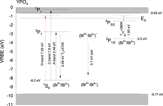
Figure 4. The vacuum referred binding energy scheme for on the left Bi3+ and on the right Bi2+ levels in YPO4. In the middle the levels of Bi-pairs are illustrated.
Download figure:
Standard image High-resolution imageUpon X-ray irradiation of YPO4:Bi3+, a new type of emission appears around 1.85 eV (670 nm) that was attributed to Bi2+ emission. 30 The emission shows a quenching temperature of T50 = 380 K which translates to a quenching energy barrier of about 0.6 eV. Putting things together the Bi2+ ground state or (Bi2+/Bi3+) charge transition level is then estimated at VRBE of −3.5 eV. Note that in Fig. 4 the (Bi2+/Bi3+) charge transition level falls below the VRBE in the 3 P1 excited state of Bi3+. Upon A-band excitation of Bi3+, spontaneous electron transfer to a neigboring Bi3+ to form a Bi4+-Bi2+ pair is then energetically possible. It is now well accepted that the 3.7 eV emission reported already in Ref. 2 originates from Bi-pair emission as suggested in Ref. 34. With the derived charge transition level energies, it becomes clear that Bi3+ forms a 1.57 eV deep trapping center for a hole from the VB and it also forms a ≈2.9 eV deep trapping center for an electron from the CB. The electron and hole trapping properties of Bi3+ together with that of trivalent lanthanides in YPO4, LaPO4, LuPO4 and their solid solutions were studied in Ref. 5 by means of thermo-luminescence and spectroscopic techniques. The results are consistent with the VRBE scheme of Fig. 4. Recently Liu et al. 36 conducted an experimental and theoretical study on charge carrier storage properties of Bi3+ in YPO4. Density Functional Theory (DFT) confirms the location of the charge transition levels above the VB and below the CB. Their calculation also suggest that it is better to speak of a (Bi3+-Bi3+)* excited pair state than in terms of a Bi4+-Bi2+ state. That suggestion was followed in Fig. 4.
Figure 5 shows a stacked VRBE diagram with a compilation of Bi3+ VRBE data in inorganic compounds. Here compounds were selected where data are reasonably reliable and where one may illustrate the trends in level location with type of compound. A quite similar diagram with more compounds can be found in Awater et al.
28,29
In each case the VRBE at the VB-top and CB-bottom is based on lanthanide spectroscopy data combined with the Refined Chemical Shift model. Compounds are in sequence of decreasing value for  .
.

Figure 5. Stacked diagram showing the VRBEs at the VB-top and the CB-bottom together with the VRBE in the Bi3+
1
S0 and 3
P1 states that are connected with the drawn solid curves. The used value for the  parameter is provided at the top of the diagram. If available, the (estimated) location of Bi2+
 ground state and
  (1) excited states are shown. For the indirect bandgap materials SrO, SrS, and CaSe, the VRBE at the CB-bottom pertaining to the direct bandgap is shown.
Download figure:
Standard image High-resolution imageClear trends are observed in Fig. 5. In sequence of decreasing U-value, the polarizability of the anion ligands and its screening potential of the positive Bi3+ cation increases. The chemical shift increases and the VRBE in the Bi3+
1
S0 ground state becomes less negative from values around −11 to −10 eV for U = 7.3–7.4 eV in fluoride compounds to values increasing from −8 eV to −7 eV in oxide compounds with  until finally around −5 eV for CaSe with U = 6.22 eV. The VRBE in the 3
P1 excited Bi3+ state changes then from −5 to −2.5 eV. The excited state VRBE increases therefore less strongly than the ground state VRBE, and as a consequence the energy of the A-band absorption and emission decreases with decreasing U-value.
until finally around −5 eV for CaSe with U = 6.22 eV. The VRBE in the 3
P1 excited Bi3+ state changes then from −5 to −2.5 eV. The excited state VRBE increases therefore less strongly than the ground state VRBE, and as a consequence the energy of the A-band absorption and emission decreases with decreasing U-value.
Figure 6 compiles data on the A-band absorption energy against the U-value assigned to the compound. A clear trend is revealed that confirms a long known observation that the A-band energy lowers with increasing nephelauxetic effect.
1,2
In other words it scales with how strong electrons are bonded in the anions and therefore with the  value of the chemical shift model. Data on Bi3+ in GdOCl, LaOBr, YOCl, and LaOCl are outlyers in Fig. 6 which may suggest that either improper assignments have been made or that specific compound properties are at play; this needs further analysis.
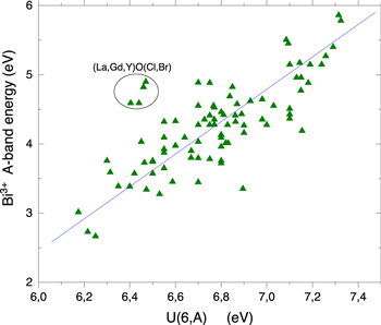
Figure 6. The energy of the Bi3+ A-band energy in compounds observed in absorption or in excitation spectra against the  value assigned to that compound.
Download figure:
Standard image High-resolution imageThe VRBE in the Bi2+ dopant levels
Bi3+ is the preferred valence in inorganic compounds but also Bi2+ can be stable although information is much less abundant. The Bi2+ emission is usually found in the 550–720 nm spectral region. 37–39 Interest in Bi2+ has increased because of potential phosphor application in white-LEDs, and there is also active research in afterglow and storage phosphor applications where Bi3+ may act as a stable electron trapping and/or hole trapping center 5,17,40,41 as illustrated in Fig. 1b.
Various methods to determine or estimate the VRBE in the  ground state and emitting
  excited state of Bi2+ were used in Ref. 29. For a couple of compounds one can use information on energy of electron transfer from Bi2+ to the CB-bottom or from the VB-top to Bi3+. However, very little information appears available. The presence of Bi2+ emission and the quenching temperature of that emission also provides information on excited state level location with respect to the CB-bottom. Information on the VRBE in Bi2+ levels has been compiled in the stacked diagram of Fig. 7.
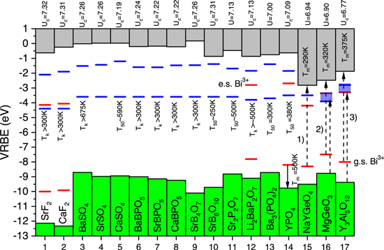
Figure 7. Stacked diagram showing the VRBEs at the VB-top and the CB-bottom together with Bi2+ level locations (in blue), and when available also Bi3+ levels (in red). The  parameter is provided at the top of the diagram. Luminescence quenching temperatures Tk
and T50 are provided.
parameter is provided at the top of the diagram. Luminescence quenching temperatures Tk
and T50 are provided.
Download figure:
Standard image High-resolution imageFor the compounds 1 until 14, Bi2+ emission and its excitation spectra have been reported.
29
The approximate VRBE energies in the  excited state were deduced from the thermal quenching temperature T50 or the onset of thermal quenching Tk
of the Bi2+ emission. We regard the thermal ionization to the conduction band as the quenching mechanism, and with a typical lifetime of 10–20 μs
39,42–44
roughly 600 K eV−1 change in T50 is assumed. The relatively low quenching temperature of T50 = 250 K in SrB6O10 then translates to a
excited state were deduced from the thermal quenching temperature T50 or the onset of thermal quenching Tk
of the Bi2+ emission. We regard the thermal ionization to the conduction band as the quenching mechanism, and with a typical lifetime of 10–20 μs
39,42–44
roughly 600 K eV−1 change in T50 is assumed. The relatively low quenching temperature of T50 = 250 K in SrB6O10 then translates to a  location less than 0.5 eV below the CB-bottom. T50 values are also known for CaSO4, Sr2P2O7, Ba3(PO4)2, and YPO4 (see Fig. 4). In each case, a VRBE in the Bi2+ ground state is found around −3.6 eV, and similar values for compounds where only a lower limit for Tk
is available was assumed.
location less than 0.5 eV below the CB-bottom. T50 values are also known for CaSO4, Sr2P2O7, Ba3(PO4)2, and YPO4 (see Fig. 4). In each case, a VRBE in the Bi2+ ground state is found around −3.6 eV, and similar values for compounds where only a lower limit for Tk
is available was assumed.
The data on YPO4 (compound 14) are the same as in Fig. 2 and Fig. 4. The last three compounds NaYGeO4, MgGeO3 and Y3Al5O12 in Fig. 7 have relatively low VRBE at the CB-bottom, i.e. <−2 eV, and no Bi2+ emission is observed. Evidently the  excited state is located inside the CB. For these compounds Bi2+ VRBE values can be estimated from thermoluminescence data on Bi3+ (co)-doped compounds. Bi3+ acting as an electron trapping center was studied in NaYGeO4 by Lyu et al.,
17
in MgGeO3 by Katayama et al.,
41
and in Y3Al5O12 by Katayama et al.
40
For example in Bi3+ doped NaYGeO4 a glow peak at ≈290 K has been assigned to electron release from Bi2+
17
and this translates to a Bi2+ g.s. location about 0.6 eV below the CB-bottom as in Fig. 7. The glow peak appears at 320 K in MgGeO3 and at 375 K in Y3Al5O12. Dashed arrows (1), (2), (3) are observed charge transfer bands. Arrow 1) of length 5.34 eV was assigned to the Bi3+
excited state is located inside the CB. For these compounds Bi2+ VRBE values can be estimated from thermoluminescence data on Bi3+ (co)-doped compounds. Bi3+ acting as an electron trapping center was studied in NaYGeO4 by Lyu et al.,
17
in MgGeO3 by Katayama et al.,
41
and in Y3Al5O12 by Katayama et al.
40
For example in Bi3+ doped NaYGeO4 a glow peak at ≈290 K has been assigned to electron release from Bi2+
17
and this translates to a Bi2+ g.s. location about 0.6 eV below the CB-bottom as in Fig. 7. The glow peak appears at 320 K in MgGeO3 and at 375 K in Y3Al5O12. Dashed arrows (1), (2), (3) are observed charge transfer bands. Arrow 1) of length 5.34 eV was assigned to the Bi3+
 CB transition and provides the Bi3+ VRBE.
17
The charge transfer band at 4.86 eV (arrow 2) in MgGeO3 from Ref. 41 was assigned to the Bi3+
CB transition and provides the Bi3+ VRBE.
17
The charge transfer band at 4.86 eV (arrow 2) in MgGeO3 from Ref. 41 was assigned to the Bi3+
 CB transition. However, one may not fully exclude that it is the VB
  Bi3+ CT, and both options are illustrated in Fig. 7. Similar applies to the 5.93 eV (arrow 3) CT-band in Y3Al5O12 from Ref. 45 that was assigned to the Bi3+
 CB transition in Ref. 28. The other option is also shown in Fig. 7. This ilustrates that depending on level locations in the bandgap a proper assignment of broad CT-bands becomes difficult or ambiguous.
Thermoluminescence can also be used to determine the VRBE in the Bi3+ ground state. In Eu3+ and Bi3+ co-doped YPO4, Eu3+ appears to be a deeper electron trap than the hole trap depth of Bi3+. During TL-readout the hole is released from Bi4+ to recombine with the electron trapped on Eu2+ to generate Eu3+ emission apearing as a TL-glow peak around Tm = 500 K. 5 With such information we can then estimate that the VRBE in the Bi3+ ground state must be at least 1 eV above the VB-top which is then consistent with Fig. 4.
Figure 7 shows that the VRBE in the Bi2+ ground state is fairly constant with values (tentatively) slighty below 4 eV in fluoride compounds to values around −3.6 eV in more polarizable oxide compounds. Comparing Fig. 5 with Fig. 7 one may notice that, at a given U-value, the VRBE in the Bi2+ ground state tends to fall below the VRBE in the Bi3+ excited state. This was clearly illustrated for Bi2+ and Bi3+ in YPO4 in Fig. 4. This confirms again that when two Bi3+ dopants are close together and one of them is brought to the excited state, a lower energy (Bi3+-Bi3+)* excited pair state may form. The electron back transfer may then generate so called Bi-pair emission or, in case the back transfer is radiationless, form a concentration quenching route for ordinary Bi3+ A-band emission as suggested in Awater et al. 29
The VRBE in Pure Bi-compounds
The obtained data on pure Bi-compounds are presented as a stacked VRBE diagram in Fig. 8. Here a distinction is made between a definition of CB-bottom in semi-conducting compounds and in wide bandgap luminescent compounds. In the former, the optical bandgap or fundamental absorption threshold Efa
is obtained from a Tauc plot. Efa
then defines the location of the CB-bottom above the VB-top. In wide bandgap compounds like YPO4 in Fig. 2, Efa
is often followed by a distinct excitation peak at Eex
due to host exciton creation. This defines EX
in Fig. 2. Since an exciton is a bound electron-hole pair we still need to add the exciton binding energy  to reach the mobility edge defined as the CB-bottom EC
in VRBE diagrams. The empirical relation
to reach the mobility edge defined as the CB-bottom EC
in VRBE diagrams. The empirical relation

has been used. 46 For ≈3 eV bandgap semi-conductors, the bonding is about 0.1 eV and one may expect that at room temperature exciton dissociation generates already free charge carriers. For ≈10 eV wide bandgap compounds binding energies increase toward 1 eV, and excitation at Efa does not create free charge carriers.
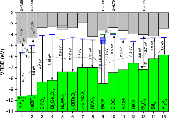
Figure 8. Stacked VRBE scheme for pure Bi-compounds. The horizontal bars (blue) connected with a dotted curve in the bandgap represent the flatband potentials. Occasionally relevant levels of Tb3+, Eu2+ and Pr3+ are shown (green). In case of downward pointing arrows, the VRBE at the VB-top is derived from the measured flatband. In case of upward pointing arrows, the flatband was derived from the VB-top. The dashed curve connects the VRBE at mid bandgap energy as predicted from the absolute semiconductor electronegativity.
Download figure:
Standard image High-resolution imageSpectroscopic information on lanthanides in pure Bi-compounds is too rare to routinely derive the VRBE at the VB-top and CB-bottom with the chemical shift method, and we need data from other methods. The electrochemical determination of the flatband potential is regarded as the best alternative. By subtracting the value for Efa from the flatband potential, the VRBE at the VB-top is obtained. Figure 8 shows the measured or derived flatband potentials on the VRBE scale as horizontal levels connected by a dotted curve. Down pointing arrows show how the VB-top is reached using measured values for Efa . By adding the energy where optical absorption is maximum, EX is reached and with Eq. 2 EC is finally obtained. Those EC values are used in Fig. 8. Note that they are related to the direct bandgap whereas Efa can be from the indirect bandgap. It is realized that the maximum in optical absorption not necessarily corresponds with Eex and then EC may not represent the genuine mobility edge of the compounds, but at the moment this seems the best approach we can take. In the end it is not that essential for the conclusions of this work. An account on how data were obtained for each individual compound in Fig. 8 is provided below.
Data used for the pure Bi-compounds
Fluorides. The VRBE of −9.6 eV at the VB-top of BiF3 is from X-ray photoelectron spectroscopy (XPS).
47
Information on  and
and  from Refs. 48, 49 was used to estimate the flatband potential and EC
. Figure 8 shows for BiF3 the 5
D4 excited state of Tb3+ at −5.77 eV. The emission from this state has a reported quenching temperature of T50 ≈ 300 K.
49
In Ref. 18 such quenching temperature was related to an energy difference with
from Refs. 48, 49 was used to estimate the flatband potential and EC
. Figure 8 shows for BiF3 the 5
D4 excited state of Tb3+ at −5.77 eV. The emission from this state has a reported quenching temperature of T50 ≈ 300 K.
49
In Ref. 18 such quenching temperature was related to an energy difference with  . We thus estimate
  which is fully consistent. For NaBiF4, with 5
D4 level at −5.66 eV and luminescence quenching temperature T50 = 450 K from Ref. 49 one obtains
which is fully consistent. For NaBiF4, with 5
D4 level at −5.66 eV and luminescence quenching temperature T50 = 450 K from Ref. 49 one obtains  . Further, with
  and Efa
= 4.5 eV,
49,50
the VRBE at the VB-top at −9.5 eV and the flatband potential at −5 eV is derived.
and Efa
= 4.5 eV,
49,50
the VRBE at the VB-top at −9.5 eV and the flatband potential at −5 eV is derived.
Oxides. For the monoclinic phase of BiPO4, a flatband potential of −4.1 eV is from Refs. 51, 52 and with  and
and  ,
52,53
EV
and EC
were obtained. The VRBEs in the host bands of Bi4Ge3O12 are an educated guess where we assumed a flatband potential of −4 eV which is typical for other Bi-compounds in Fig. 8. Subtracting Efa
= 4.16 eV from Ref. 54 assigned to the indirect bandgap provides EV
= −8.16 eV. The optically determined
,
52,53
EV
and EC
were obtained. The VRBEs in the host bands of Bi4Ge3O12 are an educated guess where we assumed a flatband potential of −4 eV which is typical for other Bi-compounds in Fig. 8. Subtracting Efa
= 4.16 eV from Ref. 54 assigned to the indirect bandgap provides EV
= −8.16 eV. The optically determined  then provides EC
.
55,56
then provides EC
.
55,56
Transition metal compounds. For Bi2WO6, the flatband potential of −4.48 eV and Efa
= 2.9 eV were used.
57
Reports on the maximum of the absorbance vary from 3.7 eV in Refs. 58, 59 to 4.1 eV in Refs. 57, 60, 61 which gives uncertainty in Eex
and where to locate EC
; a value of 3.9 ± 0.2 eV was used. For the triclinic β-BiTaO4 phase we used the flatband potential of −4.22 eV and Efa
= 3.18 eV from Ref. 62 to derive EV
, and with  to derive EC
.
63–65
For the α-BiNbO4 phase we used a flatband potential of ≈−4.4 eV and Efa
= 2.6 eV to obtain EV
.
66
With
to derive EC
.
63–65
For the α-BiNbO4 phase we used a flatband potential of ≈−4.4 eV and Efa
= 2.6 eV to obtain EV
.
66
With  , EC
is found.
63,67
For monoclinic phase BiVO4 we used the flatband potential of −4.49 eV and Efa
= 2.51 eV from Ref. 21 to determine EV
and
, EC
is found.
63,67
For monoclinic phase BiVO4 we used the flatband potential of −4.49 eV and Efa
= 2.51 eV from Ref. 21 to determine EV
and  from Refs. 68, 69 to determine EC
.
from Refs. 68, 69 to determine EC
.
Halo-oxides. For the halo-oxide family information on electrochemical flatband determination was not found, and other methods were followed to deduce them. For BiOF with  , the (Eu2+/Eu3+) charge transition level is at −3.97 eV. The
  charge transfer band is at 4.49 eV,
70
and then EV
= −8.46 eV. The host absorption maximum is seen at 4.88 eV in Ref. 71 and at 4.63 eV in Ref. 72 yielding EX
≈ −3.8 eV. In Ref. 73 a VB-top at −8.39 eV was suggested to explain the mechanism of photocatalytic activity. With computational methods the VB-top is found at −8.2 eV.
74
Considering systematic errors of several 0.1 eV in each method used, the VRBE at the VB-top appears consistent. To estimate the flatband potential, Efa
needs to be added to EV
= −8.46 eV. Experimental values of 3.6 eV and 4.2 eV have been reported.
72,73,76
A computed value of 4.2 eV is reported in Ganose et al.
74
We estimate a flatband potential somewhere around −4.5 ± 0.3 eV.
charge transfer band is at 4.49 eV,
70
and then EV
= −8.46 eV. The host absorption maximum is seen at 4.88 eV in Ref. 71 and at 4.63 eV in Ref. 72 yielding EX
≈ −3.8 eV. In Ref. 73 a VB-top at −8.39 eV was suggested to explain the mechanism of photocatalytic activity. With computational methods the VB-top is found at −8.2 eV.
74
Considering systematic errors of several 0.1 eV in each method used, the VRBE at the VB-top appears consistent. To estimate the flatband potential, Efa
needs to be added to EV
= −8.46 eV. Experimental values of 3.6 eV and 4.2 eV have been reported.
72,73,76
A computed value of 4.2 eV is reported in Ganose et al.
74
We estimate a flatband potential somewhere around −4.5 ± 0.3 eV.
For BiOCl, Efa
= 3.5 eV and  are reported.
75–77
Information on flatband potential studies was not found and the VRBE was derived from lanthanide spectroscopy instead. The (Eu2+/Eu3+) charge transition level when
are reported.
75–77
Information on flatband potential studies was not found and the VRBE was derived from lanthanide spectroscopy instead. The (Eu2+/Eu3+) charge transition level when  is at −3.92 eV, and with a
  CT band reported near 3.55 eV
75,78,79
the VB-top is reached at −7.47 eV. Adding Efa
, a flatband potential around −3.97 eV is expected.
CT band reported near 3.55 eV
75,78,79
the VB-top is reached at −7.47 eV. Adding Efa
, a flatband potential around −3.97 eV is expected.
For BiOBr, experimental information on lanthanide spectroscopy and flatband studies are not available. From the absolute semiconductor electronegativity, the mid bandgap VRBE is calculated at −6.1 eV.
23,80
With  and
and  ,
79–82
the VB-top would be at −7.5 eV, the flatband at −4.7 eV, and EC
at −3.9 eV. However, as will be shown later absolute semiconductor electronegativity systematically provides too low values for the band positions in pure Bi-compounds. We tentatively assumed 0.3 eV higher values which locates the flatband at −4.4 eV.
,
79–82
the VB-top would be at −7.5 eV, the flatband at −4.7 eV, and EC
at −3.9 eV. However, as will be shown later absolute semiconductor electronegativity systematically provides too low values for the band positions in pure Bi-compounds. We tentatively assumed 0.3 eV higher values which locates the flatband at −4.4 eV.
For BiOI, we followed the same method as for BiOBr. The concept of absolute semiconductor electronegativity used in Refs. 23, 83 yields the mid bandgap VRBE at −5.94 eV. With  from Refs. 80, 84, 85 and Efa
= 1.94 eV from Refs. 80, 83, 84, one obtains EV
= −6.85 eV, a flatband at −4.9 eV, and EC
at −4 eV. These values are quite similar to that of computational studies in Ganose et al.
74
providing EV
= −7 eV and a flatband at −5 eV. Yet, because of the systematic error, we will place the band edges at 0.25 eV higher energy bringing the flatband at −4.65 eV.
from Refs. 80, 84, 85 and Efa
= 1.94 eV from Refs. 80, 83, 84, one obtains EV
= −6.85 eV, a flatband at −4.9 eV, and EC
at −4 eV. These values are quite similar to that of computational studies in Ganose et al.
74
providing EV
= −7 eV and a flatband at −5 eV. Yet, because of the systematic error, we will place the band edges at 0.25 eV higher energy bringing the flatband at −4.65 eV.
BiI3
, Bi2
O3
and Bi2
S3
. For BiI3, a workfunction of 5.8 eV as obtained from photoelectric effect measurements suggest EV
= −5.8 eV.
86
UPS studies indicate EV
between −6 and −6.3 eV.
13
A strong exciton peak at  is reported in Refs. 87– 89 with direct bandgap of 1.96 eV and indirect bandgap of 1.67 eV.
88
Altogether we used
is reported in Refs. 87– 89 with direct bandgap of 1.96 eV and indirect bandgap of 1.67 eV.
88
Altogether we used  , a flatband near −4.3 eV and EC
near −4.1 eV in Fig. 8 as compromise between the different sets of data.
, a flatband near −4.3 eV and EC
near −4.1 eV in Fig. 8 as compromise between the different sets of data.
Bi2O3 is well-studied for photo-catalytic purposes
90–92
with a measured flatband potential of −4.37 eV.
90
With  and Efa
= 2.8 eV,
and Efa
= 2.8 eV,  is obtained.
90,92–94
We can also exploit data on Pr3+ in Bi2O3. Pr3+ creates a broad unresolved diffuse reflectance band extending from 425 nm (2.9 eV) to 525 nm (2.4 eV)
94
that we here attribute to the Pr
is obtained.
90,92–94
We can also exploit data on Pr3+ in Bi2O3. Pr3+ creates a broad unresolved diffuse reflectance band extending from 425 nm (2.9 eV) to 525 nm (2.4 eV)
94
that we here attribute to the Pr intervalence charge transfer (IVCT) band. With the (
 ) charge transition level at −6.88 eV for
  = 6.55 eV this is fully consistent with the VRBE data in Fig. 8.
Bi2S3 has a measured flatband potential of −4.26 eV.
90
With  and Efa
= 1.6 eV,
95,95–97
EV
= −5.86 eV and EC
= −3.4 eV are obtained.
and Efa
= 1.6 eV,
95,95–97
EV
= −5.86 eV and EC
= −3.4 eV are obtained.
A first inspection of Fig. 8 shows that the flatband potentials are fairly constant and usually fall between −4 and −4.5 eV. For the two fluoride compounds they are 1 eV lower. For each compound in Fig. 8, the VRBE at mid bandgap was also calculated from the absolute semiconductor electronegativity, see also, 23 and the values are connected by the dashed line. In all cases it runs significantly below the mid bandgap energy as derived experimentally. Clearly there appears to be a systematic difference which raises doubts on the validity of the frequent use of absolute semiconductor electronegativity in the field of photocatalytic compounds. For compounds where information on lanthanide spectroscopy combined with the chemical shift model has been used, results are consistent with experimental flatband determinations.
Equivalent La-based compounds
Bi3+ has similar ionic radius and charge as La3+ and also the crystal structure of a pure Bi-compound is usually similar to that of the equivalent La-compound. It is then of interest to compare the VRBE in the pure Bi-compounds of Fig. 8 with that of La-compounds as shown in 9. Since there is no equivalent La-compound for Bi4Ge3O12 we used information on LaAlGe2O7 instead. Lanthanide spectroscopy on La2WO6 appears too scarce, and instead we used Y2WO6 as equivalent compound for Bi2WO6 in Fig. 9. The standard method of the (refined) chemical shift model was used to construct the lanthanide VRBE diagrams. The two fluorides are 11 eV wide bandgap compounds. The VB-top in the oxide and halo-oxide compounds are found in the −8 eV to −9 eV region, and that of LaI3 and La2S3 at 3 eV higher energy. Note the relatively low lying CB-bottom in the four transition metal based compounds which is dominated by the VRBE in the 5d (W5+ and Ta4+), 4d (Nb4+), and 3d (V4+) orbitals. 98 Germanium based compounds, as in LaAlGe2O7 also tend to have low lying CB-bottom.
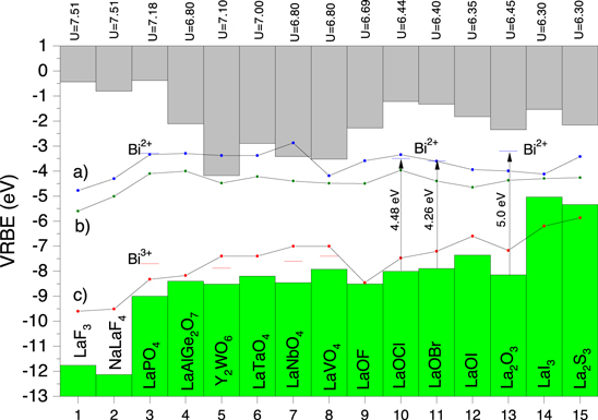
Figure 9. Stacked diagram showing the VRBEs at the VB-top and the CB-bottom of La-based compounds and of Y2WO6. For several compounds the (Bi3+/Bi4+) and (Bi2+/Bi3+) charge transition levels are shown. Solid curves a), b), and c) connect the VRBE at the CB-bottom, of the flatband potential, and VB-top of corresponding pure Bi-compounds, respectively.
Download figure:
Standard image High-resolution imageFor several of the La-compounds and for Y2WO6, spectroscopic data on Bi3+ is available enabling to determine or estimate the VRBE in the Bi3+ and Bi2+ impurity ground states. Bi data for LaPO4 can be found in Ref. 5 for Y2WO6 in Refs. 2, 28, 99, for LaNbO4 in Refs. 28, 100, for LaVO4 in Refs. 28, 101. For LaOBr we interpreted a broad 4.26 eV excitation band for Bi emission
102
as the VB  Bi3+ CT-band. Similar was done for the 4.48 eV excitation band in Bi3+ doped LaOCl in Ref. 103 and for the 5.0 eV band in La2O3 from Refs. 104, 105. The interpretation of the broad bands in these latter three compounds remains speculative. The alternative interpretation of a Bi3+
 CB or a broad band (Bi3+-Bi3+) pair excitation cannot be excluded at this stage.
In Fig. 9 the VRBE of the CB-bottom, flatband potential, and VB-top of the corresponding pure Bi-compounds of Fig. 8 are connected by curves a), b), and c), respectively. Curve c) tends to follow the same patterns as the VRBE at the VB-top of the La-compounds whereas the flatband potential is fairly constant around −4 eV without a correlation with the CB-bottom of the La-compounds.
Discussion
In discussing the trends in VRBE in the Bi3+ and Bi2+ ground and excited states we will compare the observations with trends known for the lanthanides Ce3+ and Eu2+ that have about similar ionic radius as Bi3+ and Bi2+. An important difference is the localized and atomic character of the inner 4f-oribital that is occupied with one or seven electrons in the ground states of Ce3+ or Eu2+. The VRBE in the lanthanide 4fn
ground states is very little affected by crystal field splitting and the nephelauxetic effect. The remaining compound dependent effect is the chemical shift. Equation 1 is the expression for the VRBE in the Eu2+ ground state. Subtracting  and adding the VRBE difference
  between Ce3+ and Eu3+ one obtains the VRBE
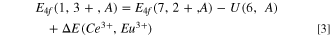
  in the Ce3+ ground state as in Eqs. 3 and 4. That difference is 5.52 eV in Fig. 2 and does not significantly change with type of compound.

The VRBE in the 4f ground state of Ce3+ as free ion is −36.9 eV, and with  increasing from 7.6 eV toward 6.2 eV that VRBE increases from −6.40 eV toward −4.33 eV as shown with curve a) in Fig. 10. The VRBE in the Bi3+ 6s2 ground state as free ion is equivalent to the negative of the 4th ionisation potential of bismuth and equals −45.4 eV. Figure 5 shows that in compounds the Bi3+ VRBE increases from −11 eV in BaF2 up to near −5 eV in CaSe. It appears thus that the chemical shift in absolute number (≈34 eV) and its increase of ≈6 eV with decreasing U-value is somewhat larger than the values of ≈31 eV and 2.5 eV for Ce3+. Nevertheless the upward trend is precisely the same and follows the nephelauxetic sequence. The stronger trend for Bi3+ may be related with a stronger interaction of the outer 6s2 orbital with the anion screening charge as compared with that of the inner 4f-orbital, and supposedly also covalence with the anion ligands will be more strong.

Figure 10. The VRBE in the (curve a) Ce3+ and in the (curve b) Eu2+ 4f ground state. Solid data symbols are the VRBE in the lowest energy Ce3+ 5d state with compound average VRBE of −1.6 eV, and open symbols in the lowest energy 4f65d state of Eu2+ with compound average VRBE of −1.1 eV. Data on 225 compounds were used.
Download figure:
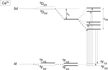
Standard image High-resolution imageLet us now turn to the VRBE in the 3
P1 excited Bi3+ state and compare that with the VRBE in the lowest energy excited 5d state of Ce3+. The 5d-orbital extends to the outside of the Ce3+ cation and besides chemical shift it is also subject to crystal field splitting and nephelauxetic effect as illustrated in Fig. 11. The nephelauxetic effect, is responsible for the so-called centroid shift  of 5d-energy.
26
The increase of centroid shift with decreasing
of 5d-energy.
26
The increase of centroid shift with decreasing  is about the same as the increase of chemical shift, and as a result the average VRBE of the five 5d-levels appears almost invariant with type of compound. This means that the compound to compound variation in the VRBE in the lowest energy 5d-level shown with the data in Fig. 10 is caused by compound-to-compound variation in the 5d crystal field splitting
  .
.
Figure 11. The level scheme for Ce3+. The spin orbit split 2D levels of Ce3+ are lowered by the centroid shift  and depending on site symmetry split into at most five 5d levels.
  is the differnce between lowest and highest energy 5d level.
Download figure:
Standard image High-resolution image
Clearly for Bi3+, both the 6s2 ground state and 6s6p excited state orbitals extend to the outside of the cation and both will have strong interaction with the anion ligands which makes VRBE interpretation more complex than with Ce3+. Figure 5 shows that the VRBE in the 3
P1 excited state increases less strongly then that in the 1
S0 ground state when  decreases. The A-band energy decreases as shown in Fig. 6, and this is the same trend as can be seen in Fig. 10 for the energy difference between the Ce3+ ground state (curve a) and the lowest energy 5d-state (solid data symbols).
The VRBE in the 6s26p ground state of the free ion Bi2+ is −25.5 eV and this is almost the same as −24.92 eV for Eu2+ (see Eq. 1). Figure 7 shows that in compounds the Bi2+ ground state VRBE is found around −4 to −3.5 eV and this is at most a few 0.1 eV above that for Eu2+ in Fig. 10. The variation in ground state VRBE with  -value is like curve b) in Fig. 10 for Eu2+ rather mild. Unlike the A-band of Bi3+ there appears no decreasing trend in energy difference between ground and excited Bi2+ states with decreasing U-value. This suggests that compound-to-compound variations are related with changing crystal field splitting and spin orbit splitting of the Bi2+ levels, see also Fig. 3. Data are actually too few to enter into a detailed discussion on the relation between structure and chemistry of compounds and the wavelength of Bi2+ emission.
In Fig. 5, the VRBE in the Bi3+ ground state appears always above the top of the VB formed by the anion. Extrapolating toward 100% Bi3+ concentration suggests that the top of the VB in pure Bi-compounds will largely be determined by the Bi3+ 6s2 cation orbitals rather than the anion orbitals. Indeed the VRBE at the VB-top in the pure Bi-compounds of Fig. 8 appears at similar energy as that in the Bi3+ ground state in Bi3+ doped compounds in Fig 5. With decreasing U-value it decreases from just above −10 eV in BiF3 to around −6 eV in CaSe. The flatband potential of the pure Bi-compounds in Fig. 8 is always near −4 eV and this is then consistent with the VRBE of around −3.6 eV in the ground state of Bi2+ as dopant in the compounds of Fig. 7.
The La-compounds in Fig. 9 are, when doped with 100% Bi3+, regarded to be similar as the Bi-compounds in 8. Curve c) in Fig. 9 connects the VRBE at the VB-top of those Bi-compounds. For the oxide and halooxide compounds, curve c) runs close above the VB-top which suggest that the VB-top in the equivalent Bi-compound is likely to be of mixed cation anion orbital character. For the two fluoride compounds there is about 2 eV difference which then suggest that the VB-top in the fluorides is dominated by the Bi3+ ground state orbitals. In LaI3 and La2S3 the situation is reversed. This suggests that Bi increases the bonding in the anion thus lowering EV . Computational methods can provide more detailed insight. Curve b) representing the flatband potentials and curve c) in Fig. 9 is usually well below the CB-bottom of the La-compounds and then the CB-bottom in the Bi-compound will be formed by Bi2+ orbitals. However in case of Y2WO6, LaTaO4, LaNbO4, and LaVO4 we deal with a low lying CB-bottom formed by the transition metal d-orbital states. Curve b) is now close to that CB-bottom, and the CB-bottom is likely of mixed Bi2+ 6s26p and transition metal d-orbital type. Indeed computational methods show that the CB-bottom in BiVO4 and also Bi2WO6 is dominated by V4+ 3d and W5+ 5d-orbitals. 10,61,106
The parameter  is the energy difference between the (Eu2+/Eu3+) and (Eu3+/Eu4+) charge transition levels and varies from 7.6 eV down to 6.0 eV in a predictable fashion. One may compare this with the energy difference UBi
between the (Bi2+/Bi3+) and (Bi3+/Bi4+) charge transition levels. Figure 8 suggest about 4.5 eV for fluorides compounds, 3.7 eV in YPO4 in Fig. 4, and 2.8 eV for Bi2O3 in Fig. 8 and possibly even lower values in sulfide and selenide compounds. The trends are the same as with
is the energy difference between the (Eu2+/Eu3+) and (Eu3+/Eu4+) charge transition levels and varies from 7.6 eV down to 6.0 eV in a predictable fashion. One may compare this with the energy difference UBi
between the (Bi2+/Bi3+) and (Bi3+/Bi4+) charge transition levels. Figure 8 suggest about 4.5 eV for fluorides compounds, 3.7 eV in YPO4 in Fig. 4, and 2.8 eV for Bi2O3 in Fig. 8 and possibly even lower values in sulfide and selenide compounds. The trends are the same as with  .
.
The interpretation of the spectroscopy of Bi3+ in compounds has always been difficult and controversial, and it often still is. Special about Bi is that both the (Bi3+/Bi4+) and (Bi2+/Bi3+) charge transition levels are found inside the forbidden gap of wide band insulators. Furthermore the Bi3+ excited state is usually above and in any case near the Bi2+ ground state. One may then in principle observe three broad electron transfer bands in a Bi3+ doped compound, i.e., the VB  Bi3+ electron transfer band, the Bi3+
 CB electron transfer band and, when Bi3+ ions are nearest neighbors, the Bi3+
 Bi3+ electron transfer band. Each electron transfer can be followed by broad band charge transfer emission. Without detailed knowledge on the location of the charge transition levels, assignment of the broad bands remains speculative. The quenching of Bi3+ emission may proceed via thermal ionization of an electron to the CB but also by thermal ionization of a hole to the VB, see Fig. 3 and again the location of the charge transition levels is detremental for which quenching route prevails.
Conclusions
The chemical shift method of VRBE scheme construction combined with spectroscopy on Bi3+ and Bi2+ enables to derive the electron VRBE in the divalent and trivalent Bi-levels. When compounds are organized in order of decreasing  -value, which means increasing nephelauxetic effect, increasing polarizability of the anions, and increasing co-valence, clear systematics appear as shown in Fig. 5 and Fig. 7. Just like Ce3+, the ground state VRBE increases with smaller value for U. A smaller cation charge leads to less dependence of VRBE on type of compound. This is known for Eu2+ as compared to Ce3+ as can be seen in Fig. 10, but this work confirms the same for Bi2+ compared to Bi3+. One may then roughly estimate the VRBE energies in the Bi2+ and Bi3+ ground states from the composition of the compound beforehand. In lanthanides the 4f-orbital is shielded and electron VRBE is hardly affected by the nephelauxetic effect and crystal field splitting. This is different for bismuth where the 6s2 and 6s26p orbital extends to the outside of the atom and more compound-to-compound variation in Bi ground state VRBE results.
This work also shows that knowledge on the VRBE in Bi doped compounds can be transferred to pure Bi-compounds. Here we see in Fig. 8 the same systematics. The VB-top raises with smaller U-value like the Bi3+ ground state VRBE in Fig. 5 and the flatband potential is fairly constant −4 to −3.5 eV just like that of the Bi2+ ground state VRBE in Fig. 7. Transition metals like V5+, Nb5+, Ta6+ or W6+ have a low lying CB-bottom near −3 eV to −4 eV where also the VRBE of the Bi2+ ground state usually appears as can be seen in Fig. 9. In compounds like BiVO4 and Bi2WO6, CB-bottom is then likely to be of mixed transition metal and bismuth character.
In this work we used information from different disciplines of science and different techniques to deduce and compare VRBEs. The refined chemical shift model exploits the systematics in lanthanide spectroscopy to derive VRBE in the lanthanide levels but also at the VB-top and CB-bottom. Results from photoelectric effect studies and photoelectron spectroscopy were used. Results from electrochemical determination of flatband potentials were used for the pure Bi-compounds. Spectroscopy of Bi3+ and Bi2+ emission was used and findings from thermoluminescence spectroscopy involving bismuth and lanthanide dopants. In addition the empirical method of absolute semi-conductor electronegativity has been addressed. Each technique has its own shortcomings, systematic errors, and own family of compounds where it has been appplied to. Yet a consistent picture emerges with clear trends in VRBE energies. This work hopefully has demonstrated that knowledge and techniques from different disciplines of science can be joined to reach better insight in bismuth related materials properties. One important criterion is then to use the vacuum level as the common reference of energy.