

Abstract
The exponential increase in demand for global energy intake in day-to-day life directs us to look for a green and cost-effective energy generation and storage alternative. India being a fastly developing nation with a vast population, requires the alternative energy resource to meet up the energy deficit in an eco-friendly manner and be self-reliant in energy demands. This review aims to compile and assess developments in energy materials research from Indian prospects. Therefore, this paper discusses India's energy scenario by understanding the fundamental concepts and developments of various solar cell technologies and an overview of energy storage systems (batteries and supercapacitors), accentuating the research progress made so far along with future possibilities. This exploratory study reviews the systematic and sequential advances in all three generations of the solar cell, i.e. Si solar cell, thin-film solar cell, dye-sensitized solar cell, and perovskite solar cells. Herein, the discussion is directed at developing novel materials that are efficient, stable, and economical. Moreover, the current status of the high-performance devices for each technology is reviewed in detail. Finally, the prospects, areas of improvement, and future trends in developing cost-effective and efficient energy materials for solar cells and storage devices are highlighted.
Export citation and abstract BibTeX RIS

Original content from this work may be used under the terms of the Creative Commons Attribution 4.0 license. Any further distribution of this work must maintain attribution to the author(s) and the title of the work, journal citation and DOI.
1. Introduction
The seamless increase in global energy demand vitally influences socio-economic development and human welfare [1, 2]. India is the second-highest populous country witnessing rapid development, urbanization, and economic expansions; thus, energy demand cannot be fulfilled exclusively with conventional fossil fuel resources [1, 2]. For instance, the scenario of energy demand and supply in India is shown in figure 1(a), which indicates that India's energy demand-supply has significant energy deficiency [3]. To resolve this problem, various renewable energy sources such as hydropower, tidal power, geothermal, wind power, solar power, and others have been explored to develop alternative energy conversion [1, 2]. The alternative energy storage devices include batteries, fuel cells, supercapacitors, and others [4]. Among the energy storage technologies, batteries exhibit high energy and moderate power density storage devices compared to fuel cells and supercapacitors. Lithium-ion batteries (LIBs) are commercialized as rechargeable batteries, which have application in portable electronics and hybrid or plug-in hybrid electric vehicles. Though battery technology is still in the early evolving stage, it has immense potential to narrow down the energy demand to a great extent and predominantly cut down fossil fuel usage [4].
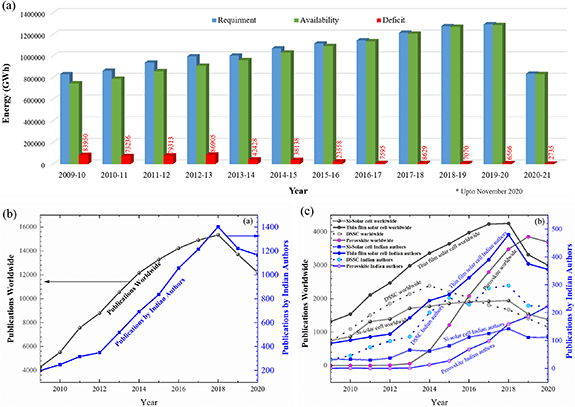
Figure 1. (a) Energy demand-supply scenario in India (data taken from [3] upto Nov. 2020); (b) annual publication trend on solar cells (data obtained from Clarivate Analytics retrieved on 10/11/2020) and (c) annual publication trend on different technologies of the solar cell (data obtained from Clarivate Analytics retrieved on 10/11/2020).
Download figure:
Standard image High-resolution imageIndia is blessed with 300 clear sunny days in a year showing vast solar energy potential [5]. The theoretically estimated solar energy incidence on the Indian peninsula is about 5 000 trillion kilowatt hours (kWh) per year [6]. Therefore, the migration from conventional energy sources to solar energy can improve energy security, mitigate climate change, and reduce carbon footprint. Enormous efforts have been put together for developing economically viable solar energy. For instance, the solar tariff has reached its all-time low below 2, which is lower than the existing thermal power in India. As of December 2019, the grid-connected Si solar modules installed in solar parks and solar rooftop installation generate 39 712 MW in India [7]. Apart from these solar module installations, a standalone solar lamp program for indoor lighting is also being used in many remote locations all across India. Traditional photovoltaic cells (1st and 2nd generation) such as amorphous silicon (a-Si: H), gallium arsenide, copper indium gallium selenide (CIGSe), and cadmium telluride (CdTe) and their solar modules are commercially available for real-life applications [8–10]. Despite the rapid progress in traditional photovoltaics, these cells still suffer from some drawbacks such as relatively high cost associated with ultra-high purity requirement for the active material (Si), scarcity of materials (indium, gallium, and telluride), the toxicity of cadmium, and low working capability of the solar panels in cloudy conditions or shaded regions [9]. These drawbacks lead to photovoltaic technologies advancement, which promises to be less expensive, thinner, more flexible, and amenable to a wide range of lighting conditions, all of which make them suitable for a host of applications beyond rooftop and solar farm panel [9]. Emerging photovoltaic cells (3rd generation) include organic solar cells, perovskite solar cells, dye-sensitized solar cells (DSSCs), and earth-abundant copper zinc tin sulfide (CZTS) thin-film solar cells (TFSCs), and others [11–13]. Research progress in all these PV technologies has grown exponentially in India as well as worldwide. Figures 1(b) and (c) show the year-wise publication trend on solar cells and related technologies. Some grass-root-level research and state-of-the-art technologies have been developed to manufacture and characterize these PV materials by the Indian research community.
This review discusses the recent solar cell developments from Si solar cell to the TFSC, DSSC, and perovskite solar, along with energy storage devices. Throughout this report, the solar cells are comprehensively assessed for the attributes of cost-effective and efficient alternative materials for energy generation and storage systems. The influence of texturing, anti-reflective coating, and surface passivation on silicon solar cells performance and progress on a-Si material developments are discussed in section 2. The fundamental understanding of each constituent layer on TFSCs performance, combinatorial approach to TFSCs, and key achievements in photo conversion efficiency (PCE) of CIGSe, CZTSe TFSCs, earth-abundant light absorbers, and their device performance evaluation are discussed in section 3. In section 4, we overviewed the progress in DSSCs extensively. The effect of different counter electrode (CE) material parameters on electrochemical catalytic activity and PCE values, transparent CEs for semi-transparent DSSCs, and large area DSSCs modules are reported in section 4. The development of Pb-based and Pb-free absorbers, electron/hole transport layer, and CEs for perovskite solar cells are reviewed in section 5. Section 6 comprehensively describes energy storage devices and bi-functional devices. Section 7 deals with the prospects and untapped potential of energy conversion and storage systems.
2. Silicon solar cells
Silicon is the widely used material for photovoltaic applications due to its properties like the favorable bandgap of 1.12 eV, allowing the light absorption up to 1100 nm wavelength; natural abundancy (Si is the second most abundant element on earth); thermal stability, and others. In 1954 Chapin et al from Bell laboratory first invented and published the report on silicon solar cells having an impressive 6% efficiency [14]. Since then, Si solar cells have undergone various research and developments for more than half a century. This makes Si-solar cells the most mature PV technology. More than 90% of the global PV market is dominated by Si-based solar cells [15]. Primarily, Si solar cells are classified into three types: monocrystalline, polycrystalline, and amorphous. Monocrystalline or single-crystalline Si (sc‐Si) cells are made from sliced silicon ingot grown from solar grade single-crystal silicon with 99.9999% purity. The circular slice from the cylindrical ingot is further chopped in octagonal or hexagonal shapes depending upon the module requirements. The highest efficiency (26.1%) was reported for sc‐Si solar cells with polycrystalline silicon on oxide passivated contacts [16]. Polycrystalline or multi-crystalline Si (mc‐Si) solar cells are made from melted silicon molded in square shapes. The production of mc‐Si solar cells is easy and economical compared with monocrystalline Si cells. However, in polycrystalline solar cells, grain boundaries act as the electron/hole trapping centers, and the photogenerated minority charge carriers can be trapped at the grain boundaries, resulting in deteriorated cell performance. The grain-boundaries inject extra defect energy levels into the band gap, producing the significant localized recombination centers, thus lowers the photogenerated minority carrier lifetime. Therefore, the randomly oriented grain boundaries act as the recombination centers responsible for minority carrier lifetime reduction and provide shunt paths for lowering solar cell performance [17–19]. The highest efficiency of 23.81% was reported for mc‐Si solar cells by Canadian Solar Inc. In a-Si solar cells, a thin layer of a-Si is deposited on the substrate. The amount of Si used in the a-Si device is significantly less, and hence they are very economical. Usually, these solar cells are less efficient, the highest reported efficiency being 14% [20], but they can be fabricated on flexible substrates and can be used for small-scale applications.
The Si solar cell design involves texturization, p–n junction formation by diffusion, surface passivation, an anti-reflection coating (ARC), metal paste deposition (fingers and bus bars), and finally, encapsulation. Over the years, various device architecture of Si solar cells have been explored, such as aluminum-back surface field [21], passivated emitter rear cell (PERC) [22], passivated emitter rear locally diffused [23], metal wrap through, emitter wrap through, heterojunction with an intrinsic thin layer. Yoshikawa et al have reported the a-Si/c‐Si heterojunction device having 26.3% efficiency [24]. These developments have been focused on improving the surface passivation and controlling the recombination. From the last decade, the research on Si solar cells are more focused on minimizing various losses like photon loss (using texturization, anti-reflective coating, back-contact cell design, back surface reflector), carrier loss (using front electrode passivation and back surface passivation), and electrical loss (by improving metallization, minority carrier diffusion length). Even though there has been extensive research and developments in Si solar cells, it is commonly perceived that the fabrication of Si solar cells requires sophisticated and large industrial equipment. To resolve this, Basu et al reported 19% efficient c‐Si solar cell having 160 m2 area with Cz p-type sc-Si wafers using small footprint laboratory tools. This study has shown the potential to fabricate high-efficiency Si solar cells using low-cost lab equipment [25].
In India, research on Si solar cells was started way back in 1974 at National Physical Laboratory. Since then, various research labs have dedicatedly worked on the development of various aspects of this technology. We have discussed significant developments in the substrate material, surface passivation, reflection minimization, and encapsulation for Si solar cells in the subsequent sections by Indian research groups.
2.1. Texturing
As-cut silicon wafers are highly reflective (having more than 35% reflection [26]); therefore, it requires surface texturing to reduce light reflectance and enhance light trapping. The wafer's front surface is textured with a random vertically aligned pyramid structure, which reduces the surface reflectance. Wet chemical etching in an alkaline solution is the most commonly used method for surface texturization [27]. Before surface texturization, the wafers are usually cleaned in the acid bath to remove the cutting slurry and etch the damaged surface. The texturing time optimization is very critical since it involves a material loss for creating the pyramidal structure. This pyramidal structure is responsible for light trapping and reduction in reflectance. Singh et al studied the optical effectiveness of anisotropic etching of (1 0 0) Cz silicon. The etching was done in the solution containing 2 vol% NaOH and 20 vol% IPA at 80 °C. The texturization pattern (pyramid size) and the reduction in reflectivity are directly related to the etching time. The uniformly distributed and regular pyramidal structure was obtained for 25 min < texturization time <45 min. The Jsc improved linearly with etching time, which gets saturated at 30 min [28]. The improved Jsc is due to reduced light reflection and enhanced electron–hole pairs generation.
The pre-texturization surface treatment helps to remove the mechanically damaged surface of Si wafers and other contaminants that might get linked during the Si ingot slicing. The conventional treatment involves NaOH or KOH solution-based treatment. This method is often responsible for bad non-uniform texturization [29]. The longer pre-treatment also causes the breakage of wafers. Gangopadhyay et al have reported modified pre-texturization surface contamination removal of (1 0 0) p-type Si wafers to address these issues. The solution containing 12% sodium hypochlorite (NaOCl) at 80 °C was used for pre-texturization treatment before the saw damage removal step. The NaOCl based pre-treatment assists in removing organic contaminations by oxidation. The significant improvements in fill-factor (from 0.53 to 0.75) and efficiency (from 9.90% to 15%) were observed for the devices fabricated with NaOCl based pre-treatment. The SEM image of the wafer without NaOCl treatment and NaOCl treatment is shown in figure 2(a). This significant fill-factor improvement was attributed to improved contact formations, which otherwise poor due to surface contaminations [30]. However, this additional pre-texturization treatment creates problems like enhanced cost, lesser yield due to wafer breakage, time consumption, etc. To solve this problem, Basu et al have developed a modified process using NaOH:NaOCl in 1:3 volume ratio solution, which does pre-texturization cleaning and saw damage removal simultaneously in one step. The SEM image of the texturized wafer with modified pre-treatment is shown in figure 2(a). The solar cell fabricated with modified pre-texturization treatment has shown efficiency of 15.11% compared with 14.75% in two-step old pre-texturization treatment [31]. Figure 2(a) shows the difference between the two-step pre-texturization treatment involving separate saw-damage removal step as reported by Gangopadhyay et al [30] (on the left side of the figure, highlighted with orange route 1) and modified one-step pre-texturization treatment reported by Basu et al [31] (on the right side of the figure, highlighted with blue route 2).

Figure 2. (a) Process flow diagram for the pre-texturization treatment of Si wafer showing the difference in two-step pre-texturization involving separate saw damage removal step (route 1). Reprinted from [30], Copyright (2007), with permission from Elsevier, and modified one-step treatment (route 2). Reprinted from [31], Copyright (2010), with permission from Elsevier. (b) Process flow diagram of 'NCPRE acid texturing' (modified steps are shown in dotted box) [33]. Reprinted from [33], Copyright (2019), with permission from Elsevier. PL imaging under open circuit condition (c) and RS distribution (d) for solar cells with different metallization configuration [35]. Reprinted from [35], Copyright (2020), with permission from Elsevier.
Download figure:
Standard image High-resolution imageSrivastava et al have reported Ag catalyzed wet chemical etching based texturing of (1 0 0) p-type Si surface. This two-step texturization process involves thin Ag film deposition using electroless plating technique in the first step and finally wet chemical etching in a solution containing H2O2:HF:DI water in 1:2:10 volume ratio. The residual Ag was removed by etching in ammonia and H2O2 solution. The reflectivity of <4% was achieved. The fabricated n+–p–p+ solar cells using this texturized surface shows >20% (from 23.9 to 28.9 mA cm2) improvement in Jsc compared to the planar Si surface-based device [32]. Sreejith et al have developed an additive-free novel texturing process of diamond-wire-sawing based mc‐Si wafer. This technique was termed the 'NCPRE acid texturing process.' The texturization process involves wet chemical etching of wafer in HF rich HF: HNO3 solution to make porous Si and subsequently dipping it in KOH solution for dissolving porous Si and creating the textured surface. The process flow diagram of the developed technique with modified steps is shown in figure 2(b). The weighted average reflectance of the textured wafers are ∼29.0% and ∼6.5% after anti-reflective coating post texturization. The fabricated solar cell has shown efficiency of 18.46% [33]. Later, the same method was adopted to fabricate large-area (156.75 × 156.75 mm2) industrial-scale solar cells. The cells fabricated with additive-free 'NCPRE acid texturing process' have shown the efficiency of 18.20%, comparable with solar cells fabricated using commercial GP solar texture additive-based texturization method having 18.24% efficiency [34].
To obtain better contacts, efficient current collection, and minimize the fill-factor loss, metallization is required. Typically screen printing of Ag is used for metallization. Although these metal grids help to reduce electrical losses, they contribute to shading (optical) losses. Behera et al studied six different metallization designs with 86 and 96 fingers with three, four, and five bus bars. The photoluminescence (PL) imaging technique was used to quantify the losses. It was reported that group A (cell with 86 fingers and three bus bars) shows the highest PL intensity and series resistance (RS) figure 2(c). In contrast, the cells with 96 fingers and five bus bars (group F) show the lowest PL intensity and RS shown in figure 2(d). The group A devices have shown the highest Jsc and Voc; on the other hand, the group F devices offer the highest FF. The best efficiency of 18.04% was reported for 86 fingers and five bus bars configuration (group C) [35].
2.2. Anti-reflective coating
To further reduce the reflection and enhance light absorption, an ARC is applied. The coating consists of a thin layer of dielectric material directly coated over the protective glass or directly on the cell. The thickness of the ARC material also decides the solar cell color [36]. Prasad et al were the first to report anti-reflective coating by anodic dissolution and redepositing porous Si. Photostimulated chemical etching using HF-based electrolyte was used instead of conventional electrochemical anodization; no external electrical field was applied. The ellipsometric measurements have shown the reflective index of the order of 1.95 ± 0.05 for 74 ± 2 nm thickness. This novel anti-reflective coating technique had reduced the optical losses from 37% to 8% and improved the Jsc by 25% [37]. After this work, porous Si-based anti-reflective coating was widely used in solar cells; the detailed description and advantages of porous Si-based anti-reflective coating are discussed in [38, 39].
Kishore R, Singh S, and Das B have used silicon nitride (Si3N4) and titanium oxide (TiO) deposited using plasma-enhanced chemical vapor deposition (PECVD) and screen-printing, respectively, for ARC purposes. 85–90 nm Si3N4 has shown the maximum enhancement of 23.2% in the Jsc for textured solar cells; this enhancement is attributed to the passivation and anti-reflective properties of the Si3N4. On the other hand, TiO based ARC on polished Si wafer enhances the Jsc up to 27.7% [40]. Srivastava et al, in their work, prepared vertically aligned silicon nanowires using wet chemical etching of p-type silicon substrate for antireflection purposes. The etching was done using a solution containing HF and AgNO3. The reflectivity can be tuned by the increasing etching time. This process helps in minimizing the reflection losses to ∼2%. The fabricated solar cells have shown up to 20% improvement in Jsc [41]. Aluminum doped zinc oxide (AZO) thin film synthesized using sol-gel was used as ARC on n+–p–p+ type sc-Si solar cells by Verma et al AZO films having excellent transmittance (∼90%) have shown a significant reduction in reflectance. However, due to improper metallization and contact-making, the fabricated solar cell with 58–62 nm thick AZO has shown a poor Isc of 237 mA [42]. Prathap et al demonstrated In2O3 nanocone-based ARC on the Si surface. The anti-reflective nanostructure was deposited using thermal evaporation of carbothermal reduced In2O3 powders and annealed at 300 °C–450 °C. The deposited films significantly reduce the reflectance up to 3% with the high optical transmission (∼90%) [43]. Amorphous barium titanate (a-BTO) deposited using RF sputtering was used as ARC by Sharma et al [44]. The 70 nm thick a-BTO coating had 85% visible region transmittance and has shown 100% reflectance reduction on polished Si substrate at 550 nm and 85% reduction for textured Si at 400 nm. The a-BTO ARC-based sc-Si solar cells have improved efficiency by 7.5% [44]. Vertically aligned Si-nanocones arrays having superior anti-reflectivity properties (∼2.0% reflectance) were fabricated on p-type (1 0 0) silicon using inductively coupled plasma–reactive ion etching (ICP-RIE) technique by Katiyar et al [45]. In their work, they have fabricated n-CdS/pSi-based heterojunction solar cells using planar Si, chemically etched Si, and ICP-RIE based Si having the efficiency of 0.15%, 0.66%, and 2.96%, respectively. The significantly improved efficiency in the case of ICP-RIE based Si nanostructure is due to its conical structure and enhanced anti-reflectivity [45]. Comparison of three different transition metal oxide (TMO) (zinc oxide, magnesium oxide, and aluminum oxide) based ARC deposited by RF sputtering on p-type Si wafer was reported by Sagar and Rao [46]. The solar cell with the 80–95 nm thick ARC has shown significant Jsc enhancement, which was highest in the MgO coated device (26.45 mAcm−2 compared to the reference cell having 20.75 mAcm−2) [46].
2.3. Surface passivation
The passivating layer is introduced to minimize surface recombination losses in the device. This passivation layer saturates the dangling bonds on the surface, reducing the surface state density, which helps minimize recombination losses and is vital for high-efficiency solar cells [47]. Several materials like Al2O3, SiO2, and Si3N4 with various deposition techniques such as thermal oxidation, PECVD, atomic layer deposition (ALD), and atmospheric pressure chemical vapor deposition have been explored for surface passivation. SiO2 is most favorable for the passivation, and it has shown superior passivation for both n and p-type Si wafers [48]. High temperature (∼1000 °C) oxidation of silicon surface is the most commonly used technique for passivation; however, this method has several drawbacks. Exposure to high temperature degrades the bulk carrier lifetime also affects the metal contacts; above all, it adds to the solar cell production cost.
Considering this, Jana et al have used photo-CVD and RF-PECVD techniques for low-temperature deposition of silicon oxide and Si3N4-based passivation layer, respectively. Photo-CVD-based silicon oxide was done using silane, CO2, and hydrogen gases at 250 °C, whereas Si3N4 was deposited using silane, ammonia, and hydrogen gases [49]. An 80 nm passivating layer of silicon oxide improves the Jsc by 5.8%, and the Si3N4 passivating layer of the same thickness improves the Jsc by 10.2%. The improvement in efficiency after the passivation was 6.7% and 11.16% for silicon oxide and Si3N4 [49]. Yadav et al have used a chemical oxide growth process using hot NaOCl solution to grow a thin layer of SiOx on the 5 inch p-type Si wafers, which were then capped with SiNx : H layer using PVCVD, thus forming SiNx :H/SiOx stack in the two-step method. This modified technique was termed 'NCPRE-oxide passivation' [50]. The NCPRE-oxide passivation (SiNx : H/SiOx ) was elucidated by lower emitter saturation current density (140 fA cm−2) than conventional SiNx :H based deposition (167 fA cm−2); this leads to improvement in Voc and efficiency [50]. Expanding this work, the same group have compared NCPRE-oxide passivation method with different SiOx layer deposition technique. Thermal oxidation, nitric acid-assisted oxidation, PECVD based oxidation, UV–ozone-assisted oxidation, RCA-2 solution (hot HCl/H2O2/H2O) based oxidation, and piranha solution (H2SO4:H2O2 in 4:1 ratio) based oxidation method were compared with the NCPRE-oxide method. After the SiOx layer, SiNx :H layer was deposited using PVCVD. The quality of passivation can be visualized from the PL images of Si wafers after passivation (figure 3(I)). All the wafers have shown uniformity except for nitric acid-assisted oxidation-based wafers (figure 3(I_d)). Further, the PL image of the solar cells in open circuit condition fabricated with these wafers shows the highest and lowest PL count in the case of thermal oxidation and nitric acid assisted oxidation, respectively, in the cased of SiNx :H/SiOx stack passivated devices (figure 3(II)). Solar cell with single SiNy:H layer shows the minimum (darkest) PL intensity (figure 3(II_h), as anticipated. Higher PL intensity symbolizes better passivation and thus improvement in the Voc. In this work, they have shown that although the thermal oxidation-based SiOx layer has shown best passivation, it is not suitable for bulk manufacturing due to its high-temperature requirement. Thus the developed 'NCPRE-oxide passivation' can be the appropriate alternative, as it shows comparable results (Voc: 630.5 mV and efficiency: 18.4%) with the best performing thermal oxidation based SiOx layer (Voc: 633.9 mV and efficiency: 18.6%) [51].

Figure 3. PL images of (i) wafers and (ii) solar cells in open circuit conditions prepared with (a) thermal oxidation, (b) NCPRE oxide, (c) RCA-2, (d) nitric acid assisted, (e) piranha, (f) ozone assisted, (g) PECVD based SiOx for SiNx :H/SiOx stack and (h) SiNy :H without SiOx layer [51]. Reprinted from [51], Copyright (2019), with permission from Elsevier. Encapsulation of solar cell: (iii) visual image (iv) fluorescence image and (v) transmittance spectra of double-layer TPO and EVA laminates [65]. Reprinted from [65], Copyright (2019), with permission from Elsevier.
Download figure:
Standard image High-resolution image2.4. Amorphous silicon material developments
Saha et al have prepared phosphorus-doped n-type microcrystalline hydrogenated silicon (Si:H) films using RF enhanced CVD system and studied its electrical and optical properties [52]. The prepared Si:H has a conductivity of 100 S cm−1. Later the same group has reported a series of research papers on the optimization and utilization of Si:H in solar cells. N-type Si:H was used in p-i-n/p-i-n double junction solar cell. The FF was improved from 0.628 to 0.731 and Voc from 1.69 to 1.80 V by replacing the amorphous layer with the microcrystalline Si:H. The overall efficiency was improved from 7.75% to 9.74% [53]. In another work, the dependences of Si:H film thickness on the electro-optical properties were discussed. It was observed that thin layers remained amorphous, and the minimum 30 nm thickness was required for the nucleation of crystallites. The 75 nm thick film, deposited at 120 mW cm−2, has shown prominent microcrystalline growth [54]. A similar method was adapted by Sarker et al for the deposition of n-type microcrystalline hydrogenated silicon oxide (Si:OH). The prepared Si:OH has a higher bandgap of 2.17 eV than deposited microcrystalline Si:H has a 2.07 eV bandgap. The higher bandgap of Si:OH was due to the amorphous Si-O phase in Si:OH [55]. Later, Funde et al used a similar deposition technique and studied the influence of hydrogen dilution on Si: H's electro-optical properties. For the optimized conditions, highly crystalline and wide bandgap (2.25 eV) n-type Si:H was obtained with only 6.5 at% hydrogens [56].
2.5. Encapsulation
Encapsulate material is a vital component of the solar cell, as it protects the solar cell and ensures long-term performance. The prime requirement of encapsulating material is optical transparency, excellent adhesion, and moisture resistivity. It also provides mechanical support, physical insulation, and protection. Ethylene-vinyl acetate (EVA) is the most commonly used encapsulant, which has been used in Si solar cells since the 1980s. Apart from EVA, thermoplastic polyurethane [57], polyvinyl butyral [58], silicone [59] have also been explored, but either is too expensive or unstable. A good encapsulate should have high thermal stability and low glass transition temperature (Tg). When the hot-spot is created on the solar module due to defects, depending on the defect area, the local cell temperature reaches as high as 294 °C [60]. This is the reason for the high melting point requirement. The glass transition from a rigid glassy state to a viscous state with an increase in temperature. Below Tg, the material is hard and brittle; above Tg, it is flexible. Therefore lower Tg provides a large operation window for solar cells [61]. The Tg for EVA encapsulates −38.66 °C, and it is thermally stable up to 285.13 °C [62]. Even though EVA has dominated the solar cell industry, it undergoes yellow-to-brown discoloration due to photothermal and photochemical degradation. EVA degradation (browning) was first observed in the late 1980s at Carrisa Plains PV power plant in US, where the annual output was reduced by >45% within 5 years (1986–90) [63]. Since then, researches worldwide have tried to stabilize the EVA and explore various other alternative encapsulates.
Thermoplastic polyolefin (TPO) based encapsulant was explored by Adothu et al [64, 65]. TPO is a non-cross linking polymer having a high melting point compared with EVA. With similar transmittance, it is more thermally stable than EVA [64, 66]. In EVA, irreversible degradation can be observed at 260 °C, whereas TPO is significantly durable for temperatures below 400 °C. High-temperature stability is essential for preventing encapsulant degradation during hot-spot conditions. TPO provides higher peel adhesion strength with lesser lamination time [64]. The long-term UV-365 exposure test showed discoloration in EVA encapsulant after 50 d, whereas no discoloration was observed in TPO encapsulant, as shown in figure 3 (iii and iv). These discolorations can only be detected by fluorescence imaging. In the double-layer laminates configuration after 50 d of UV-365 exposure, for EVA-based laminate, the transmittance is decreased from 93% to 88% in the range of 380–700 nm. In contrast, TPO-based laminate remains unchanged (figure 3(v)) [65]. These studies have shown that TPO encapsulates have better thermal stability, optical properties, and adhesion; hence, they can replace EVA-based encapsulates, which will ensure the long-term performance stability of solar cells. polymethyl methacrylate (PMMA) based encapsulation for mc-Si solar cells was reported by Mohan et al They have also done EVA, polyethylene terephthalate pouch based lamination [67]. This technique can be suitable for lab-scale fabrication but cannot be implemented for large-area industrial solar cells and have reliability issues.
To summarize, in India, extensive research is going on each component and aspect of Si solar cells. However, India still imports a considerable amount of solar cells and modules. In the first nine months of 2019, India has imported USD 1.6 billion worth of solar cells and modules [68]. To minimize this, India needs rapid industrialization of indigenously developed technological advancements. Being the most mature solar photovoltaic technology, Si solar cells are the most commercialized technology as well. Of the 707.5 GW installation of solar photovoltaic worldwide [69], Si solar cell technology accounts for ∼90% of the market share [70]. This is majorly dominated by c‐Si solar cells, accounting for more than 65% of global annual production [15, 71]. With the ever-growing market, the Si photovoltaic manufacturing companies heavily invested in automation for higher throughput. The continuous efficiency improvement and improvement in manufacturing processes resulted in increasing module power. Despite the maturity of this technology, various aspects like passivating contacts (PERC and tunnel oxide passivated contact (TOPCon), reducing metal coverage (fingers and bus-bar width), and improved encapsulation are being continuously upgraded. The solar photovoltaic industry is now focusing on bifacial modules [72], floating PV solar tiles, or solar slates. Additionally, Silicon in tandem with another III–V-based or emerging perovskite top cell provides the opportunity to cross Shockley–Queisser single-junction theoretical limit. Nevertheless, overall the Si solar cell technology has some demerits, such as vacuum-based processing, and they are relatively expensive. Its fragile nature makes them prone to physical damage during transportation and installation. To overcome these issues, several other PV technologies are being explored.
3. Thin-film solar cells
The TFSCs are the second generation of solar cells. These are fabricated by depositing one or multiple thin films on a suitable substrate. The films are way thinner than conventional c-Si wafers making TFSC pannels lighter. The major advantage is that TFSCs can be fabricated on flexible substrates. Traditional TFSCs such as Cu2(In, Ga)Se2 (CIGSe), and CdTe have reached over 20% device efficiency [8]. However, the scalability of such devices limited by elemental scarcity (In, Ga) and toxicity (Cd) issues. It is essential to develop earth-abundant absorber materials and high throughput processes for TFSCs to reduce the overall cost of the device to meet the global energy demands [73]. Typically, TFSCs consist of (a) back contact (Mo), (b) a light-absorbing layer (p-type, CIGSe), (c) a contact layer (n-type, also known as window or buffer layer), (d) a transparent conductive layer (front electrode), (e) a metal layer (back electrode), and (f) an anti-reflective coating [74]. Each of these layers has a role in the performance of TFSC. For example, the buffer layer (usually cadmium sulfide (CdS) film) plays a vital role in p–n heterojunction formation, and hence in the transport of photogenerated electric charge carriers to the external circuit. A detailed discussion of the role of CdS and i-ZnO on CIGS-based TFSCs is provided in section 3.5. The important aspects of components in TFSCs are discussed below based on previously reported literature.
3.1. Back contact
The back contact is primarily utilized to carry various functions such as form an ohmic contact, reduce recombination at back contact and act as a back reflector for incident photons in the case of a thin absorber layer (<1 µm) [75]. The basic requirements of a back contact material for (CIGS and CZTS) thin solar cells maintain certain inertness to the corrosive atmosphere during film deposition and low recombination rates for minority carriers along with forming ohmic contact [75]. In this sense, molybdenum (Mo) is one of the popular choices fulfilling the desired quality of back contact materials [75]. Mo layer offers high stability to a processing temperature (up to 600 °C), good adherence to the substrate (which is usually glass), does not react with or diffuse into the CIGS since it forms a low-resistive contact with CIGS [75].
3.2. Absorber layer
The TFSCs constitutes absorber layer for absorbing the incident light and generate the electron–hole pair [74, 76]. The selection criteria for the light absorbing materials for TFSCs includes: (a) suitable optical band gap of 1.0 eV < Eg < 1.5 eV, (b) high absorption coefficient >104 cm−1, (c) long lifetime, drift length/diffusion length of minority carriers, (d) low surface recombination velocity, (e) eco-friendly and reproducible deposition technique for light absorber on inexpensive substrates, (f) energy balance/energy payback time, (g) production and operation of device with full of safety [74, 76]. For instance, Cu2InSe2(CISe), Cu2InGaSe2(CIGSe), CdTe, and Cu2ZnSnS4 (CZTS) light absorbers have been utilized for TFSCs [10, 73, 74, 77, 78].
Cu(In, Ga)Se2 (CIGSe) thin films have been prepared via different solution processes such as spray casting and ink-jet printing techniques [79–81]. The thickness, morphology, chemical composition ratio, sodium, sintering techniques, and selenization time of the absorber layer impact CIGSe TFSCs (Al:ZnO/i:ZnO/CdS/CIGS/Mo/SLG) performance were investigated in the literature [79–81]. The efficiency increased from 0.34% to 3.4%, increasing the selenization time from 5 to 25 min. The enhancement in PCE is attributed to the large grain size and carrier concentration control [81]. The higher PCE (3.2 ± 0.2%) was reported for NaF doped CIGSe based TFSCs compared to the undoped CIGSe device (1.5%). The thickness, surface morphology, and NaF doping of CIGSe absorber significantly improved TFSCs performance [81]. For instance, the PCE values of TFSCs were increased from 1.8% to 6.7%, analogous to an increase from 0.75 to 2.5 µm in the thickness of CIGSe [81]. The steady increment in Voc and Jsc contributes to improved device performance [81]. The high absorption coefficient (∼105 cm−1), better packing density, and thicker CIGSe films (2.5 μm) are sufficient to absorb incident sunlight, thus ascribes to the improvement in CIGS TFSCs [81]. The PCE value of thermally evaporated CIGSe absorber for CIGSe based TFSCs was estimated to be 13.8% [82]. The performance of CIGSe solar cells is lower as compared to worldwide reported efficiency (>22%). Further studies are required to optimize CIGSe film quality, chemical compositional ratio, and interfacial recombination to achieve higher performance of CIGSe TFSCs.
Earth-abundant Cu2ZnSnX4 based (CZTS/Se, X = S, Se) light absorbers have been prepared via wet chemical (nanoparticles based films), direct solution coating, sputtering, and pulsed laser deposition technique [83–91]. The Cu2ZnSn(Sx Sex -4) (CZTSSe) nanoparticles were synthesized via the thermolysis process, and the film prepared from the synthesized nanoparticles was utilized as a light absorber for TFSCs [88]. The nanoparticles size, S/Se composition ratio affected the performance of CZTSSe based TFSCs [88, 90]. The PCE value is increased from 3.6% to 4.8% with an increase in the size of nanoparticles; thus, changes in the PCE value of CZTS based TFSCs are speculated due to the variation of the thin film's microstructure [88]. The PCE values of CZTS, CZTSe, CZTSSe based TFSCs were determined to be 4.5 ± 0.12%, 5.1 ± 0.10% and 7.4 ± 0.12% respectively [90]. The changes in the device performance might be attributed to the variation of the optical band gap, RS, shunt resistance (RSH), and the microstructure of the thin films [90]. The successive ionic-layer adsorption and reaction (SILAR) processed Cu2ZnSn(S,Se)4 (CZTSSe) light absorbers were reported for TFSCs [92]. The highest PCEs of devices based on CZTS and CZTSSe absorber layers were 1.96% and 3.74%, respectively [92]. The difference in the PCE value of CZTS and CZTSSe based TFSCs was mainly due to the microstructural changes in thin films [92]. The PCE can be further enhanced with optimal preparation parameters and post-annealing conditions for the CZTSSe absorber layers [92]. Cu2ZnSnS4 thin films prepared by the replacement reaction process were used as a light absorber for TFSCs [83]. The fabricated CZTS based TFSCs (graphite/CZTS/CdS/ZnO/ITO/SLG) has exhibited the PCE of 6.17% [83]. The RS and RSH of TFSCs are 5.8 and 680 Ω cm−2, respectively. The high RS value results in low JSC, thus lowering the PCE of TFSCs [83]. The annealing of the device at elevated temperatures and using ITO substrate with lower sheet resistance lowers the overall RS. The sol-gel spin-coated CZTS films based TFSCs were reported with PCEs of 3.01% in the literature [83]. The inferior PCE of TFSCs is attributed to the low FF and copper-rich chemical composition of CZTS films. The low FF is affected by high sheet resistance and low RSH values of 333.33 and 47.91 Ω cm2, respectively [83]. The impact of Zn/Sn ratio, secondary phase (Cu2-x S), thickness, and annealing temperature on sputtered CZTS based TFSCs performance were investigated in the literature [87, 91]. The presence of Cu-S based secondary phases in CZTS films provides shunting paths to the current flow, thus critically affecting the device performance [91]. For instance, the PCE value was increased from 1.8% to 6.11% while reducing the Zn/Sn ratio from 2.55 to 1.20 [91]. The variation of device performance is due to changes in RSH. Controlling the Zn/Sn ratio resulted in an effective and virtuous solution to avoid the detrimental secondary phases like Cu2-x S [91]. The fabricated TFSCs (Ag/ITO/i-ZnO/CdS/CZTS/Mo/SLG) with optimum composition (Zn/Sn = 1.10) of co-sputtered CZTS showed the highest PCE of 6.11% without any ARC [91]. Based on reported literature [93–96], the inferior performance of CZTS (or Se) based TFSCs is mainly due to deficiency of Voc and lower fill factor (FF). The FF can be improved by optimizing device processing conditions, which control the RSH and RS values of the devices [93–96]. The deficiency of Voc of CZTS (or Se) devices can be possibly due to the presence of deep defects, compositional inhomogeneities, bandgap fluctuations introduced by cationic disorder, low carriers lifetime, secondary phases, and interfacial recombination of the buffer/absorber or back electrode/absorber [93, 94]. Further research is underway to better understand and improve the interfacial recombination at the back electrode, absorber /buffer layer, passivation of deep defects, controlling the secondary phases, and other plausible reasons to enhance CZTSSe TFSCs performance [73, 93, 94].
3.3. Buffer layer
The buffer layer (CdS contact) manifests with the formation of a heterojunction with a light-absorbing layer (CZTS, CIGSe, CISe). CdS is expected to be extensively transparent to the incident radiation on the absorbing layer, facilitating photogenerated carriers effective transport to the outer circuit [93, 97]. The CdS layer functionality is not limited to the heterojunction partner. It is vitally utilized within band alignment, lattice matching, low interface recombination, and formation of a buried heterojunction via Cd doping CZTS and CIGS solar cells [93, 97, 98]. The thickness of the CdS buffer layer is crucial as it may lead to the shunting between the absorber and the electrode (too thin contact) or the high RS of the PV devices (too thick contact), and hence governs the trade-off between the photon absorption and carrier collection [93, 97, 98]. The device performance is also affected by CdS thickness; the optimum thickness of the CdS layer is 40 ± 10 nm, beyond which the device efficiency starts decreasing due to the increased absorption in the CdS [82, 97]. Apart from the CdS, several alternative buffers such as ZnS, In2S3, ZnSe, SnO2, ZnO materials, and Zn(O, S), ZnO/ZnS, (Zn, Mg)O, TiO2, (Cd, Zn)S, In(OH, S), and others.) have been reported for CIGSe, CISe, CZTSe solar cells in the literature [73, 77, 82, 89, 93, 98–103].
3.4. Intrinsic ZnO/AZO layers
The intrinsic ZnO layer, is highly resistive and prevents the current leakage in the buffer layers, CIGS thin films, and the AZO [104]. The thickness of i-ZnO has a vital role in device performance. The optimal thickness of the i-ZnO layer with device performance has been reported around 50–70 [104]. AZO has good electrical conductivity and high transparency in the visible spectrum. The primary function of the AZO layer is to transmit most of the incident light into the absorber layer and conduct the current to the outer circuit [97]. Transparent conductive oxide (TCO) is used exclusively as the top contact metal grids [97]. Ni-Al is usually deposited on top of the TCO to reduce the RS. At the same time, Ni prevents the formation of a resistive Al2O3 barrier, and the thickness of Ni, Al layers have been optimized to 50 nm, 1 µm thick, respectively [97].
3.5. Impact of CdS and I-ZnO layers on CIGSe thin-film solar cells performance
Krishnaiah et al experimentally studied the effect of CdS and I-ZnO layers on CIGSe TFSCs performance. The schematic diagram and experimental results of TFSCs are shown in figure 4. The performance parameters of TFSCs without CdS layer such as open-circuit voltage (Voc), short circuit current density (Jsc), FF, and efficiency (η) (Glass (SLG)/Mo/CIGSe/i-ZnO-AZO/Al-Ni, figures 4(a) and (b)) were found to be 350 mV, 25 mA cm−2, 49%, and 4% respectively. The inferior device performance can be accounted to one of many reasons such as PN junction damage, direct sputtering of i-ZnO affecting the surface of CIGSe layer, interfacial recombination leading to lower RSH (540 Ω cm−2), and thus resulting in more shunt paths between the TCO/Mo [82, 93, 97, 98, 104]. The Voc, Jsc, FF, and η of the device without an i-ZnO layer in TFSCs (Glass (SLG)/Mo/CIGSe/CdS/AZO/Al-Ni) (figures 4(c) and (d)) parameters were found to be 580 mV, 29 mA cm−2, 58%, and 9% respectively. The device performance improvement was due to considerable RSH (847 Ω cm−2), indicating the minimization of shunt paths between the TCO/Mo with the CdS-AZO configuration. Further enhancement in the TFSCs parameters was obtained for complete device configuration (glass (SLG)/Mo/CIGSe/CdS/i-ZnO-AZO/Al-Ni) (figures 4(e) and (f)). The device performance parameters were determined to be Voc: 610 mV, Jsc: 31 mA cm−2, FF: 57%, and η: 10.8%. Overall, our experimental observation indicates that a CdS and I-ZnO layer on CIGSe TFSCs betters the overall performance.

Figure 4. Effect of CdS and I-ZnO layer on CIGSe TFSCs: under the illumination of 100 mW cm−2: schematic and corresponding I–V curves for the device structure (a) without CdS, (b) without i-ZnO, and (c) complete device structure, respectively.
Download figure:
Standard image High-resolution image3.6. Combinatorial approach for thin-film solar cells
The high-throughput combinatorial experimental method is the rapid and efficient method for discovering and optimizing new materials for many applications [82, 105–109]. This approach can produce a library of samples that contains a variation of a material parameter of interest, such as chemical composition, substrate temperature, layer thickness, as a function of position on the substrate [82, 105–109]. The following spatially resolved measurements of these parameters and the resulting sample properties rapidly evolve the optimization of new and existing materials. The combinatorial process has been used in TFSCs to accelerate the rate of discovery and optimization of earth-abundant non-toxic materials for absorbers, window/buffer layer, and transparent conductive electrodes [82, 105–107]. For example, Krishnaiah et al studied the combinatorial approach in buffer/contact/window layers and their integration into TFSCs to accelerate the rate of research [82]. The combinatorial chemical bath deposition of buffer/contact/window layer as CdS for TFSCs (CIGSe, CZTSe)[82]. The combinatorial synthesis of the CdS buffer layer for TFSCs is possible by dip coating. Instead of studying the effect of the buffer layer thickness on the solar cell performance in a serial, sample-by-sample manner, the combinatorial dip-coating method allows parallel screening of many thicknesses of the buffer layers prepared by chemical bath deposition [82]. The experimental set for combinatorial dip-coated CdS buffer layers and their integration in TFSCs are shown in figures 5(a) and (b). The continuous gradient in the thickness of (CdS) buffer layers for TFSCs (CIGSe and CZTSe) has been achieved via the combinatorial dip-coating process (figure 5(c)). The color difference on the absorbers' surface indicates the gradient in the thickness of the CdS buffer layer (figure 5(c)). The gradient effect of the thickness of the CdS buffer layer on TFSCs parameters is displayed in figures 5(d)–(g).

Figure 5. (a) combinatorial dip-coating process of buffer layer for light absorbers for thin films solar cells, (b) the gradient in the thickness of the CdS buffer layer via the combinatorial dip-coating process and their integration in TFSCs, (c) color difference in absorbers indicates the gradient in the thickness of the CdS buffer layer and (d)–(g) effect of thickness of CdS deposition time on TFSCs performance [82]. Reprinted with permission from [82]. Copyright (2016) American Chemical Society.
Download figure:
Standard image High-resolution imageThe dipping time significantly affects the thickness of layer deposition of CdS. The shorter dipping time leads to the shunting between the absorber and the electrode (too thin contact). In comparison, the longer dipping coating time is accredited to the high RS of the PV devices arising from the thicker CdS layer. Hence, it may influence the trade-off between photon absorption and carrier collection [82, 110]. The maximum PCE values of CIGSe and CZTSe based TFSCs were determined to 12.9% and 4.3% for 15 min dip coating time, respectively. The trends in the PCE and the spectral response of the TFSCs as a function of the thickness of the CdS buffer were explained from the perspective of microscopic and morphological characterization of CdS thin films optical and morphological perspective of the CdS thin films [82, 110]. The PCE values of CIGSe and CZTSe based TFSCs fabricated using conventional chemical bath deposition were 13.8% and 4.8%, respectively [82, 110]. The maximum PV efficiency achieved for the combinatorial dip-coating CBD was similar to that for the PV devices processed using conventional CBD. This study sums up that the combinatorial dip-coating accelerates the optimization of PV device performance of CdS and other candidate contact layers for a wide range of emerging absorbers.
3.7. Earth-abundant absorbers for thin-film solar cells
Recently, several materials such as binary sulfides (CuS, SnS, Sb2S3), ternary chalcogenides (CuSbS2, Cu2SnS3), quaternary chalcogenides Cu2(MII)SnS4 (MII = Mn, Fe, Co, Ni), and oxides (CuO, Cu2O, Fe2O3, Co3O4, and BiFeO3 (BFO)) have been investigated as an earth-abundant light absorber for TFSCs and demonstrated on a laboratory scale [111–125]. The experimentally obtained optical properties of earth-abundant absorbers were reported to be the direct optical bandgap in the range of 1.0–1.7 eV and high absorption coefficient (∼105–104cm−1); these are suitable for light absorption in the visible region [111–125]. The resistivity, mobility of solution-processed Cu2CoSnS4 (CCTS) and Cu2CdSnS4 (CCdTS) films were found to be 2 Ω cm–3.2 × 10⁻³Ω cm, 11.5–36 cm2 Vs−1 and 0.98 Ω cm–7 × 10⁻²Ω cm, 21.35 cm2 Vs−1 [110, 113, 126], respectively. Similarly, the resistivity, mobility of Cu2FeSnS4 (CFTS) and Cu2MnSnS4 (CMTS) films prepared by using drop casting technique were found to be 14 Ω cm–6 × 10⁻²Ω cm, 0.09–7 cm2 Vs−1 and 20 Ω cm, 0.11 cm2 Vs−1, respectively [90, 110, 126]. According to the reported literature, the chemical composition ratio, surface morphology, thickness, secondary phase, grain size, annealing temperature/time, annealing atmosphere, defects like vacancies (VCu, VSn, VS), antisites (CuNi, NiCu, CuSn, SnCu, NiSn, SnNi), interstitial (Cui and Nii) and defect complexes impact on optical and electrical properties of chalcogenides [110, 114, 126]. For instance, the effect of dip cycles on chemical composition ratios (Ni/Sn, Cu/(Cu + Ni)) and their interpretation on optical and electrical properties of direct solution dip-coated Cu2NiSnS4 (CNTS) films were examined [114]. The optical band gap, electrical resistivity and mobility of prepared CNTS films were found to be 1.50–1.29 eV, 0.97 ± 0.04 Ωcm–0.14 Ωcm, 1.03 ± 0.07 cm2 Vs−1–11.00 ± 0.07 cm2 Vs−1 [114]. The prepared light absorbers were utilized for both photo-electrochemical TFSCs and TFSCs. For example, Ananthoju et al synthesize Cu2FeSnS4 (CFTS), Cu2MnSnS4 (CMTS) nanoparticles and utilized nanoparticles-based films as light absorbers [90]. The fabricated CFTS and CMTS based TFSCs have displayed PCE values of 0.4 ± 0.04%, and 0.7 ± 0.02%, respectively [90]. The inferior TFSCs performance was due to the low RSH, high RS, charge carrier recombination at the interface of Mo/absorber layer, and the poor carrier collection at the electrodes [90]. Ghosh et al reported the solution-processed CCTS, CFTS, and CNTS films for photo-electrochemical TFSCs (ITO/ZnO-NR's/ZnS/Cu2XSnS4/Au) [121]. The fabricated devices depicted the PCE values of 2.73%, 3.23%, and 2.71% for CFTS, CCTS, and CNTS photoactive electrodes in 0.1 M NaOH electrolyte solution, respectively [121].
Suryawanshi M reported the aqueous precursor solution processing of earth-abundant Cu2SnS3 (CTS) absorbers for TFSCs [122]. The CTS-based TFSCs (Mo/CTS/CdS/i-ZnO/n-ZnO/Al) have shown reproducible PCE of 1.80% and exhibited good stability over three months in the air without encapsulation at RT [122]. The CTS device performance was slightly degraded under accelerated aging for 100 h at 80 °C under normal laboratory conditions [122]. The poor performance is attributed to the large RS value caused by the formation of the MoS2 layer at the CTS/Mo interface and high carrier recombination in the CTS absorber. It is also ascribed to reflection losses at the front contacts and unwanted absorption in the window layer [122]. Tiwari et al fabricated CTS light absorber via direct-coated from a single metal-organic precursor solution [123]. The TFSCs (graphite/CTS/ZnO/ITO/SLG) made with CTS absorbers displayed PCE value of 2.10% [123]. The high RS (80 Ω) may be possible for the low short circuit current and low FF [123]. Chatterjee et al fabricated the Cu2FeSnS4 (CFTS) heterojunction-based solar cells (ITO/Cu @NiO/CFTS/X/ZnO/Al) with different n-type materials (X = CdS, Bi2S3, and Ag2S) to investigate the role of electron selective materials on device performance [127]. The PCE of the fabricated devices was demonstrated to be 2.95%, 1.37%, and 0.77% for Bi2S3, CdS, and Ag2S, respectively [127]. The difference in energy offset (conduction band edge offset) at the heterojunction interface is anticipated to be the reason for the variation in the device's performance [127]. Maiti et al addressed sulfur-vacancy passivation in solution-processed Sb2S3 based heterojunction solar cells [118]. The passivation of sulfur vacancies in Sb2S3 films was obtained by controlling precursor stoichiometry (S/Sb ratio) during the film formation [118]. The sulfur deficient composition led to the formation of donor-like sulfur vacancies; a sulfur-rich stoichiometry passivated such vacancies, followed by creating sulfur antisite defects in chalcogenide [118]. The chemical composition ratio (S/Sb) affected the surface morphology and the optical band gap of Sb2S3 films [118]. The heterojunction solar cells (ITO/Cu @NiO/ Sb2S3/ PCBM/Al) fabricated with a slightly sulfur-rich composition (S/Sb ratio of 1.2) based on Sb2S3 films has shown a better PCE of 3.02% along with high Voc = 0.8 V as compared with other chemical compositional ratios [118]. The higher PCE might be due to lower charge transfer resistance (RP or layer resistance) and interfacial resistance (RS) [118]. Paul et al reported the SILAR processing of p-CuS-n-Ag2S based heterojunction solar cells [119]. The effectiveness of dopants, Sn2+, Al3+ as heterovalent-dopants on the conduction band-edge of Ag2S and their interpretation on heterojunction solar cells performance was investigated [119]. The device made with 5% Sn doped Ag2S has displayed the highest PCE of 2.85% [119]. The low bandgap metal oxides (MOs) have been considered in terms of stability and processability [124, 125, 128, 129]. Several materials such as CuO, Cu2O, Fe2O3, Co3O4, and BFO based on a heterojunction or Schottky oxide-based solar cells configuration have been studied [124, 125, 128, 129]. For instance, the solution-processed bismuth ferrite BFO light absorbers have been used in oxide solar cells [125]. The BFO/ZnO heterojunction based solar cell (graphite/BFO/ZnO/ITO/SLG), BFO made by solution processing, delivered a PCE of 3.98% [125]. The temperature-dependent BFO based solar cells were performed in the range from 140 K to 320 K. The efficiency increases with an increase in temperature, and the maximum PCE value of 4.88% was seen at 244 K, followed by a sharp decrease at further lowering of temperatures due to the strong increase in Rs [125]. The Voc linearly increases while an exponential increase in Rs displays a decrease in temperature [125]. All other oxide-based solar cells demonstrated a PCE of <1%, and the optimization of each layer in the device is expected to improve the oxide TFSCs performance [124, 128, 129].
Despite being versatile material group I–III–VI, chalcopyrite semiconductors have not achieved the required success commercially. It has captured less than 5% of the global photovoltaic market [130]. The commercialization of this technology majorly suffers due to problems associated with efficient and economic scale-up production. Being one of the most stable solar cell technology with very low degradation rate CIGS has the potential for widespread commercialization. However, this will require improved deposition methods.
4. Dye-sensitized solar cells (DSSCs)
DSSCs are third-generation solar cells fabricated from inexpensive materials with low-cost processes. O'Regan and Grätzel first reported this technology in 1991 [131]. The significant advantage of the DSSC is that it delivers desirable power output (65%–300%) on cloudy days as compared to silicon and TFSCs [8, 9, 132]. Many companies (Aisin Seiki CO. Ltd, Taiyo Yuden Co. Ltd, and Dyesol Ltd Etc) have demonstrated that DSSCs show 10% higher performance on a hot sunny day, 20% higher performance on a cloudy day compared to sc‐Si modules [9]. These studies highlight the unique features of DSSCs and their ability to work in low light conditions to overcome conventional PV technology limitations. Globally, 36 companies are working on DSSCs/modules. They have come up with several commercial applications such as liquid crystal displays, mobile phones, keyboards, solar-powered iBeacon, mouses, MP3 players, portable time clocks, mobile charger, surveillance cameras, electronic bracelets, medical devices, colorful and transparent DSSCs for building-integrated photovoltaics and more recently, energy storage and harvesting devices [8, 9, 132]. Typical DSSCs consist of a dye-sensitized photoanode, an electrolyte with an I−/I3 − redox couple, and a CE (figure 6(a)). Each component has an impact on the stability and performance of DSSCs. The following sections give a detailed study of DSSCs components conducted by the Indian research community.

Figure 6. (a) Schematic diagram of dye-sensitized solar cells. (b) I–V curves of semitransparent DSSCs with different deign (shown in (c)) fabricated with semitransparent graphene-base CEs under the illumination of 100 mW cm−2 [173]. (c) Photographic image of dye loaded semi-transparent photoanodes and corresponding designer DSSCs [173]. Reprinted with permission from [173]. Copyright (2018) American Chemical Society. (d) Stability of DSSCs with graphene coated steel CE and the photographic image of the device [177]. Reprinted from [177], Copyright (2018), with permission from Elsevier. (e) Effect of chemical composition (annealing atmosphere) on the catalytic activity of CFTS (CCdTS) materials [110]: cyclic voltammetry (CV) curves of CFTS (CCdTS) electrodes annealing in different atmospheres [110] and (f) corresponding I–V characteristics of DSSCs under the illumination of light sources [110]. Reproduced from [110] with permission of The Royal Society of Chemistry. (g) CV and (h) I–V impact of CE morphology on electrocatalytic activity and performance of CZTS based CEs for DSSCs [192]. Reprinted from [192], Copyright (2016), with permission from Elsevier. (i) Photographic image of TiO2 coated FTO for photoelectrode of large-area DSSC [197] and (j) transparent large-area DSSC fabricated using SWCNH as CE [197]. Reprinted from [197], Copyright (2019), with permission from Elsevier. (k) Schematics of the photo-supercapacitor device (PSC) [334]. Reprinted with permission from [334]. Copyright (2018) American Chemical Society, and (l) equivalent circuit diagram.
Download figure:
Standard image High-resolution image4.1. DSSC photoanode
Among many wide-bandgap oxide semiconductors (ZnO, SnO2, TiO2, and others), TiO2 has been examined as a potential electron acceptor (photoanode) for DSSCs due to its non-toxic nature, suitable HOMO and LUMO alignment with the electrolyte and dye, respectively [133–138]. The dye-loaded TiO2 films act as photoanode in DSSCs. Though functioning DSSCs with good performance can be achieved with just a mesoporous titania layer with dye. However, performance enhancement has been demonstrated using a compact layer of titania between the TCO substrate/ mesoporous layer and a scattering layer of coarse titania particles over the mesoporous layer [138–141]. 25–50 nm compact layer followed by 8–12 µm mesoporous titania layer and then scattering layer of 4–5 µm [134, 135, 139, 140]. The charge recombination at different interfaces such as FTO substrate /electrolyte and TiO2/dye/electrolyte leads to lower current density and open-circuit voltage of DSSCs [138]. A dense, compact layer (TiO2) between the FTO substrate and the mesoporous TiO2 layer can effectively prevent the charge recombination at the electrode (FTO)/electrolyte interface [140]. The compact layer serves the purpose of barricading physical contact between the electrolyte and the FTO electrode (increases Jsc), and it enriches the adhesion between the FTO and mesoporous layer also. It also enhances the electron transport from mesoporous TiO2 to the electrode (increases VOC) [140]. The role of the mesoporous TiO2 layer is to adsorb dye molecules and transport photogenerated carriers into the FTO substrate [134, 135, 138]. The particle size and pore diameter of the mesoporous TiO2 films were reported around 20–25 nm and 12 nm to obtain better performance of the DSSCs [138, 142]. The mesoporous layer characteristics like thickness, microcrack formation in the photoanode, particle/agglomerate size, phase composition, microstructure, porosity/pore size, and processing parameters like sintering temperature and time influence the performance of DSSCs [142, 143]. The scattering layer composed of larger particles (300–400 nm) is deposited on top of a mesoporous layer for better light-harvesting [139, 141, 144]. The part of the light transmitted through the dye-loaded TiO2 layer is scattered back into the films, and many dye molecules undergo photoexcitation and hence, enhance photocurrent [141]. The light-scattering layer's scattering ability depends on the size, morphology, refractive index of the particles, and porosity [139, 141]. Particles with a higher refractive index scatter light more effectively; consequently, the solar light absorption is enhanced, especially in the red to near-IR regions. With the use of 200–400 nm-sized anatase particles as light-scattering centers, an increment of the Jsc by 3–4 mA cm−2 has been reported for N719-based DSSCs because of the enhanced light absorption [139]. The morphology of photoanode also influences the performance of DSSCs [145]. Different morphologies of photoanode like nanowire [146] and nanorod [147, 148] have been explored for DSSC; they have shown improved electron transport behavior and a long electron lifetime.
4.2. Dye and electrolytes
In traditional DSSCs, commonly used dyes are a ruthenium-based organic complex with chemical formula of tris(2, 2'-bipyridyl-4, 4'- carboxylate) Ru (II) (N3 dye) and cis-bis (isothiocyanate) bis (2, 2-bipyridyl-4, 4-dicar-boxylato)-ruthenium(II) bis-tetrabutylammonium (N719) [138]. The dye generally carries functional groups such as carboxylate or phosphonate to attach itself to the photoanode surface by chemisorption firmly. These dyes absorb in the visible solar spectrum. Therefore, molecular engineering of dyes focuses on extinction coefficient and extended light absorption in the red and NIR regions of the solar spectrum, which is a challenge to improve the performances of DSSCs [138]. The light-harvesting efficiency of the UV-visible-NIR region is achieved by co-sensitization (SM342/ Y123 dye, squaraine-based dyes (SPSQ1 (SPSQ2)/ N3 dye), BODIPY dyes, C106 dye, upconversion particles, and others [138, 149–153]. For example, DSSCs assembled using C106 dye with Pt CEs displayed a PCE of 10.6% [153]. The PCE (11.8%) was further enhanced with interfacial modification at a photoanode/electrolyte interface using oleic acid [153]. Pradhan et al reported Rose Bengal dye as an alternative to conventional ruthenium-based dye for ZnO nanowire-based DSSC [146]. The Rose Bengal dye has favorable energy band alignment to the ZnO and KI-I2 redox couple [146]. Srinivas et al synthesized anthracene-based sensitizers and reported their adsorption behavior experimentally and in computational studies [154]. 3-(anthracene-9-yl)-2-cyanoacrylic acid (M1) and 2-cyano-3-(10-methoxyanthracene-9-yl)acrylic acid (M2) sensitizers had favorable HOMO-LUMO positions and stable binding with TiO2 photoanode. Nevertheless, the overall device performance was poor [154]. Apart from the dyes, recently, DSSCs fabricated with upconversion emission materials (CeO2:Er3+/Yb3+) have shown a performance of 9.5% with SnS/carbon hybrid CEs [151].
Redox couple is the critical component in an electrolyte meant for DSSCs. The redox couple's primary function is dye regeneration and charge transport between the two electrodes, and it plays a crucial role in determining the photovoltaic performance of DSSCs [138]. An ideal redox couple should fulfill the following requirements: (a) the redox potential of a redox couple should be less negative than the oxidized level of a dye molecule; (b) slow electron recombination kinetics at the interface; (c) negligible visible light absorption; (d) fast electron transfer kinetics at CEs; (e) good diffusion properties to avoid mass transport limitations particularly under higher levels of irradiation; (f) non-corrosiveness towards CEs, and last but not least, (g) good photochemical stability. Iodide/triiodide (I–/I3 –) has been used as a redox couple from the beginning of DSSCs research. The highest PCE values of DSSCs have been demonstrated by 11.8% with iodide/triiodide (I–/I3 –) redox couple [153]. Due to the corrosive nature and light absorption in the visible region of the I–/I3 –system, significant efforts have been devoted to identifying alternative redox couples to replace the I–/I3 − system. Mohanty et al prepared gel electrolytes to improve the device's stability while reducing the corrosive nature of electrolytes [155–157]. Several transition-metal based complexes have been studied as alternative redox mediators to replace I–/I3 – the system in the electrolytes for DSSCs, including ferrocene/ferricenium/ (Fc/Fc+), copper (I/II), and series of cobalt (II/III) [150, 158–160]. Worldwide, the highest efficiency of 14% has been achieved by using a cobalt-based redox couple combined with a porphyrin dye co-sensitized with an organic dye [161].
4.3. DSSC counter electrode materials
A CE is an equally important component in DSSCs. The main task of the CE is that (a) it acts as a catalyst for reducing the oxidized species in the redox couple, which are the mediators for regenerating the sensitizer (dye) after electron injection [162, 163]. The most commonly used CE is platinum (Pt) due to its superior electrochemical catalytic activity and conductivity. Due to its limited availability, the usage of platinum in DSSCs increases the overall cost of the DSSCs. Therefore, it is essential to develop low-cost CE materials with high electrocatalytic activity to reduce charge carriers in the electrolyte, high conductivity, large surface area, and good stability similar to Pt electrode [162, 163]. There has been a considerable effort to replace platinum with different metals (Pd, Ir) [164, 165], bimetallic (Pd-Pt) [165], carbon-based materials (for example, carbon nanotubes (CNTs), carbon black, and graphene) [162, 163], conducting polymers (CPs) [166], binary MOs, metal sulfides, metal nitrides, and metal carbides [110, 126, 163]. The purity of the starting materials and the processing technique play essential roles in the electrical conductivity and electrocatalytic activity of CE materials, which impact the performance of DSSCs [110, 163]. The CE materials parameters such as crystal structure, secondary phases, specific surface area, thickness, morphology, chemical composition, electrical conductivity, and others affect electrochemical catalytic activity and performance of DSSCs [110, 163, 167]. Theoretically, the electrochemical catalytic activity of newly explored CE materials can be screened based on iodine adsorption energy at the electrolyte/CE interface [168, 169]. The optimum adsorption energy of iodine (EIad) was calculated using the density functional theory in the range of 0.33 to 1.2 eV [168, 169].
Numerous carbon materials (graphene, reduced graphene oxide (RGO), CNTs, multi-wall CNTs (MWCNTs), carbon nano-onion (CNO), synthesis carbon, mesoporous carbon (MC), and others) and their hybrid materials (rGO-NiCo2S4, graphene nanosheets-NiSe) have substituted for platinum as a CE material in DSSCs [163, 170–175]. The carbon-based CE materials have advantages such as high electrical conductivity, large surface area, and superior catalytic activity make potential candidates for low-cost devices. Kumar et al reported DSSCs made by carbon-based CEs, derived from sucrose, which showed a better efficiency of 9.96% than Pt-based CEs (9.32%) [174]. The higher device performance might be due to the high catalytic activity ascribed to the synthesized carbon due to highly porous film with a sufficient surface area to reduce tri-iodide species [174]. Balamurugan et al used chemical vapor deposited MWCNTs as CEs, which showed a superior efficiency of 9.36% than conventional Pt CEs based efficiency (9.17%) [176]. The better performance of MWCNTs based CEs attributed to their large surface area and lower charge transfer resistance (Rct) [176]. The DSSC fabricated on Pt-free stainless steel substrate using few-layers graphene composite ink was reported by Nemala et al [177]. The stability of the device with graphene coated steel CE is shown in figure 6(d) [177]. The DSSCs fabricated with hybrid carbon CEs (Cu2ZnSnS4/CNT, PEDOT: PSS − RGO, MWNTs—Pt, and Nix Sn2x S4x —MWCNT) have shown higher performance as compared to the individual carbon CEs, which might result due to their improvement in electrochemical catalytic activity, electrical conductivity [178–182]. Recently, transparent graphene and CNO based CEs have been reported for semi-transparent DSSCs [172, 173, 175]. The transparency of DSSCs can be achieved by controlling the thickness of CE, the concentration of electrolyte, thickness, and the size of the semiconducting TiO2 nanoparticles with colored pigments (dye). Nemala et al reported graphene-based semi-transparent stable DSSCs for solar power window application [172, 173]. DSSCs fabricated with semi-transparent graphene-base CEs have demonstrated PCE of 3.5% with ∼40% transmittance around 500 nm [172]. The stability of the semi-transparent DSSCs has been tested under short-circuit conditions and under illumination for a period exceeding 500 h [172]. The 25% degradation of the fabricated device was noticed in 525 h; this degradation can be attributed to dye molecule detachment from the TiO2 surface [183]. The same group has reported the semi-transparent DSSC with various symbols for aesthetic appearance [173]. The J–V curve and the semi-transparent device's photographic image are shown in figures 6(b) and (c), respectively. Similarly, Mohapatra et al fabricated transparent CNO-based CEs for semi-transparent DSSCs. It has demonstrated optical transparency of >55% with a PCE of 5.17 [175]. Further studies are required to explore different stable, transparent CEs to improve semi-transparent DSSCs performance because of their potential real-time applications such as transparent windows, roof panels, and various decorative installations.
CPs and their hybrid-based CEs have been investigated for DSSCs [163, 166]. CPs such as polyaniline (PANI), polypyrrole, and poly(3,4-ethylenedioxythiophene) (PEDOT) were used as CE materials in DSSCs due to their unique properties, such as high transparency, high conductivity, and high catalytic activity for I3− reduction [163, 166, 184]. One of the best ways of utilizing the optical transparency of CPs based CEs is to construct bifacial DSSCs. The transparency of the CEs provides additional value for many practical applications such as windows, roof panels, or various decorative installations. Among the CPs, PANI is one of the most intensively studied versatile CEs materials. Doping with different counter ions such as SO42−, Cl4−, BF4−, Cl− increases conductivity, porosity, and electrocatalytic properties and also affects the morphology of PANI [185]. The main problem with PANI-based CEs was the deposition of a uniform film on FTO with sufficient conductivity and surface area. Hence, the key to efficiency enhancement lies in finding suitable dopants that increase the conductivity and act as a pore former, enhancing the surface area without affecting the uniformity of the film. However, the PANI fiber-based hybrid CEs MoSe2/PANI composite [183] and WSe2/PANI [186] have exhibited relatively stable devices (>30 d performance as reported in the literature) [183, 186]. Till now, an inevitable problem for conductive polymer CEs is the structural alteration in electrochemical conditions. For example, the PEDOT:PSS film adsorbs organic molecules in the electrolytes at electrochemical conditions [163, 166]. Therefore, the long-term stability of the liquid-junction DSSCs with conductive polymer CEs cannot meet the requirements for real-time solar cells' application.
Several inorganic compounds such as MOs (MoO3, NiCo2O4) [187, 188], metal carbide (TiC), and metal sulfides/selenides [163, 189], and their composite have been demonstrated as alternative CE materials in DSSCs [163]. Bhojanaa et al reported that the catalytic activity increases with an increase in the thickness of CEs, and it is ascribed to the presence of more catalytic sites for thicker MoO3CEs [188]. An increase in peak current density, a decrease in the potential separation between the oxidation and reduction peaks was reported with an increase in the thickness of MoO3 CE. These results indicate the enhancement of the electrochemical catalytic activity with an increase in the thickness of CEs [188]. The optimum thickness of MoO3 CE is approximately 600 nm [188]. The DSSC with MoO3 (600 nm) CE shows a higher PCE of 4.13% compared to other thicknesses, and these results demonstrate that MoO3 with 600 nm thickness possesses high catalytic activity towards triiodide reduction [188]. When the thickness of the MoO3 layer is larger than 600 nm, a slight decrease in PCE might be due to a slight FF decrease. Similarly, DSSCs fabricated with 1.2 µm Cu2ZnSnSe4 (CZTSe) based CE achieved a maximum efficiency of 7.88%, and after that, the PCE value decreases [190]. Similarly, Pt CEs optimum thickness was 30 nm, and beyond this point, PCE does not increase with the thickness of Pt CE [191]. Several earth-abundant binary, ternary, quaternary sulfides such as Sb2S3 [189], CuInS2 (CIS)—CuS [167], NiCo2S4 (NCS) [187], Cu2ZnSnS4 (CZTS) [192, 193], Cu2FeSnS4 (CFTS), Cu2CoSnS4 (CCTS)[126], Cu2CdSnS4 (CCdTS) [110], and CZTS-CNTs [181] have been explored as CE materials in DSSCs. The chemical composition (annealing atmosphere) of CFTS(CCdTS) CE materials influences the catalytic activity, thus reflect the performance of the device (figure 6(e)) [110]. The DSSCs fabricated with Cu—rich, Sn and S—deficient CFTS (CCdTS) CE showed an efficiency of 5.78 ± 0.12% (5.30 ± 0.00%) while Cu-poor CFTS (CCdTS) CEs achieved efficiency of 7.36 ± 00% (7.12 ± 0.08%) (figure 6(f)) [110]. The lower device performance was due to higher resistivity and inferior electrocatalytic activity of CFTS (CCdTS) CEs [110]. The morphology of CZTS based CEs influences electrocatalytic activity and DSSCs performance (figures 6(g) and (h)) [192]. DSSCs fabricated with CZTS nanorods, nanoflowers with sheets, and spherical nanoparticles as CEs exhibited an efficiency of 7.8%, 7.5%, and 7.4%, respectively (figure 6(h)) [192]. The difference in device performance is attributed to variation in their electrocatalytic parameters [192]. Similarly, DSSC with wurtzite CZTS CE showed higher power conversion efficiency (6.89%) than that of kesterite CZTS (4.89%) CEs [194]. The relatively stable co-electrodeposited CZTS CEs for DSSCs have been reported in the literature [193]. CZTS CEs based DSSCs showed relatively stable performance after 120 d of aging under illumination with a slight decrement in the electrocatalytic activity of CZTS [193].
4.4. Large area DSSC
The DSSC offers great advantages: low-cost materials, economic fabrication, suitable for low-light conversion, flexibility option, color design possibilities, and others. Susmitha et al fabricated a small DSSC module using a silver stripe charge collector with an 8.64 cm2 active area [195]. The photovoltaics parameters are reported to be 5.64%, Voc = 0.66 V, Jsc = 11.35 mA cm−2, FF = 75%. The fabricated DSSC module stability revealed a decreased efficiency of 23% compared with the initial value [195]. This decrement might be due to the volatile acetonitrile, which was added to the electrolyte. Gurulaksmi et al reported a flexible semi-transparent DSSCs module with MoS2 CE. A semi-transparent flexible DSSC module was fabricated with low-temperature curable TiO2 based photoelectrodes of 7 × 7 cm. The developed flexible—DSSCs module consists of silver lines for collecting the generated charge carriers at PE. The fabricated module has shown 4.21% efficiency [196]. Sudhakar et al fabricated the mini-module (7 × 2 cm) with Pt and PEDOT:PSS−PG CE [180]. The corresponding device parameters of Pt-based CE are listed as Jsc = 14.3 mA cm−2, Voc = 0.74, FF = 70%, and η = 7.51% and Jsc = 13.2 mA cm−2, Voc = 0.775, FF = 72%, and η = 7.36% for PEDOT:PSS−PG based CEs, respectively [180]. Gurulaksmi et al reported single walled carbon nanohorns (SWCNH) and rGO suspension for CE in semi-transparent large-area DSSCs [197]. The photographic image of TiO2 coated photoelectrode and the device showing transparency is shown in figures 6(i) and (j). The fabricated device has shown the efficiency of 8.27%, which was comparable with the Pt CE based device having 8.36% efficiency [197]. Further studies are required to improve the performance of the large area DSSCs.
Due to low manufacturing cost, facile fabrication, and compatibility with various substrates, DSSCs were extensively explored in the past. However, low efficiency and stability hampered its transition from lab to industry. Even after 30 years of first publication with 7% efficiency [131] and thousands of research publications over the years, DSSC has reached only ∼14% certified efficiency [198]. Apart from the efficiency, the stability of DSSC has always been a significant concern. Konarka Technologies and G24 power have commercially manufactured DSSCs but primarily for demonstration purposes [9].
5. Perovskite solar cells
Over the last decade, the research in third-generation solar cells is excessively dominated by perovskite solar cells (PSCs). The absorber layer of these solar cells has a perovskite crystal structure ABX3, 'A' is typically an organic monovalent cation (CH3NH3+ or NH2CHNH2+) or alkyl cations like Cs+ and Rb+. Pb2+ or Sn2+ is at 'B' position, and 'X' is halogen anions (Cl−, Br−, I−). The bond between 'B' and 'X' forms the BX6 octahedra, having 'B' as a center atom and 'X' as corner atoms. These corners interconnect to extend the three-dimensional structure [199, 200]. The crystal structure of the PSC is shown in figure 7(a). This halide perovskite was first incorporated in the DSSC architecture in 2006 by Miyasaka and co-workers. They have used CH3NH3PbI3 and CH3NH3PbBr3 absorbers for perovskite-sensitized solar cells having power conversion efficiency between 0.4% and 2% [201, 202]. For PSCs, CH3NH3PbI3 (methylammonium lead trihalide or MALI) is the most explored absorber material. The light-absorbing perovskite material is sandwiched between the electron transport layer (ETL) and hole transport layer (HTL), as shown in figure 7(b). The working of PSC is explained schematically with the band structure of materials is shown in figure 7(c). Under the illumination of light, the photoexcitation of the perovskite absorber layer creates photo-generated charge carriers (step i) in figure 7(c), which are then collected by ETL and HTL (step ii) and are finally transported to the respective electrodes (step iii). Over the years, researchers have explored various 'A,' 'B,' and 'X' site ions for the perovskite absorber layer to achieve superior optical absorption, long carrier diffusion, and efficient charge transfer. Owing to these attractive features, PSCs have achieved more than 25% efficiency in 10 years [203]. This unprecedented advancement in a short span has surpassed the older third-generation photovoltaic technologies like CIGSe, CdTe solar cells in terms of efficiency.
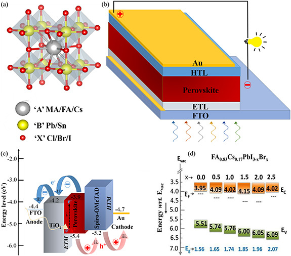
Figure 7. (a) Perovskite crystal structure, (b) schematic of the perovskite solar cell, (c) band diagram depicting working of the perovskite solar cell and (d) energy level diagram for commonly used multi-cation multi-halide FA0.83Cs0.17PbI3−xBrx (with varied Br content) perovskite absorber layer [219]. Reprinted from [219], with the permission of AIP Publishing.
Download figure:
Standard image High-resolution imageThe perovskite solar cell technology is progressing rapidly in processing large-area modules (roll-to-roll and sheet-to-sheet printing) [204] and achieving a longer lifetime, and making tandem cells with significantly higher photovoltaic conversion efficiencies [205]. Recently, Ashouri et al have reported a world record efficiency of >29% for monolithic perovskite/silicon tandem solar cells with an active area of 1.064 cm2 [205]. The significant advantage of this technology in the Indian context is that these devices can easily be used as a stand-alone system to provide rural electricity and be efficiently adapted in building integrated photovoltaic. Since perovskites is an emerging technology, it presents a prospect for India to participate in technology development and reap benefits as and when this technology matures to the level when it can get commercialized. Taking this as an opportunity, several Indian research groups have dedicated their efforts to developing stable and efficient perovskite solar cells. The significant scientific advancement in each component of perovskite solar cell technology, highlighting the Indian research community's contributions, is discussed in detail in the subsequent sections.
5.1. Improvement in perovskite absorber layer—material and morphology
The suitable pin-hole-free microstructure of the perovskite absorber layer is the foremost requirement to extract good performance from the perovskite solar cells [206]. The perovskite absorber layer thin-films are mainly deposited using solution-processed deposition techniques. The solution processability of perovskite solar cells is its most appealing aspect. This provides advantages like roll-to-roll/sheet-to-sheet fabrication, low-cost, and capital expenditure. Quintessentially, in the solution-based deposition technique, the wet liquid film is created by spin-coating/spray-deposition/drop-casting. When the liquid film dries, the solid film thermally is annealed thermally for residual solvent removal and crystallization. Despite numerous advantages, the perovskite absorber layer's deposition inherently suffers from issues like incomplete coverage and crystallographic defects [207]. These defects cause recombination, affect carrier extraction and mobility. Perovskite precursor solvent chemistry, processing condition/environment, substrate, and annealing significantly influence the perovskite crystallization kinetics and morphology [208]. Researchers worldwide have put some serious efforts into adapting numerous techniques to fabricate uniform perovskite films with optimized morphology to overcome these issues and passivate the defect states. Some of the significant developments from Indian researchers are covered in this section.
Singh et al have used 0.02 wt.% BCP additive in MALI perovskite absorber layer, which passivates and improves the quality of deposited MALI film [209]. BCP additive also acts as a moisture barrier hence improving the device stability. The device with ITO/PEDOT:PSS /MALI (with BCP additive)/PC60BM/BCP/Ag architecture has shown an efficiency close to 16% [209]. Similarly, PC70BM was blended in MALI to improve perovskite film morphology in the mesoporous device [210]. The device with FTO/TiO2/MALI (with 1 mg PC70BM)/Spiro-OMeTAD/Au architecture has shown the efficiency of 11.3%, which in the case of without PC70BM additive was 8.3%. Apart from improving the perovskite film quality, PC70BM additives also passivate the perovskite grain boundaries reducing the recombination [210]. Sharma et al reported 4,4'-Bis (N-carbazolyl)-1,1'-biphenyl (CBP) based additive for grain boundaries defect passivation of MALI absorber layer [168]. 1 mg ml−1 CBP in DMF was mixed with perovskite precursor in different ratios. 10 volume % of CBP with respect to perovskite precursor gave best results with 14.77% efficiency for the device having ITO/PEDOT:PSS/MALI (with CBP)/PC60BM/BCP/Ag architecture. CBP additives reduce the non-radiative recombination and passivate the defects [168]. The change in MALI absorber morphology with CBP additive is shown in figure 8(I), increase in CBP content beyond 20% results in formation of CBP aggregates on the perovskite surface. Sharma et al have used near-infrared NIR lamp-based radiative thermal annealing of the perovskite absorber layer [169]. The radiative heat is directly transferred to the perovskite film during NIR annealing, accelerating the crystallization process. Compared with conventional hot-plate annealing, which provides conduction-based heating, the NIR annealing method provides radiative annealing giving smooth perovskite film with larger grain size. The fabricated device with ITO/PEDOT:PSS/MALI/PC60BM/BCP/Ag has shown an efficiency of 12.33% for NIR annealed perovskite films and 10.92% for hot plate annealed perovskite films on 0.045 cm2 active area [169]. Seth and Khushalani reported the regeneration of degraded MALI perovskite absorber layer using simple one-step I2 treatment [211]. Solid iodine dispersed in hexane was drop-casted on top of degraded MALI film heated at 90 °C for 2 h. It was hypothesized that the additional input of excess I2 extracts the water from the hydrated perovskite and assists in lattice regeneration on heating [211].

Figure 8. (I) (a)–(d) FESEM image of MAPbI3 films with different CBP volume ratio (X); (e) EDX mapping of Pb for 80 vol. ration CBP and (f) XRD of MAPbI3 with CBP additive as reported by Sharma et al [168]. Reprinted from [168], Copyright (2020), with permission from Elsevier. (II) FESEM image of MALI perovskite films showing changes after solvent vapor treatment for 30 min as reported by More et al [220]. Reproduced from [220] with permission of The Royal Society of Chemistry.
Download figure:
Standard image High-resolution imageThe MALI-based perovskite absorber layer is unacceptable for practical outdoor applications with thermal and environmental instability [206]. To overcome this issue, formamidinium (FA) cation-based perovskite has been explored. Since FA cation is bigger than MA, it expands the crystal lattice, reducing the divalent cation and halide bond length and lowering the optical band-gap. The band-gap of pure MALI is 1.55 eV, and the same in FALI is 1.47 eV. The absorption onset of FALI is slightly extended beyond 800 nm compared to MALI [212], allowing light absorption in the near IR region. FALI is more thermally stable than MALI due to the stronger interaction of FA with iodine, which prevents the rupturing of the perovskite network [213]. Despite better electrical and optical properties, the pure FALI perovskite absorber layer suffers from some serious issues. One of them is the photo-inactive δ-phase. FALI has two phases at room temperature: cubic α-phase in Pm3m space group and hexagonal δ-phase in the P63mc space group. There is also a β-phase occurring at much lower temperatures −123 °C [214]. Due to the lower formation energy, the δ-phase is readily formed and is more stable; however, only α-phase is the photo-active phase and has desired optoelectrical properties [215]. Prathapani et al performed investigating microstructure and crystallization kinetics of the desired photo-active α and undesired photo-inactive δ-phase [216]. They have studied the phase evolution in two-step absorber layer deposition. It was shown that the presence of toluene in the dipping solution (8 mg ml−1 FAI in IPA with 10 vol% toluene) could moderately control the δ-phase formation [216]. Das et al reported FAPbBr3 based device using toluene as an anti-solvent. The device with FTO/TiO2/FAPbBr3/spiro-OMeTAD/Au architecture on 0.12 cm2 active area has shown the efficiency of 5.7% and 1.1% with and without anti-solvent [217].
To further improve stability and address challenges associated with δ-phase formation, mixed cation perovskite with FA/MA/Cs cations have been explored. Cs incorporation significantly improves the thermal stability and efficiency of the PSCs. Cs doping in the FALI absorber layer also stabilizes the α-phase [215], reduces the trap density and recombination, thus improving the device's performance [218]. Prathapani et al experimentally calculated the mobility, carrier density, and energy bands diagram parameters like work function, ionization energy, and electron affinity for FA0.83Cs0.17 mixed cation perovskite I–Br mixed halide system, FA0.83Cs0.17PbI3−x Brx . The fabricated FA0.83Cs0.17PbI3−x Brx absorber layer was n-type, having mobility varying from 0.28 cm2 Vs−1 for FA0.83Cs0.17PbI3 (x = 0) to 8.16 cm2 Vs−1 for FA0.83Cs0.17PbI1.5Br1.5 (x= 1.5). The electronic band structure showing different parameters extracted from UPS and UV–vis for FA0.83Cs0.17PbI3−x Brx with varying Br content is shown in in figure 7(d) [219]. As discussed previously, the precursor solvent of the perovskite absorber significantly influences the morphology and crystallinity of the layer [207]. Apart from precursor solvent, exposure of solvent vapor in the post-processing of the film also affects the perovskite absorber layer quality. These exposures can be voluntary or accidental (due to spillage or contamination from the surrounding). More et al studied the impact of various polar and non-polar solvent vapor exposure on the MALI absorber layer [220]. The top-view SEM of the perovskite film as-deposited and after solvent vapor treatment for 30 min is shown in figure 8(II). As anticipated, DMSO and DMF vapors significantly deteriorate the absorber layer due to their high polarity and Gutmann donor number. Acetone vapor has also shown a similar effect, but deterioration intensity was less due to the incapacity to dissolve Pb2+ cation. Interestingly, water vapor exposure caused less adversity than propanol. Vapors from non-polar solvents like toluene and chlorobenzene, which are generally used as anti-solvent in the two-step deposition method, help improve the film morphology [220].
5.2. Development in lead-free perovskite materials
Even though the lead-based perovskite absorber materials have achieved unprecedented success in rapid power conversion efficiency, the toxicity associated with lead has forced the research community to explore lead-free perovskite materials [221]. For the commercial acceptance of PSC technology, the problems associated with lead toxicity need to be addressed. The government of India has prohibited paints having a lead content of more than 90 parts per million (ppm) (Regulation on Lead contents in Household and Decorative Paints Rules, 2016); as of now, no such regulation exists for solar cells PSCs are in the R&D stage. Since PSCs are still in the development stage, this allows us to look for less-toxic lead alternatives for the perovskite absorber layer and safely deploy this technology for commercial applications. For excellent device performance, the selected Pb-free perovskite material must possess a high absorption coefficient, high mobility, high carrier lifetime, low exciton binding energy, and above all, good stability and low toxicity. Several elements like Mn, Sb, Ge, Bi, Ti, Cu, and Sn have been explored as Pb alternatives in the lead-free or partial lead substituted perovskite absorber layer [222–224].
Mn2+ has an ionic radius of 80 pm, much smaller than 119 pm of Pb2+, allowing Pb replacement in the perovskite crystal structure. Singh et al have partially substituted lead with manganese in MAPbx Mn1–x I1+2x Cl2–2x perovskite solar cell in ITO/PEDOT:PSS/perovskite/PC61BM/Al architecture [225]. Manganese chloride was used to substitute lead iodide, increasing the absorber layer's bandgap due to Cl substitution. Perovskite device with x = 0.8 (MAPb0.8Mn0.2I2.6Cl0.4) has shown the efficiency of 0.83%. The lower efficiency was attributed to the thinner absorber layer thickness (125 nm), limiting the photogenerated currents, thus lowering the Jsc [225]. In the later years, it was observed that additional Mn2+ assists in performance improvement, whereas substituted Mn2+ in the place of Pb2+ has detrimental effects on the performance [226].
Dey et al have modified the perovskite absorbers with triple cations B-site with doping of Group 15 (Bi) and Group 1 (K/Na) elements to achieve partial lead substituted PSCs having better moisture stability [227]. MAK0.25Bi0.25Pb0.5I3 and MANa0.25Bi0.25Pb0.5I3 was prepared having 1.86 and 1.14 eV bandgap respectively. The reported efficiency for K–Bi device is 0.14%, the same for the Na–Bi device is 0.031%. The significantly less device performance can be due to non-optimized device fabrication and the thinner perovskite absorber layer. However, bismuth insertion has shown better moisture stability for these perovskite devices even after two weeks in ambient conditions [227]. Partial substitution of lead with alkaline-earth metals (Mg, Ca, Sr, and Ba) has demonstrated enhanced structural stability compared with MAPbI3 and increased bandgap. However, with alkaline-earth metal doping, the absorption coefficient is reduced compared to pristine MAPbI3 [228]. Fully lead-free alkaline-earth metals-based perovskite materials are not suitable for absorber material, majorly owing to their wide-bandgap. Kumar et al did the theoretical simulation and experimental validation for lead-free CH3NH3BaI3 perovskite material having a high bandgap of 4 eV and high transmittance in the visible light spectrum. They have shown that La doping improves its conductivity, making La-doped CH3NH3BaI3 a potential candidate for transparent conductor applications [229].
Bismuth and antimony, group VA elements neighboring to lead, have also been explored widely for the lead-free perovskite absorber layer. Since they are trivalent cations (having three electrons in the outermost shell), they form 'B'X6 3− (B = Bi or Sb) octahedron bonds with halides 'X' (Cl, Br, I), which coordinates with MA/FA/Cs cations, this coordination spawns different phases and dimensions like 2D A3B2X9 and 0D A3BX6. A3B2X9 is the most adapted structure for Bi, Sb perovskite absorber layers. Paul and Pal have reported lead-free antimony-based perovskite solar cells; MA3Sb2I9 perovskite absorber layer with Cl incorporation was used [230]. Cl addition assists in achieving the defect passivated 2D-perovskite phase. The fabricated p-i-n device with ITO/Cu@NiO/MA3Sb2Clx I9–x /ZnO/Al have shown the best efficiency of 1.55% for x = 0.3 [230]. Ahmad et al have used the modified two-step deposition method for MA3Sb2I9 based absorber layer deposition [231]. In the first step, the SbI3 precursor is spin-coated and kept in the chlorobenzene vapor environment. In the second step, the prepared film was dipped in an MAI solution. No residual peaks of MAI and SbI3 were observed in the XRD analysis of film prepared using the two-step method; these residual peaks were present in the film prepared with the one-step method, suggesting incomplete crystallization. The overall film morphology was also better for the absorber layer prepared with the two-step method. The FTO/CL‐TiO2/m‐TiO2/MA3Sb2I9/ spiro-MeOTAD /Au based devices have the best efficiency of 0.54% with encouraging Voc of 740 mV [231]. Waykar et al have synthesized Cs3Bi2I9 films having a bandgap of 2.1 eV and high thermal stability up to 420 °C [232]. The fabricated device with AZO/C-TiO2/Cs3Bi2I9/CuSCN/graphite architecture has shown an efficiency of 0.17% [232].
Sn-based perovskites have shown promising potential among all lead-free alternatives, with less toxicity and a favorable bandgap of 1.2–1.4 eV with excellent optoelectronic properties. The ionic radius of 118 pm of Sn2+ is very close to 119 pm of Pb2+. With various composition engineering, Sn-based, Pb-free PSCs have reached the efficiency of 12.4% in 2020 with (PEA)0.15(FA)0.85SnI3 doped with 0.075 M SnF2 and 0.05 M NH4SCN [233] from the first report with MASnI3 absorber layer having 6% efficiency in 2014 [234]. To date, Sn-based perovskites are far ahead from the other Pb-free perovskite materials, but it faces some critical issues which need to be addressed. Sn-based perovskite absorber material rapidly oxidizes from Sn2+ to Sn4+, making device fabrication and characterization difficult outside the glove-box environment. Another challenge is controlling the morphology and crystallization. The effect of anti-solvent and SnX2 on the film morphology of FASnI3 was studied by Aftab A. and Ahmad I [235]. A 10% SnF2 and 10% SnCl2 additive were used as a reducing agent, which improves the film morphology. Absorber layer film with chlorobenzene-based anti-solvent had better morphology compared with toluene [235]. To compete with Pb-based perovskites, Sn-based perovskite still requires intensive research focused on defects and morphology control along with ways to suppress the oxidation.
5.3. Electron and hole transport materials for PSCs
The perovskite absorber layer is sandwiched between the ETLs and HTLs in the typical perovskite solar cell device architecture. The primary role of these layers is to collect the photogenerated charge carriers (electron and holes) and facilitate their transport to the respective electrodes. TiO2 and Spiro-MeOTAD (2, 2', 7, 7'-Tetrakis-(N, N-di-4-methoxyphenylamino)-9, 9'-spirobifluorene are the most commonly reported electron and hole transport materials respectively. However, to enhance device stability and efficiency, several other materials have been explored.
5.3.1. Electron transport materials (ETM)
TiO2 is the most widely used ETM. It provides promising properties like high optical transmittance, electron lifetime, and favorable band alignment. However, it also suffers from some drawbacks like a high trap density, low electron mobility (0.1–4 cm2V−1s−1) [236] than perovskite electron mobility (10–35 cm2V−1s−1) [237]. Conventional TiO2 based ETM also impedes device stability under light illumination. Adhikari et al demonstrated that an optimum grain boundary potential and proper band alignment between the TiO2 ETL and perovskite absorber layer help increase overall device performance [238]. Ranjan et al reported the conductivity enhancement of TiO2 by tantalum (Ta) doping and its effect on improving the device performance (PCE of 9.24%) [239]. Downward shifting of the TiO2 fermi level by Ta doping provides the driving force for the electron transfer from perovskite LUMO level to TiO2 conduction band [239]. To overcome the problems associated with TiO2, several other ETM have been explored. Subiah et al deposited ZnO by RF magnetron sputtering on perovskite absorber FA lead tribromide (FAPbBr3) layer as an ETL in p-i-n architecture [240]. These devices showed PCE 8.3% and better stability under continuous illumination than conventional organic ETL (PCBM)-based devices. The ZnO layer being inorganic minimized the degradation process in ambiance [240]. Subiah et al compared the performance of ALD–Nb2O5 with existing ETL like PC60BM, TiO2 in planar PSCs. The ALD-Nb2O5 (PCBM)-based devices showed more negligible hysteresis, better stability, and robustness [241]. In another work, Subiah et al reported methodology to fabricate compact SnO2 ETL by sol-gel method and employing low-power N2 and N2O RF plasma post-treatment. The devices exhibited PCE of 20.3% on FTO and 18.1% on the flexible substrate [242].
For inverted architecture, where ETM needs to be deposited on top of the perovskite layer, PCBM is most commonly used due to its high electron mobility and electron affinity. However, PCBM is expensive and has ambient instability due to the presence of a hydrophobic ester group. Several other alternatives for PCBM have been explored. Sharma et al demonstrated air-stable diketopyrrolopyrrole-based (TDPP-CN4) molecule as ETL for inverted architecture [243]. However, owing to the deep LUMO level, the prepared devices with TDPP-CN4 ETL have shown significantly inferior performance (3.53% efficiency) compared with conventional PCBM ETL-based devices (11.2% efficiency) [243]. Shaikh et al proposed the design and synthesis of dithiafulvenyl (DTF)-naphthalenediimide (NDI) based small molecule derivatives as non-fullerene ETL and achieved the highest PCE 11.4% [244]. It was envisaged that two dithiol units at the NDI core decrease the energy band gap and provide more sulfur atoms to bind the perovskite layer via S–I and S–Pb binding [244].
5.3.2. Hole transport materials (HTM)
Conventionally, Spiro-OMeTAD (2, 2',7, 7'-Tetrakis-(N, N-di-4-methoxyphenylamino)-9, 9-spirobifluorene) is used as HTM in n-i-p architecture of PSCs due to its suitable ionization potential, absorption spectrum, solubility and solid-state morphology. The synthesis cost, complex multi-step processing, ambient instability, and hygroscopic dopants requirement put limitations for robust massive application of Spiro-OMeTAD as HTM in PSCs. It paves the quest for searching and developing other efficient and inexpensive molecular HTMs with optimal energy levels and suitable optoelectronic properties. Pratyusha et al discussed about using pristine PCDTBT ([Poly[N-9'-heptadecanyl-2, 7-carbazole-alt-5, 5-(4',7'-di-2-thienyl-2', 1', 3'-benzothiadiazole)] and PCDTBT doped with PCPDTBT([Poly(4, 4-bis(2-ethylhexyl)-cyclopenta-[2, 1-b;3, 4-b]dithiopene)-2, 6-diyl-alt-2, 1, 3-benzothiadiazole-4, 7-diyl]) as HTM [245]. The highest efficiency of 4.35% was reported using PCDTBT as HTM [245]. Srivastava et al reported the use of polymers PBDT-DFBT and PF-DTDFBT along with spiro-OMeTAD. Polymer/spiro bilayer HTM devices show a higher VOC 1.09 V than that of spiro-OMeTAD devices. PSCs with polymer/spiro bilayer HTL show PCE of 13.91%, while spiro-OMeTAD devices showed PCE of 13.4% [246]. Reddy et al reported synthesizing hydrophobic and conductive porphyrin derivatives using N-octyl phenothiazine as donors and porphyrin as π-spacer in a D-π-D configuration [247]. Phenothiazine-porphyrin functionalized with alkyl chains, namely 3, 3'-((10, 20-bis(2, 6-bis(octyloxy)phenyl)porphyrin5, 15-diyl)bis(ethyne-2, 1-diyl))bis(10-octyl-10 H phenothiazine) (HPPHT), and 3, 3'-((10, 20-bis(2, 6-bis(octyloxy)phenyl)porphyrin-5, 15-diyl)bis(ethyne-2, 1-diyl))bis(10-octyl-10 H-phenothiazine)-Zn(II) (ZPPHT) were synthesized and used as HTMs in PSCs. Screen-printed ZPPHT based perovskite solar cells with carbon nanoparticle graphene composite as a CE exhibited a PCE of 11.26% compared with a PCE of 9.47% for HPPHT 8.84% for devices without HTMs [247]. Sathiyan et al reported the synthesis of two donor-acceptor-donor type HTMs (TTz-1 and TPDCN), with a triphenylamine donor unit with electron-deficient centers of dicyanovinylene and thiazolo[5,4-d]thiazole [248]. The hydrophobic nature and highly ordered conjugation of TTz-1 and TPDCN devices showed substantially improved device stability than the Spiro-MeTAD-based device. The PSCs devices fabricated using TTz-1 as an HTM yielded PCE of 11.37%, while devices using TPDCN show a PCE of 10.11%, comparable to the PCE of 11.62% with conventional spiro-MeTAD-based HTM [248]. Yadagiri et al reported the synthesis and characterization of a dithienogermole (DTGe) based small molecule named Ge-PO-2CN as dopant-free HTM for PSCs [249]. Inexpensive and easy processing techniques were used to synthesize this molecule. It consists of a high planar and electron-rich DTGe core as a central core unit covalently linked with an electron-rich phenoxazine group that was capped with an electron-deficient malononitrile group. PCE of up to 11.63% is achieved using Ge-PO-2CN as HTM on the area of 1.02 cm2 [249].
Apart from the above-discussed developments in organic HTMs, inexpensive and stable inorganic materials have also been extensively explored as HTMs. Subiah et al reported NiO and CuSCN as potential HTMs for planar, inverse CH3NH3PbI3−x Clx -based cells. The NiO-based device showed an efficiency of 7.3%, while CuSCN based HTM increased devices up to 3.8% in efficiency [250]. Murugadoss et al also reported doctor-bladed CuSCN based HTM for PSCs, and the best performing device has shown 10.07% efficiency [251]. Chaterjee et al introduced Cu2O as HTM inverted planar structure and compared its performance with NiO and Cu@NiO-based devices [252]. The Cu2O layer was fabricated through the SILAR method. The best performing device with Cu2O /MAPbI3/PCBM architecture has shown an efficiency of 8.23% [252]. Patel et al proposed the use of sol-gel synthesized nanoparticles of CZTS as inexpensive HTM for PSCs. The combination of CZTS nanoparticles and SnCl2-doped perovskite CH3NH3Pb1−x Snx I3−y Cly (CZTS-PVSK) was reported efficiently 9.66% [253]. Tamilselvan et al discussed the synthesis of copper antimony sulfide (CAS, Cu12Sb4S13) tetrahedrite crystal phase nanoparticles capped with organic ligands using the hot injection method [254]. The hydrophobic nature of CAS leads to chemical stable and moisture resistant devices. Devices with CAS as HTM showed a significant delay in device degradation than the spiro-OMeTAD based device [254].
5.4. Counter electrode materials for PSCs
The CE is an integral part of the PSCs, having the primary role of electron/hole collection. A transparent electrode (FTO or ITO) on one end of the PSCs on which all the other layers are deposited sequentially is conventionally termed the working electrode. The light falls on the device from this end. The CE is deposited at last and is also known as the back electrode. Au and Ag are the most commonly used CE materials in PSCs. They have excellent electrical conductivity and work-function matching with the perovskite absorber material and HTM. Even though most of the highest reported efficiency of PSCs is with Au-based CE, they have some severe drawbacks. Au can diffuse through HTL and react with the halides present in the perovskite absorber layer; Au + 2I− → 2AuI2 − + e−, creating a metal-halide barrier. This reduces the stability of the device [255, 256]. Since Ag has a lower standard electrode potential than Au, it makes more havoc on the device stability [257]. Apart from metal migration problems and cost, the metal CE deposition requires vacuum processing techniques that limit its scalability and roll-to-roll production.
Carbonaceous materials like carbon black, CNTs, graphite, and graphene are the front runners replacing Au/Ag as the CE in the PSCs. They show excellent properties, i.e. good conductivity, high stability, chemically inertness, solution processability, and above all, the suitable work function of 5 eV [258]. The carbon-based perovskites can be fabricated in two architectures: monolithic mesoporous architecture (FTO/TiO2/ZrO2 or Al2O3/carbon and perovskite is infiltrated from top of the carbon layer) and layer-by-layer architecture (FTO/TiO2/perovskite/carbon). ZrO2 or Al2O3 is used as the separator layer to separate ETL (TiO2) from the carbon layer in the mesoporous architecture (figure 9(a)). The screen-printed device before perovskite infiltration is shown in figure 9(b). These devices are mostly HTM free, and there is a considerable energy gap between the work function of carbon (−5.0 eV) and the valance band of MALI (−5.4 eV); this gap obstructs the efficient charge extraction. In the mesoporous architecture, the carbon layer typically requires high temperature (usually 400 °C) sintering to burn solvent and binders. Dileep et al proposed preparing room temperature curable carbon electrodes [259]. Carboxy-methylcellulose-based binder with water as solvent was used to prepare the carbon paste. For the device fabrication, TiO2 and ZrO2 were spin-coated and sintered sequentially. After that PbI2 was spin-coated before screen-printing of the carbon paste, and finally, the substrates were dipped in MAI solution for perovskite (MALI) phase formation. The prepared device has shown the efficiency of 9% [259]. The mesoporous architecture of carbon-based perovskite devices offers several advantages like less perovskite precursor wastage, ambient processing, and improved stability due to the hydrophobic nature of carbon [258]. However, in this device architecture, drop-casting of perovskite precursor causes non-uniform infiltration and crystallization [260]; also, the use of a thick separator layer induces additional RS losses [261]. The layer-by-layer architecture, where the device fabrication sequence is similar to the conventional Au/Ag-based device. The schematic for the layer-by-layer architecture of carbon-based PSC is shown in figure 9(c). This architecture solves some of the problems associated with MC-based PSCs, like eliminating the use of an additional separator layer and the potential for low-temperature processing. This architecture with P3HT-graphene as HTL (FTO/SnO2-TiO2/FA0.3MA0.7PbI3/P3HT-graphene/carbon) device have shown the efficiency of 18.2%, which is the highest efficiency for carbon-based PSCs [262]. In layer-by-layer architecture, the carbon layer is deposited after the perovskite layer; hence the carbon layer must be processed below 150 °C. This makes the binder selection crucial, as most organic binders will not burn out completely at this temperature. Considering this, Kartikay et al have studied the effect of carbon paste binders on the perovskite absorber layer [263, 264]. They have prepared nine sets of carbon pastes with three different binders (ethylcellulose, polyvinylpyrrolidone (PVP), and PMMA) and three different solvents (chlorobenzene, toluene, and terpineol) [264]. The device was fabricated with FTO/TiO2 CL/TiO2 ML/FA1-x MAx PbI3-y Bry /carbon architecture; the cross-section SEM showing the interfaces is shown in figure 9(d). PSC with PMMA-chlorobenzene based carbon paste gave the best results with 10.74% efficiency. It was reported that the PVP binder causes initial degradation of the perovskite absorber layer due to the hydrophilic nature of pyrrolidone. The remaining all devices have demonstrated considerable stability. The device with PMMA toluene-based carbon paste shows a T80 of 480 h [264]. The further improvement in device performance was reported by adding functionalized NiOx and CNT (f-NiOx + CNT) as HTM layer [265]. The room temperature processable and perovskite compatible f-NiOx + CNT HTM was reported by Kartikay et al The addition of the HTM layer improves efficiency from 8.67% to 11.36%, and the large-area series-connected device with 4 cm2 active area have shown 6.11% efficiency. The schematic of the device and cross-section SEM image are shown in figures 9(e) and (f) [265].

Figure 9. (a) Device structure of monolithic-MC-based perovskite solar cell; (b) typical screen-printed carbon device before perovskite infiltration; (c) schematic of the layer-by-layer architecture of carbon-based PSC and (d) FESEM image is showing different interfaces [264]. Reprinted from [264], Copyright (2020), with permission from Elsevier. (e) Schematic of series connected device and cross section SEM image of the device with f-NiOx + CNT HTM layer [265]. Reprinted from [265], Copyright (2021), with permission from Elsevier.
Download figure:
Standard image High-resolution image
Overall, carbon provides an excellent alternative to conventional Au/Ag-based PSCs and has shown better stability. But there are some issues like the poor interface between the perovskite absorber layer and the carbon layer; mismatch in energy levels. Above all, the carbon layer is susceptible to scratches. These issues need to be addressed to take a positive leap towards the mass production of carbon‐based PSCs and commercialization. We have presented the inclusive summary of gradual developments by the Indian research community and challenges in various aspects of perovskite solar cells. With the rapid advancement in perovskite solar cell fabrication, numerous commercial firms are involved in perovskite solar cell fabrication with efficiency and scalability. Even though this technology is not available in the common market, various stakeholders have demonstrated large-area and efficient perovskite solar cells. South Korea-based frontier energy solution has demonstrated 20% efficient 225 cm2 modules [130]. UK-based Oxford PV has certified 28% perovskite-silicon tandem solar cells on 1 cm2 cell [130]. Other companies like Microquanta Semiconductor, Saule Technologies, Swift Solar, etc, work on various aspects of perovskite solar cells, including flexible and roll-to-roll production [130]. But there are still many issues with the commercialization of perovskite solar cells, like lead toxicity and stability. There is no standard of testing stability of perovskite solar cell like IEC 61 215 for Si solar cell, which involves heating modules at 85 °C for 1000 h at 85% humidity. PSCs would first have to achieve stability of minimum few years to attain the success of silicon-based solar cells. Up to this point, though, such a target seems to be very far off, given that even most of the lab-scale devices have not yet achieved this stability level.
6. Energy storage devices
6.1. Batteries
A battery is an energy storage device that involves converting chemical energy into electrical energy through electrochemical oxidation-reduction reactions [266]. In general, a battery consists of one or more electrochemical cells connected in series/parallel depending on the required output capacity and voltage [267]. The electrochemical cell consists of three major components: anode, cathode, and electrolyte [267]. The anode (negative electrode) acts as a reducing agent, while the cathode (positive electrode) acts as an oxidizing agent, stable when in contact with the electrolyte, and desires working voltage [267]. The electrodes should have good electrical conductivity, structural stability, and low cost. The electrolyte must have good ionic conductivity, which provides the medium for transporting charge carriers inside the electrochemical cell between the positive and negative electrodes [267]. The batteries are classified into primary and secondary batteries. Primary batteries are non-rechargeable batteries, and secondary batteries are known as rechargeable batteries [266]. Lead-acid, nickel-cadmium, nickel-metal hydride (NiMH) are rechargeable batteries available in the market for many applications [266]. However, these batteries exhibit low gravimetric energy, high internal resistance, memory effect, longer charging time, and high self-discharge rate (40% per month) [266].
LiBs are rechargeable batteries. The basic working principle of LIBs is that Li+ ions migrate between the positive and negative electrodes through the electrolyte [268]. During discharging process, Li+ ions migrate from the anode through the electrolyte to the cathode and insert into the cathode [268]. At the same time, electrons from the anode are transferred through an external circuit to the cathode [268]. This process is reversed during charging. These LiBs have many advantages such as high voltage (3.3–3.8 V), high energy density (250–730 WhL−1), specific power (approximately 250–340 Wkg−1), self-discharge rate (5%–10%), superior rate capability, long cycle life and operation over a wide temperature range (−20 °C to 70 °C [269]. Owing to these attractive properties, LIBs have been utilized in many applications such as electronic gadgets (mobile phones, laptops, and cameras), military, satellites, and others [269]. Commercial LiBs dominate the global market share up to 63%, 23% for NiCd, and 14% for NiMH batteries, respectively [269]. However, the existing state-of-the-art LiBs slowly reach their topotactic chemistry limitation, which impedes energy and power density enhancement [270]. Due to the lack of Li metal distribution globally, its high cost has been a driving force for researchers to explore beyond the current state-of-the-art LIB technology for large-scale applications of electric mobility and stationary power storage devices [269–271]. Nevertheless, in the search for batteries with high volumetric capacities and increased gravimetric/volumetric energy densities for transport sectors and stationary storage applications [269–271]. Among the research community in India and worldwide, novel electrode development is the main focus of interest for better device performance with superior alternative battery technologies for future large storage systems and other applications.
Currently, graphitic carbon is used as an anode material in commercial LIBs. It has a typical layered structure of stacked graphene sheets, which facilitate the movement of lithium ions in and out of the host structure during intercalation/de-intercalation in a reversible way. The graphitic carbon theoretical specific capacity is 372 mAh g−1 with the formation LiC6 at a potential below 0.3 V. Graphitic carbon undergoes 10% volume expansion during Li intercalation/de-intercalation [272–274]. However, disadvantages of using graphite are relatively low specific capacity (372 mAh g−1) and dendrite formation on the graphite's surface due to volume expansion, especially at the high charge/discharge rates [274, 275]. Several research groups from India are focusing on developing high-performance anode materials such as carbon-based materials (graphitic carbon, CNTs, graphene, RGOs, and carbon derived from solid wastage), metallic (Sn, Al, Si, Sb, and Al), metal sulfides/selenides (MSs), sulfide, MOs, MXenes, metal-organic frameworks (MOFs), and perovskites and their hybrid electrodes are investigated for LiBs [275–288]. The metals-based electrodes suffer from capacity fading and poor cyclic performance, primarily due to the volume changes during electrochemical cycling (viz., Li-alloying/de-alloying). The large volume changes in electrode materials during lithium insertion/extraction generate stresses, which induce cracking and loss of electrical contact between the active material and current collector. Accordingly, the major challenge for implementing alloy anodes is the significant structure and volume changes during lithium insertion and extraction, leading to pulverization of the active alloy particles and extremely poor cyclability [287]. The hybrid electrode-based MoS2/CoMoO4 nanoarchitectures were used as a stable anode for high-performance LIBs [289]. The MoS2/CoMoO4 electrode-based LiBs delivered a high discharge capacity of 600 mAhg−1at the current rate of 5 C after 500 electrochemical cycles with high columbic efficiency. The researchers are putting effects on further improving the energy and power density via developing the hybrid anode and cathode materials (CMs)for LiBs.
6.1.1. Cathode materials
Lithium layered oxides (LiMO2, M = Co, Ni, and Mn) are CMs for LIBs, exhibiting specific capacities ⩽160 mAh g−1 with an upper potential limit of 4.3 V versus Li [267, 268]. LiCoO2 mainly uses standard CM in commercialized LIBs and has not been considered for electric vehicle application due to high cost, low thermal stability, fast capacity fading at high current rates [268]. LiMnO2 is reported as cost-effective material; however, low electrochemical performance at high temperatures indicates the necessity of developing other layered CMs [268]. The mixed transition-metal layered oxides (xLi2MnO3·(1–x)LiMO2 (M = Ni, Mn, Co) are reported as promising CMs for LIBs due to their high specific capacity (∼195 to ∼250 mAhg−1) [267, 268, 290]. The electrochemical properties of LIBs can be further improved by controlling the chemical composition, morphology, and specific surface area of these CMs [290]. However, these materials suffer from capacity fading and discharge voltage decay upon cycling [290]. An alternative, olivine-structured lithium transition metal phosphates and silicates (LiMPO4, LiFePO4, and LiMSiO4) are considered CMs, because of their low cost, non-toxicity, and better stability [291]. However, these metal phosphates and silicates-CMs based LIBs exhibited poor electrochemical performance ascribed to low electronic conductivity [291]. Carbon coating and metal doping to phosphates/silicates help to enhance the electronic conductivity and electrochemical performance [292]. The problems associated with CMs can be minimized by further treatments like surface coating (via gas treatments, ALD, wet chemical means), doping of cations, using surface-active additives in the electrolyte solutions, controlling the activation process by temperature, and other [290, 293]. Intensive research activities have been carried on these CMs, and they are still considered very important for advanced, high-energy-density Li-ion battery technology [290, 293]. Hence, the authors could only provide an idea about the scope of relevant efforts invested toward their stabilization during prolonged cycling.
6.1.2. Novel competing battery technologies
Recently, several alternative battery technologies such as sodium-sulfur batteries (SIBs), Zn ion—batteries, Li-sulfur batteries, Li-air batteries, Iron-ion battery, Ca-ion battery full cell have been under investigation for high gravimetric/volumetric energy densities devices for future electronic gadgets, transport sectors, stationary storage, and other applications [270, 294–299]. Among these batteries, SIBs are cost-effective and an alternative for LIBs in portable, large-scale renewable energy storage applications due to abundant sodium and similar electrochemical mechanisms [300, 301]. However, the lack of an appropriate anode (a stable anode), low capacity, and sluggish mass transport have hindered the commercialization of SIBs [301, 302]. Several materials such as TMOs, transition metal sulfides, carbon materials, transition metal phosphides, MXenes, and transition metal carbides have been investigated as anodes for SIBs owing to their abundance, cost-effectiveness, and high theoretical capacity [300–305]. However, these materials have insufficient electrical conductivity, a large volumetric change during electrochemical cycling, detrimental rate capability, and cycle stability [300–305]. Incorporating carbonaceous materials such as CNT, graphene, and 3D porous carbon into these transition metal compounds and other functional materials can improve the functionality of SIBs electrodes [302, 303]. The carbonaceous materials effectively prevent the agglomeration of anode materials during electrochemical cycling and the enhanced electrical conductivity, resulting in the enhancement of the rate capability and cycle stability of hybrid materials-based anodes [302, 303]. All other emerging battery technologies are in the initial stage of fabrication, characterization, and investigation of the charge storage mechanism.
Various batteries are commercially manufactured to fulfill the everlasting demand for consumer applications and an imminent surge in demand in electronic vehicles (EV). LiBs, commercialized in 1991 by Sony, is the most commercialized and used battery technology [293]. However, it has been estimated that due to higher EV deployments, the Li demand for batteries will rise from 0.036 to 0.77 Mt [306]. Apart from LiBs, various Zn-based batteries being commercially produced. US-based Imprint energy has commercialized ZincPoly™ technology which is ultrathin screen-printed flexible Zn–MnO2 batteries. Blue Spark Technology has also commercialized flexible Zn–MnO2 batteries. These technologies still require more developments for wide-scale applicability. Other than Zn–air batteries, Mg–air batteries can also be a viable alternative for LiBs. With the implementation of the National Mission on Transformative Mobility and Battery Storage by the Government of India in 2019, giga-scale battery manufacturing in India is aimed. The in-depth strategic perspective of battery manufacturing in India can be found in [307].
6.2. Supercapacitors and hybrid energy storage
Supercapacitors are electrochemical energy storage devices classified into three types based on their charge storage mechanism: electrochemical double-layer capacitors (EDLCs), pseudocapacitors, and hybrid capacitors [308]. The charge-storage mechanism in EDLCs is based on the interfacial electrostatic separation or non-faradic process; there is no transfer of charge between electrode and electrolyte [308]. In pseudocapacitors, the charge storage mechanism is based on the faradic process through the transfer of charge between electrode and electrolyte [308]. Due to the Faradaic processes, pseudocapacitors give better capacitances and energy densities than EDLCs [308]. Hybrid capacitors utilize both Faradaic and non-Faradaic processes to store charge [309]. SCs are gaining interest in the modern smart world because of their outstanding properties like rapid charge–discharge rates, long cycle life, high power delivery, and cycle efficiency [309, 310]. Although SCs show high power density (1000–2000 Wkg−1) and extreme long cycles (>105 cycles), they comparatively dispense low energy density (1–10 Wkg−1) than batteries (20–100 Wkg−1)[310]. The electrode and electrolyte materials play a vital role in improving supercapacitor energy density and stability, enhancing devices' life span and performance [309]. The high-performance supercapacitor electrode materials should have cost-effective, good electronic and ionic conductivity, large specific surface area, temperature stability, porous morphology (distribution of pores with optimized size), convenient processing, good corrosion resistance (chemical stability), and mechanical stability [309, 310]. The selection of suitable materials and their optimized design for electrodes are key strategies to make supercapacitors more prominent energy storage devices than batteries [310]. Several materials such as carbonaceous materials (graphene, CNT, activated carbon, and carbon derived from the solid waste), MOs, metal hydroxides (MOHs), MXenes, MOFs, metal nitride (MNs), metal sulfides/selenides (MSs and layered sulfides), CPs, metal oxynitrides (MONs) and perovskites have been explored for electrodes for SCs applications [279, 309–316]. The carbon materials and MONs exhibit EDLC behavior, and non-carbon materials (MOs, MOHs, MOFs, MSs, and perovskites et al) show pseudocapacitive/ Faradaic mechanism [310]. In addition to the difference in a storage mechanism, there is substantial variation in cyclic stability and rate capabilities based on the carbon and non-carbon electrode materials used in SCs [310]. For example, carbonaceous materials (graphene, CNT, activated carbon) show high cyclic stability (>105 cycles). However, they are suffering from low capacitance values (∼250 F g−1), and hence the energy density associated with these devices is less [310]. Similarly, MOs have high capacitance values (∼720 F g−1 for hydrous ruthenium oxide), and the energy density associated with these materials is high. However, MOs suffer from poor electronic conductivity (10−5–10−6 S cm−1) and cyclic stability (<104 cycles), which limits practical applications [310]. These aspects point out the technological gap as far as materials for high-performance SCs are concerned. All these insights indicate that hybrid electrode materials, such as combination of non-carbon materials—carbon materials (BFO/rGO, ZIF-67/rGO), sulfides/oxides, MOFs/sulfides (ZIF-67/Co3S4), sulfide/MXenes (MoS2/MXene) and others enhanced SCs performance [279, 309, 315–320]. The hybrid electrode materials emphases on optimization of electrical and ionic conductivity, structural flexibility, charge carrier mobility, more porous active sites, and other parameters that improve supercapacitor performance.
The strategic method is to increase energy and power density by hybridizing LIBs and supercapacitors (hybrid energy storage devices) to overcome individuals' limitations [321–323]. LIBs contain an intercalation-type anode (high capacity battery anode) to provide high energy density combined with the porous cathode (activated carbon or porous carbon as the cathode) to deliver high power density [323–325]. By utilization of hybridization concept, Li-ion capacitor can store charge by reversible lithium intercalation/de-intercalation at the anode and adsorption/desorption on the surface of the cathode side [323–325]. Padya et al reported porous nitrogen-enriched carbon as anode and nanoscale graphene as cathode for Li-ion capacitor with discharge capacity of 147.9 mAh g−1 at a current density of 1.0 A g−1 with a capacity retention of 94.2% after 500 electrochemical cycles [326]. Sodium vanadium phosphate as anode with activated carbon as bi-material cathode used for hybrid battery-supercapacitor [327]. Sodium-ion capacitors with Na2Ti2O4(OH)2 as anode and rice husk derived porous carbon as cathode exhibited the energy density of ∼65 Wh kg−1 [327] and V2O5 anchored rGO (as the anode) with honey derived activated carbon as cathode delivers the energy density of ≈65 Wh kg−1 [328]. Potassium ion capacitor with potassium niobate (K4Nb6O17, KNO) nanosheet arrays as anode and orange-peel derived activated carbons cathode delivers high energy density of 116 Wh kg−1 [329]. Hybrid high power density and long cycle stability can become the ultimate power source for multi-function electronic equipment and electric/hybrid vehicles.
6.3. Bifunctional devices
The bifunctional photo-powered energy devices (PPEDs), which merge the energy conversion and storage in a single device, satisfy a convenient power supply [330–332]. For example, the integration of solar energy converting device with a supercapacitor in a single device is called a photo-supercapacitor [331]. The dual-functionality of photo-supercapacitor is drawn much attention towards future portable and wearable applications [331]. The figure of merit of photo-supercapacitor is the energy conversion and storage efficiency (ECSE) over a complete charge–discharge cycle [333]. The current development of the photo-supercapacitors is still in the early stage and mainly focused on integrating the various electrode materials (carbons, conductive polymers, MOs, and others) of the supercapacitors with the different types of solar cells (DSSCs, polymer solar cells, quantum dot DSSCs (QDSSCs), and perovskite solar cells) into single dual-functional devices [330–332, 334, 335]. For example, Das et al have demonstrated the proof of concept integration of the CdS quantum dots based QDSSCs combined with the supercapacitor (figures 6(k) and (l)) [334]. CdS quantum dots/hibiscus (hb) dye co-sensitized TiO2 was utilized as the solar cell. Poly(3, 4- ethylenedioxypyrrole) (PEDOP)@MnO2 was utilized as the CE for the solar cell as well as the electrodes for the symmetric supercapacitor [334]. The photo-supercapacitor exhibits a specific capacitance of 183 Fg−1, an energy density of 13.2 Whkg−1, and a power density of 360 Wkg−1 at a discharge current density of 1 Ag−1 [334]. The fabricated photo-supercapacitor with the PEDOP@MnO2 CE using an aqueous polysulfide–silica gel electrolyte demonstrated an efficiency of 6.11% [334]. Further improvement in the performance of PSCs can be possible by optimizing the PCE, FF, capacitance, light intensity, time constants, series, and shunt resistances [330–334, 336]. The feasibility of fabrication various architectures of PSCs has been demonstrated; however, they inevitably have some problems and challenges such as low charging voltage, self-discharging, and ECSE, the difficulty in encapsulation, and non-standardized evaluation on the performances for photo-supercapacitors [330, 331]. Thus, further research must focus on overcoming the existing obstacles and the fabrication of new prototypes. Despite the numerous challenges in the photo-supercapacitor, authors believe that the photo-supercapacitors have a bright future in a broad spectrum of applications. The advances made in the development of the photo-supercapacitors will eventually allow them to be applied in our daily lives, particularly portable and wearable devices.
7. Conclusions and future scope of work
In this paper, we have systematically discussed the journey of solar PV and related materials research in India. Research and developments of energy materials are significantly visible with numerous research publications over the years. Although there has been significant development in all photovoltaic technologies by the Indian research community over the years, most of the research is still at the lab-scale except Si solar cells. India is aggressively pursuing Si solar PV installation to generate clean energy and reduce its carbon footprint. This transition to renewable energy resources will also uplift socio-economic growth. Currently, solar module production capacity in India can only meet 35% of the total annual domestic demand, and the remaining 65% of solar panels are importing from foreign countries. India imports almost all machinery, raw materials, and components, contributing to the high cost of solar modules. Immediate attention and suitable policy must provide the necessary impetus to bring technologies for raw materials development and scale-up solar module production capacity to meet domestic demand.
Intensive research progress has been made in all the energy storage technologies by the Indian research community and established energy storage facilities. However, it currently lacks a central framework to standardize energy storage systems. The Indian government set a road map for energy storage systems from 2019 to 2032 with India smart grid forum (ISGF). In association with the Indian energy storage alliance (IESA), ISGF has estimated energy storage requirements for different portable electronic applications for 2022, 2027, and 2030. The IESA has estimated over 70 and 200 GWh of energy storage capacity in India by 2022. The need for a clear-cut policy and regulatory framework for energy storage, similar to India's policy on renewable energy, plus investment incentives, improved storage technology, and realistic targets for developing storage capacity.
Third-generation solar PV and supercapacitors are emerging technologies, which are yet to mature and are not yet fully commercialized. These areas provide the opportunity to excel in technological developments and reap benefits as and when these technologies are commercialized. Combative research and required industrial collaboration will offer the opportunity to be self-reliant. Apart from the development of new energy materials, we should also look for solar module recycling. The majority of Si-solar cells have a lifetime of 25 years, and considering the rapid solar module installations from the early 2000s, these modules are set to reach the end of life in the coming years. Research for the efficient recovery and safe disposal of modules is the need-of-hour. A fundamental understanding of solar cells and their modules fabrication, characterization, energy conversion, and storage devices is well matured in the Indian research community. However, the following research areas need further development: (a) improving the performance and stability, (b) large-area devices, (c) flexible and wearable devices, (d) transparent devices, and finally (e) integration of energy conversion and storage devices.
In this regard, the following approaches may be pursued:
- The combinational approach for faster identification of optimal processing conditions has been well implemented for light absorber layers, the buffer layer, and transparent electrodes in TFSCs (CIGSe, CZTSe) [82, 105, 106]. A similar approach may be adopted to rapidly screen emerging absorbers and other components for perovskite and other third-generation PV technologies.
- The perovskite solar cell has reached 25% efficiency with the FAPbI3 absorber layer [203]. But due to Pb toxicity, special attention is needed to develop Pb free–light absorbers without compromising stability and efficiency.
- Perovskite solar cells' efficiency and stability can be improved by embodying core/shell Au/CZTS nanoparticles in the CH3NH3PbI3−x Clx absorber [337]. For instance, with the incorporation of optimum concentration of Au/CZTS NCs in perovskite absorbers, PSCs have achieved a higher efficiency of ∼20% and long operational stability (800 h) [337]. The incorporation of other earth-abundant absorbers in perovskites can be explored to enhance PSCs' performance and stability. Tandem solar cells are also an up-and-coming option.
- The life span of PSCs depends on the interface's stability (top electrode or bottom electrode/adjacent layer, absorber/ETL or HTL), the stability of individual layers and hygroscopicity, thermal instability, and ion migration in the devices [338–340]. The particular focus on stable electrodes, ETL, HTL, absorbers, and the deposition of external protection PMMA, CYTOP layers are required to improve PSCs' stability. The same concept applies to other third-generation solar cells.
- The highest efficiency of 13.8% and 7.4% have been reported for CIGSe and CZTSe solar cells [82, 90]. Further investigation on the effect of secondary phases, chemical compositional ratios, and interfacial recombination at heterojunction of CZTSe or CIGSe is required to improve TFSCs' performance.
- Based on energy and power density, which requires high energy density LIBs and high power density supercapacitors. The combination of batteries and supercapacitors can fulfill the required efficiency in the energy storage sector.
- Transparent solar cells are an emerging research topic worldwide [341]: Based on efficiency and average transmittance of devices, many applications include electronic smart windows, low power displays, building-integrated, and automobiles [341]. A few semitransparent DSSCs with transparent graphene and nano carbon-based CEs have been reported in India [173, 175]. The controlled thickness of the light absorber and transparent electrodes (top/bottom) in solar cell configuration makes transparent perovskite solar cells and other solar cells technology.
- Integration of energy storage and conversion device [332, 334, 335]: The Indian research community has demonstrated the integration of QDSSCs with supercapacitor in a single device [334, 335]. A similar concept can be extended to third-generation solar cells with supercapacitors or batteries—as a single device called 'photo-supercapacitor' (or 'photo-batteries') has great potential to power wearable and portable electronics.
Acknowledgments
We acknowledge financial support from the National Centre for Photovoltaic Research and Education (NCPRE) funded by the Ministry of New and Renewable Energy of the Government of India through the Project No. 31/09/2015-16/PVSE-R&D. This work was also supported by the Post-Doctor Research Program (2020) through Incheon National University (INU), Incheon, and Republic of Korea.
Data availability statement
All data that support the findings of this study are included within the article (and any supplementary files). Data will be available from 15 June 2021.