
Abstract
A comprehensive study and design of air-clad suspended ridge diamond waveguides for operation across the 2.5–16 µm spectral range is presented, specifically targeting nanocrystalline diamond (NCD) thin films directly grown on silicon substrates. Three film thicknesses of 520, 1000 and 2000 nm are considered, to cover overlapping sub-bands of 2.5–5, 4–9 and 8–16 µm, respectively. Within each sub-band, the waveguide dimensions for single mode quasi-TE operation are found and the waveguide material losses and bending losses are estimated at each design point. In addition, in each case the minimum required undercut depth and etch hole placement for optical isolation of the waveguide mode from the silicon substrate is also quantified. We also estimate the losses associated with scattering from surface roughness, which is an unavoidable byproduct of the NCD thin film growth process. Our results indicate that despite the relatively low film thickness-to-wavelength ratio, mechanically stable waveguides with good optical confinement and low material and bending losses can be realised to cover the full 2.5–16 µm range. In addition, scattering loss estimations predict a drastic drop in roughness-induced scattering losses above 6 µm, even for relatively rough films. In addition to highlighting the utility of suspended NCD as a versatile platform for mid-infrared integrated photonics, the approaches and results presented here can be used to inform the design of suspended air-clad waveguides in other material platforms.
Export citation and abstract BibTeX RIS

Original content from this work may be used under the terms of the Creative Commons Attribution 4.0 license. Any further distribution of this work must maintain attribution to the author(s) and the title of the work, journal citation and DOI.
1. Introduction
Expanding the operational window of integrated photonics technology from standard telecommunication bands towards longer wavelength regions is of interest for the development of new optical sensing devices, since many environmental and industrial gaseous compounds can be detected by their unique absorption spectra in the mid-infrared. This requires suitable material platforms compatible with the spectral regions of interest. In recent years group IV materials have been of special interest in this regard, owing to their transparency windows in the mid-infrared and their innate compatibility with standard semiconductor processing technology. Among these, silicon has been the primary choice, due to its ubiquity and availability, however its infrared transparency window is limited to 8 µm [1]. Germanium has recently gained increased attention, partly due to its much wider transmission window (up to 15 µm) [2, 3]. However, in some cases it is desirable to go past this limit. For example, carbon dioxide (CO2) exhibits absorption lines in the 15–16 µm band [4]. Diamond, a lesser-used member of the group IV materials, can offer potentially superior spectral properties in this regard. In addition to its wide optical transparency spanning the ultraviolet, visible and near infrared regions, it also offers an uninterrupted transmission window starting at 6 µm that extends well into the far infrared (as long as 500 µm) [1]. In addition, the relatively high refractive index of diamond provides the light confinement needed for compact waveguides and bends. Furthermore, the high mechanical and chemical resistance of diamond, coupled with its very low thermal expansion coefficient ( K−1 as opposed to
  K−1 for silicon and
  K−1 for germanium) can be advantageous in sensing applications, especially in harsh or extreme environments [5].
However, in order to take advantage of these desirable properties, an integrated photonics platform that is compatible with the target spectrum and available growth and fabrication techniques needs to be developed. In particular, conventional cladding materials used in other integrated photonics platforms, such as SiO2, will inhibit operation at longer wavelengths due to their high optical absorption. An effective approach to circumvent this issue is to make use of integration platforms with air claddings, in the form of suspended waveguides. Such suspended waveguide platforms have been successfully demonstrated in various materials such as silicon [6–8] and germanium [3]. Recently we demonstrated suspended rib waveguides fabricated in nanocrystalline diamond (NCD) thin films for operation at 1.55 µm [9]. While the results obtained in [9] demonstrated the feasibility of our approach, the losses were inordinately high due to scattering from the rough surface of the diamond film. Since scattering depends strongly on the relative size of the operating wavelength and the roughness, the expectation is that by moving to longer wavelengths the transmission window of diamond can still be utilised while the scattering losses would substantially drop, assuming the same level of surface roughness. Therefore, in continuation of our previous work, here we investigate designs for expanding and adapting the platform towards longer wavelengths, up to 16 µm. In particular we present a systematic design for the required lateral and vertical undercut depths and the waveguide dimensions for single mode operation, together with the associated transmission and bending losses. The mechanical properties of the suspended structures are also considered. Finally, we estimate the scattering losses of the waveguides at the wavelengths of interest, using a basic slab waveguide model. The results support our assertion that operation at longer wavelengths will be practically feasible despite the granular nature of NCD films. These results provide an optimistic pathway for the development of mid-infrared integrated photonics using NCD films.
2. Material platform characteristics
Since the goal is to present designs spanning the mid-infrared spectrum the first step is to consider the bulk material properties of diamond across this range. Since we will be working with NCD we refer to the data reported by Dore et al [10] for polycrystalline diamond. While differences in growth conditions will undoubtedly create minor deviations from this data in practice, the exhaustive measurements in this data-set over the region of interest provide a useful starting point for our design process. As depicted in figure 1(a) diamond exhibits a refractive index of approximately 2.40 over the 2–16 µm range, with very little optical absorption apart from the 4–6 µm range (figure 1(b)). This absorption is predominantly due to multiphonon lattice absorption [11]. It should be noted that since a considerable portion of the optical mode in suspended waveguides can reside in the air cladding (in particular if applications such as gas sensing are being targeted) it may be possible to operate short length waveguides in this region despite the material absorption, thus expanding the spectral usability range of the waveguide platform.
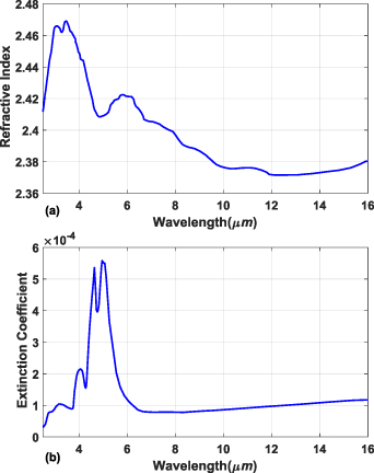
Figure 1. The refractive index (a) and extinction coefficient (b) of polycrystalline diamond across the near and mid-IR (from [10]).
Download figure:
Standard image High-resolution imageUsing current technologies diamond can be readily grown using chemical vapour deposition (CVD) techniques, with qualities matching those of the natural gemstone. In particular, impressive wafer-scale single crystal diamond (SCD) growth using heteroepitaxy of diamond on iridium substrates has been demonstrated for thick films (tens of microns and above) [12], which may eventually offer a viable route to mass production of thin film SCD using layer detachment and transfer techniques. In addition, several fabrication routes for realising nanophotonic structures in bulk SCD have been developed, including bonding and plasma thinning of SCD [13], carving out waveguide structures from bulk SCD [14] and layer isolation using ion beam implantation [15]. A comprehensive recent overview of these and other related techniques can be found in [16]. However, despite the considerable progress made on these fronts, direct wafer-scale growth of thin SCD films on standard semiconductor substrates remains a challenge.
An alternative approach is to grow the CVD thin film from NCD seeds that are pre-deposited on the substrate of choice in colloidal form, resulting in a NCD thin film with much of the physical properties of SCD thin films [17]. This method is quite promising in terms of large area fabrication and scalability and results in film thicknesses in the required range for optical waveguiding. However, the surface roughness of the films can lead to large optical scattering losses at shorter infrared wavelengths [9, 18, 19]. To some extent this can be alleviated through suitable polishing techniques [17, 20]. However, as we will demonstrate here, the film roughness is likely to have less impact on optical losses at longer wavelengths, thus adding to the viability of NCD as a material platform for mid-IR integrated photonics.
As mentioned above, to avoid substrate cladding losses the waveguides should be suspended in air. The geometry of a suspended diamond ridge waveguide is schematically shown in figure 2. This follows our previously demonstrated work on suspended diamond waveguides [9]. There we first created the waveguide ridge by partially etching the patterned diamond film using oxygen reactive ion etching (RIE). This was followed by fully etching the undercut etch holes in a second oxygen RIE step. Finally, the undercut was created through isotropic inductively-coupled RIE of the silicon substrate using SF6 plasma. Details of the film growth and device fabrication can be found in [9, 17]. We will use this architecture as a basis for the designs presented in this work.

Figure 2. Schematic model of the suspended diamond ridge waveguide: (a) 3D view and (b) cross-section.
Download figure:
Standard image High-resolution image3. Design methodology
In the design phase we first find the correct parameters for single mode quasi-Transverse Electric (TE) operation of the suspended ridge waveguides at the wavelengths of interest, using a finite element solver (COMSOL). This involves choosing the correct combination of initial film thickness Hf , ridge height Hr and the width of the waveguide ridge Wr at each wavelength.
The film and membrane thicknesses in these designs are practically constrained by the growth process, mechanical stability, fabrication limitations and the required optical confinement. Due to the wide spectral design range (2.5–16 µm), three different film thickness for different overlapping ranges were assumed: 520 nm for wavelengths between 2.5 and 5 µm, 1000 nm for wavelengths between 4 and 9 µm and 2000 nm for wavelengths between 8 and 16 µm. The choice of 520 nm for the shorter wavelengths is to preserve comparative continuity with our previous work [9]. Growth of thin film NCD with thicknesses of more than a few microns and low top surface roughness is challenging, so we limited our maximum film thickness to 2000 nm. The upper limit of the supporting membrane thickness is governed by optical confinement requirements. A thick membrane will provide less lateral confinement, resulting in higher bending losses and a more spread-out mode. The latter would also require placement of the etch holes at a further distance, resulting in a larger undercut void. On the other hand, a very thin membrane will not be structurally stable. Since we have experimentally demonstrated a structurally stable 170 nm NCD membrane in our previous work [9] we chose this value for the membrane thickness in all cases. Since the film thicknesses are assumed to be three discrete values and in each case the etch depth is fixed by the membrane thickness, the only parameter that can be varied freely is the width of the waveguide, so at each wavelength we find the maximum ridge width for single mode operation. In addition to the constraints on the core and membrane, the etched void under the waveguide ridge should be large enough to minimize optical leakage into the silicon substrate. Finally, the undercut etch holes should be placed sufficiently far away from the waveguide core to avoid optical scattering from the holes. To satisfy these requirements we found the minimum distances for hole placement (Dhole ) and etch depth (Dundercut ) by considering a threshold of 10−12 power drop in the vertical and horizontal directions, respectively. For comparison, this level of isolation lies between that of a 220 nm Silicon-on-Insulator (SOI)-based single mode silicon waveguide with 2 and 3 µm buried oxide layers, operating at 1550 nm (which is the usual standard for telecommunications band silicon photonics).
After choosing the correct set of widths for single mode operation we then calculate the propagation loss of the suspended waveguides by considering the material loss of diamond at the corresponding wavelengths. We also calculate the associated bending losses at these design points using an exact mapping between curvilinear and Cartesian coordinates [21]. Finally, by using a numerical scattering model we estimate the scattering losses for these waveguides across the regions of interest.
4. Design results
4.1. Single mode waveguide dimensions
The suspended rib waveguides were simulated over the 2.5–16 µm range using n and k values reported by Dore [10] for polycrystalline diamond (figure 1). We divided the spectral range into three overlapping sub-ranges based on the assumed film thicknesses of 520, 1000 and 2000 nm, as described in the previous section. The effective index for varying ridge widths at different wavelengths is shown in figure 3. As can be seen, in each sub-range the effective index has reasonably high values, thus ensuring sufficient field confinement and low bending losses. The dark dots indicate the maximum widths for single mode operation at each wavelength (the widths where the next mode starts to appear). These widths are listed in table 1. Note that the listed widths are the upper bounds for single mode operation and in practice should be rounded down appropriately to accommodate fabrication tolerances.
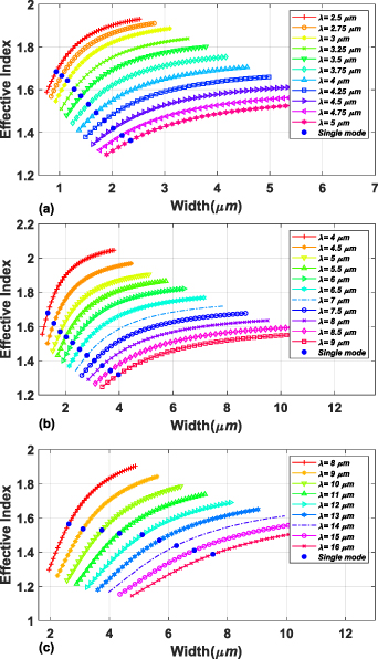
Figure 3. The effective index of the fundamental quasi-TE mode for different waveguide widths in wavelength ranges of: (a) 2.5–5 µm (520 nm film), (b) 4–9 µm (1000 nm film), (c) 8–16 µm (2000 nm film). The dots indicate the design points for single mode operation at each wavelength (exact values listed in table 1) (Note: the plotted wavelengths in (b) and (c) are a subset of the entries listed in table 1).
Download figure:
Standard image High-resolution imageTable 1. Single mode ridge waveguide widths for different film thicknesses and target wavelengths.
| Thickness = 520 (nm) | Thickness = 1000 (nm) | Thickness = 2000 (nm) | ||||||
|---|---|---|---|---|---|---|---|---|
| λ(µm) | nEff | Width (µm) | λ(µm) | nEff | Width (µm) | λ(µm) | nEff | Width (µm) |
| 2.50 | 1.684 | 0.937 | 4.00 | 1.678 | 1.343 | 8.00 | 1.565 | 2.627 |
| 2.75 | 1.665 | 1.041 | 4.25 | 1.650 | 1.452 | 8.50 | 1.558 | 2.899 |
| 3.00 | 1.643 | 1.150 | 4.50 | 1.619 | 1.571 | 9.00 | 1.536 | 3.109 |
| 3.25 | 1.602 | 1.279 | 4.75 | 1.590 | 1.691 | 9.50 | 1.535 | 3.431 |
| 3.50 | 1.571 | 1.406 | 5.00 | 1.570 | 1.804 | 10.00 | 1.529 | 3.748 |
| 3.75 | 1.531 | 1.548 | 5.25 | 1.553 | 1.916 | 10.50 | 1.509 | 3.982 |
| 4.00 | 1.492 | 1.698 | 5.50 | 1.539 | 2.026 | 11.00 | 1.510 | 4.342 |
| 4.25 | 1.456 | 1.853 | 5.75 | 1.523 | 2.142 | 11.50 | 1.509 | 4.731 |
| 4.50 | 1.419 | 2.020 | 6.00 | 1.505 | 2.265 | 12.00 | 1.502 | 5.114 |
| 4.75 | 1.386 | 2.189 | 6.25 | 1.487 | 2.391 | 12.50 | 1.484 | 5.386 |
| 5.00 | 1.362 | 2.350 | 6.50 | 1.467 | 2.527 | 13.00 | 1.469 | 5.694 |
| 6.75 | 1.447 | 2.665 | 13.50 | 1.453 | 5.980 | |||
| 7.00 | 1.431 | 2.799 | 14.00 | 1.438 | 6.272 | |||
| 7.25 | 1.416 | 2.935 | 14.50 | 1.424 | 6.571 | |||
| 7.50 | 1.401 | 3.075 | 15.00 | 1.410 | 6.876 | |||
| 7.75 | 1.386 | 3.218 | 15.50 | 1.397 | 7.172 | |||
| 8.00 | 1.371 | 3.364 | 16.00 | 1.388 | 7.509 | |||
| 8.25 | 1.356 | 3.517 | ||||||
| 8.50 | 1.342 | 3.668 | ||||||
| 8.75 | 1.330 | 3.818 | ||||||
| 9.00 | 1.318 | 3.971 | ||||||
The waveguide losses at each of the single mode points are calculated using the corresponding width and bulk diamond absorption (figure 4). As figures 4(b) and (c) indicate, the waveguide losses above 6 µm are less than 10 dB cm−1, indicating that waveguide operation at these wavelengths is feasible. In the range of 2.5–6 µm the material and multiphonon-induced absorption result in high waveguide losses, especially in the 4.5–5 µm band. However, diamond waveguides may still be operable in this part of the spectrum despite this loss. This is particularly true for the thinnest (520 nm) film, where a large proportion of the mode resides in the air cladding and the highest losses remain below 50 dB cm−1 (figure 4(a)). While this level of loss will not be practical for centimetre-scale and longer waveguides, it may still be possible to operate millimetre scale devices in this wavelength range.

Figure 4. Single mode waveguide material losses for different wavelength ranges and the widths specified in table 1: (a) 2.5–5 µm (520 nm film), (b) 4–9 µm (1000 nm film), (c) 8–16 µm (2000 nm film). The waveguide loss above 6 µm is below 10 dB cm−1 and decreases uniformly, indicating the usability of this region for integrated photonics applications (note: The single mode waveguide widths used for calculating the losses between the listed wavelengths were found by linear interpolation of the widths of waveguides at the adjacent design points).
Download figure:
Standard image High-resolution image4.2. Bending losses
Having calculated the widths for single mode operation we then calculate the bending losses for different bend radii at each wavelength and corresponding width. Owing to the nature of the suspended rib waveguide, most of the radiative losses associated with bending are due to leakage into the slab modes of the supporting membrane. The bend losses were calculated by using an exact equivalent straight waveguide model [21] which yields accurate results without incurring any approximations.
As expected, the bend losses for a fixed bend radius increase with wavelength. However, even in the 16 µm wavelength limit it is possible to achieve less than 0.1 dB per 90 degree bend with bend radii less than 100 µm using a 2000 nm thick diamond film. At the other end of the spectrum (2.5 µm) this is achievable with bend radii as small as 23 µm (figure 5).
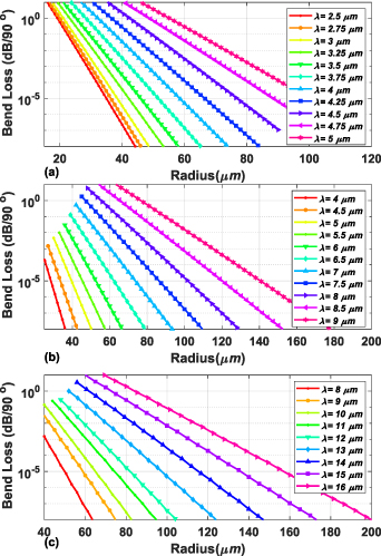
Figure 5. Bend losses vs. bend radius for the waveguides fabricated from different film thicknesses: (a) 520 nm, (b) 1000 nm and (c) 2000 nm. The waveguide widths corresponding to each wavelength are listed in table 1.
Download figure:
Standard image High-resolution image4.3. Hole placement and undercut depth
As discussed above, the placement of the holes and the extent of lateral and vertical undercut is important for correct operation of the waveguide platform. The high refractive index of silicon will induce substrate leakage if the undercut is too small. Likewise, the large index difference between diamond and air will enable the etch holes to act as highly efficient scatterers, thus inducing additional losses. In some situations, this may even lead to Bragg contra-directional scattering due to the periodicity of the holes. To avoid these issues, the lateral distance between the waveguide core and the holes and the vertical distance between the core and the silicon substrate should be sufficiently large to avoid any disturbance of the optical mode. The need for isolating the waveguide mode is not unique to our suspended waveguide architecture and occurs in other waveguide platforms. In particular this also needs to be considered in the SOI platform, where the buried oxide layer has to be thick enough to avoid leakage of the mode power into the high index silicon handle. Therefore in our design we use the structural specifications of experimentally demonstrated single mode SOI waveguides as a guideline. Assuming an operating wavelength of 1550 nm, a single mode silicon waveguide with width and height of 400 nm × 220 nm and a buried oxide layer of 2 µm (which is a common specification for single mode waveguides in SOI), the drop in power at the handle/oxide interface is calculated to be slightly larger than 10−12. Using this experimentally validated power drop for isolation we obtain the minimum undercut and hole distance by calculating the 10−12 power drop points in the lateral and vertical directions. figure 6 shows the required horizontal hole placement for the full range of 2.5–16 µm. Following the previous approach and results, this range is also divided into three regions, based on the targeted film thicknesses. The distance Dhole is measured from the inner edge of the etch hole to the centre of the waveguide ridge.

Figure 6. The minimum required distance for hole placement at wavelength ranges: 2.5–5 µm (520 nm film), 4–9 µm (1000 nm film) and 8–16 µm (2000 nm film).
Download figure:
Standard image High-resolution imageSimilarly figure 7 shows the required vertical etch depth for different wavelengths in the regions corresponding to the three film thicknesses, using the same 10−12 power drop metric. It is of interest to note that the required vertical etch depth is slightly less than the lateral etch in all cases, partly since the presence of the diamond membrane contributes to relatively larger horizontal leakage of the mode. For a wavelength of 2.5 µm and a 520 nm film the minimum undercut etch is just below 6 µm while at the other end of the spectrum an etch undercut of at least 36 µm is needed for a waveguide fabricated from 2000 µm operating at 16 µm. These results indicate that even the largest undercuts can be reliably fabricated using an isotropic silicon etch process (for example XeF2 [22] or purely inductively coupled SF6 plasma [23, 24] silicon isotropic etching). Such undercuts can also be created using wet isotropic silicon etchants such as HNA (HF:HNO3:C2H4O2) [25] or solvent-modified TMAH [26], however care must be taken to avoid surface tension damage during the drying process, especially for the larger undercuts.
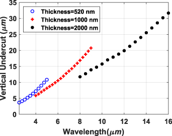
Figure 7. The minimum required vertical undercut at wavelength ranges: 2.5–5 µm (520 nm film), 4–9 µm (1000 nm film) and 8–16 µm (2000 nm film).
Download figure:
Standard image High-resolution imageFinally, the modal distributions (electric field norm) of a subset of the waveguides at their corresponding wavelengths are depicted in figure 8. All cases indicate good lateral and vertical mode confinement.

Figure 8. Quasi-TE eigenmodes (electric field norm) for various design points: λ0 = 2.5 µm with width = 937 nm (520 nm film), (b) λ0 = 5 µm with width = 1005 nm (520 nm film), (c) λ0 = 4 µm with width = 1343 nm (1000 nm film), (d) λ0 = 9 µm with width = 3971 nm (1000 nm film), (e) λ0 = 8 µm with width = 2627 nm (2000 nm film), (f) λ0 = 16 µm with width = 7509 nm (2000 nm film). Each sub-figure scale is adjusted to its corresponding waveguide dimensions.
Download figure:
Standard image High-resolution image4.4. Estimation of membrane sag
Since the suspended membrane is thin (170 nm) and the lateral etch can be on the order of tens of microns, the question of the mechanical stability of such a structure may arise. To address this we consider the extreme case of the largest hole position (35.7 µm) and the widest and tallest ridge (width of 7.509 µm and height of 1830 nm, corresponding to the waveguide design for 16 µm operation). Assuming that the holes are placed symmetrically on both sides of the core and an isotropic etch process is used for creating the undercut, the overall width of the suspended membrane (Wm ) will be approximately four times the hole distance (142.8 µm). Using this data, we can estimate the overall membrane sag by considering the individual contributions from the weight of the waveguide ridge Sr (modelled as a point load) and the sag due to the weight of the membrane itself Sm (modelled as a distributed load). To a first approximation the structure can be analysed with a 2D cross section by disregarding the presence of the etch holes (which is a valid approximation if the holes have small diameters (in practice less than 5 µm) and are not closely spaced). Following this, in each load case the membrane sag is calculated using the Euler-Bernoulli beam deflection formulas for simply supported beams under point and distributed loads [27, 28]:
where E and ρ are the Young's modulus (1050 GPa) and density (3515 kg m−3) of diamond, respectively and g is gravitational acceleration (9.8 m s−2). From these, the membrane sags due to the point and distributed load contributions are calculated to be 17 and 15 pm respectively. Since the displacements are very small the overall sag can be calculated as the sum of these contributions (since a linear approximation is valid here), giving a total sag of 32 pm which is quite negligible compared to the membrane and undercut lengths. This provides reassurance regarding the mechanical stability of the suspended waveguides. This prediction is also supported by the SEM image in figure 9, which shows a suspended undercut NCD film of 170 nm thickness (fabricated as part of the work flow described in [9]) using isotropic SF6 plasma etching. The varying width of the undercut is due to the additional etching pathway from the exposed edge of the chip, in addition to the etch holes. This clearly shows that mechanically stable membranes of NCD with large undercuts can be readily fabricated. It is also of interest to note the absence of any apparent stress-induced ripples in the membrane. The 175 µm undercut shown in the image is far in excess of the required 142.8 µm undercut needed for 16 µm operation.
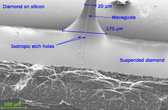
Figure 9. Nanocrystalline suspended ridge waveguide fabricated from a 520 nm diamond film grown on silicon. The thinned membrane thickness is 170 nm and the undercut was created by isotropic etching of silicon using SF6 inductively coupled plasma etching.
Download figure:
Standard image High-resolution image5. Estimation of scattering losses
In addition to the material and bending losses covered in the previous sections, another major source of losses in NCD waveguides is due to scattering from the uneven top surface of the film, which can dominate other losses [9]. This is in contrast to SCD, which has a much smoother surface (but is not easily adapted to wafer-scale thin film growth, as described in the introduction). The roughness is inherent to the NCD film growth process and becomes more pronounced with increasing film thickness [17]. While polishing processes can reduce the roughness, it is unlikely that the film smoothness will approach the quality of other standard semiconductor platforms (such as CMP polished crystalline silicon), given that the film is grown from randomly scattered diamond seeds, which are also random in size and shape themselves. Given this, it is important to estimate the expected scattering losses in NCD waveguides, which will be a deciding factor in the practicality of NCD integrated photonics. Note that since the bottom surface of the NCD film is usually adjacent to and bounded by a smooth polished substrate (e.g. silicon), the dominant scattering loss is expected to be mainly due to the top surface roughness. Likewise, the losses due to the etched sidewall roughness are expected to be negligible compared to the top surface roughness losses, since they originate from the mask roughness, rather than the polycrystalline composition of the diamond film. This is in contrast to SOI waveguides, where the polished top surface has sub-nanometre roughness features and so sidewall roughness becomes a dominant loss mechanism.
Intuitively one would expect that as the wavelength increases the scattering losses should decrease, owing to the reduction of the ratio of roughness features to wavelength. To quantitatively investigate and estimate these losses we use the Payne-Lacey model [29], which offers a reasonable estimate for scattering losses in a slab waveguide with a prescribed thickness d, core/cladding refractive index (n1 and n2) and roughness statistics (i.e. RMS roughness σ and autocorrelation length Lc ). For a slab mode with free space wavevector k0 and effective index neff , the loss coefficient is given as [29]:
where
and
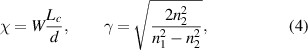
The additional factor of 1/2 in equation (3) for α, compared to the original Payne-Lacey formula [29], reflects the assumption that only the top surface roughness of the slab is considered here. Figure 10(a) shows the calculated effective index for the first TE slab mode across the full spectrum of interest for each of the three film thicknesses. For each thickness the spectral range is chosen to follow the parameters of our simulations in the previous sections (e.g. 520 nm for the range 2.5–5 µm, etc). In practice the surface roughness of NCD can vary a great deal depending on the growth conditions and film thickness. Unpolished roughness values below 20 nm have been reported by different groups [17, 30], while polishing techniques can reduce this to below 5 nm [17]. Likewise, autocorrelation lengths varying from a few tens to a few hundreds of nanometres have been reported [9, 30]. For our simulations we conservatively assumed two surface roughness values of 15 nm and 30 nm (corresponding to slightly polished and unpolished films, respectively) and a representative autocorrelation length of 100 nm. Applying these to the Payne-Lacey formulas the scattering losses can then be estimated (figure 10(b)). For comparison, the material losses of the first TE mode for the three slab thicknesses in these spectral ranges are also plotted. Note that the scattering losses drop noticeably as the film thickness is increased, which is due to reduced optical intensity of the first TE mode on the film-air boundary as the slab thickness is increased. More importantly, in all cases the results show a drastic reduction in the waveguide losses as the wavelength is increased (about a factor of 700 reduction in dB cm−1 at 16 µm compared to 2.5 µm for all values of σ considered here). In particular, at wavelengths larger than 7 µm the estimated scattering losses become progressively lower than the material losses. While this simple model does not capture all of the possible scattering losses (e.g. sidewall roughness scattering resulting from plasma etching) it does provide a promising outlook for the practicality of suspended NCD as a mid-IR integrated photonics platform.
Figure 10. (a) The effective index of the first TE mode for suspended diamond slab waveguides with various thicknesses. (b) Waveguide scattering losses for varying RMS values of surface roughness. The slab thicknesses and corresponding spectral ranges were chosen to follow the same thickness assumptions in the waveguide design process. The resultant 3-part segmented loss curves correspond to the losses in each slab waveguide (520, 1000 and 2000 nm slab waveguides from left to right, respectively). The losses curves are discontinuous due to the different spatial distribution of the modes corresponding to each slab thickness.
Download figure:
Standard image High-resolution image
6. Conclusion
Designs have been presented for single mode suspended ridge waveguides operating in a wide range of wavelengths covering 2.5–16 µm. In all cases the waveguides exhibit good optical confinement, resulting in small bend losses with reasonably small bend radii. As expected, the wide optical transparency spectrum of diamond results in acceptable material losses in the suspended waveguides for wavelengths larger than 6 µm. Also, despite the relatively strong absorption of diamond below 6 µm the waveguides can potentially be of practical utility if the overall device lengths are limited to 1 mm or less. The undercut depths required for optical isolation are also reasonably small (i.e. the largest undercut membrane (for 16 µm operation) has a total width of less than 150 µm), resulting in mechanically robust suspended structures that are compatible with standard microfabrication techniques. While the inherent surface roughness of NCD will inevitably contribute to waveguide scattering losses, these are predicted to become negligible as the wavelength of operation is increased. These results present a promising outlook for the development of mid-infrared integrated photonic devices and systems using NCD thin films grown on standard semiconductor substrates.
Data availability statement
The data that support the findings of this study are available upon reasonable request from the authors.
Acknowledgments
This work was supported by the EPSRC Future Photonics Hub Innovation Partnership Fund (Grant No. EP/N00762X/1) and EPSRC/UKRI Innovation Fellowship (Grant No. EP/S001425/1). Helpful discussions with Prof. Oliver A Willams and Dr Soumen Mandal at Cardiff University regarding the growth of nanocrystalline diamond thin films and their properties are acknowledged.