
Abstract
The depinning field (HD) of vortex domain walls in a permalloy wire with an asymmetric triangle notch was investigated through magneto-optic Kerr effect (MOKE) microscopy and micromagnetic simulations. Wires of various widths with notches fixed on the wall's incoming side angle were studied for various outgoing side angles (ϕ). The curves of HD of wall versus ϕ were measured by MOKE microscopy. Micromagnetic simulations were used to obtain curves of the HD of the wall versus ϕ. The maximum of such a curve of tail-to-tail -clockwise wall is known as the transition angle (ϕT). The shape-anisotropic energy (EA) of the notch outgoing side wire and the exchange energy (EEx) of the wall–notch interaction competed to influence the ϕT value. Pinning potential was increased by the EEx when ϕ was smaller than the ϕT. Pinning potential was considerably reduced by the small EA when ϕ was larger than the ϕT. Furthermore, the ϕT value changed with the decrease in the depth of the notch because EA was influenced by notch depth.
Export citation and abstract BibTeX RIS

Original content from this work may be used under the terms of the Creative Commons Attribution 4.0 licence. Any further distribution of this work must maintain attribution to the author(s) and the title of the work, journal citation and DOI.
1. Introduction
Magnetic-domain-wall-based devices, such as shift register [1], vortex domain wall trajectory [2, 3], magnetic logic devices [4–7], and the time-delay oscillator [8], have attracted considerable attention. Precise control of the wall position, stable wall structure, and adjustment of wall chiralities are critical in such applications. Creating a pinning site is a method to stabilize wall structures and control wall positions. Pinning sites are of two types, namely nongeometric and geometric. Nongeometric pinning sites are formed through a local change of magnetic properties and annealing-induced local diffusion from the nonmagnetic metal into the magnetic wire [9, 10]. Another method to generate a pinning site is through exchange bias [11, 12], which is produced from crossed ferromagnetic wires and antiferromagnetic bars [11]. In geometric pinning sites, single-notch, double-notch, antinotch, protrusion and stepped-wire methods can be used to pin the wall [6, 8, 9, 13–27]. Numerous factors, such as wall chirality, the width of magnetic wires, the thickness of magnetic wires, and the depth of notches, influence the interaction between the notch and the wall [9, 13–15, 18–20, 27] and the wall pinning potential. The competition between exchange interaction and anisotropies (e.g., crystalline anisotropy or shape-anisotropy) affect domain wall's spatial profile [8]. Domain wall length and structure are affected by the crystalline anisotropy and the magnetic exchange interaction [24]. Studies have reported the depinning field (HD) for wires with a notch [9, 13–19, 25–29]. The walls in wide wires exhibit a lower wall energy per unit cross-sectional area. Furthermore, the HD values in wide wires are smaller than those in narrow wires [15]. The HD values for in-plane anisotropic wires were influenced by the potential energy of side wells (EW) and potential energy of center barriers (EB) in the pinning potential landscape [9, 14, 15]. The HD provides the wall energy to overcome the EW or EB for artificial pinning sites, such as in the notches. A shallow EW or small EB results in a low HD requirement for wire depinning from the notch [15]. The wall structures of the wires of various widths differs considerably [30]. Thick and wide wires exhibit a multi-vortex wall structure [30, 31]. However, the depinning behaviors of a wall for a wire with different symmetries of triangular notch differs considerably. As displayed in figure 1, the incoming angle (θ) is the angle between the long axis of the wire and the wall injection direction side of an asymmetric triangular notch, and the outgoing angle (ϕ) is the angle between the long axis of the wire and the wall lifting side of the asymmetric triangular notch [19]. In 2014, Brandão et al observed vortex domain wall pinning and depinning in submicron wires with an asymmetric notch with fixed θ values and various ϕ values; they revealed that HD increased with increasing ϕ values [19]. The depinning behavior is also influenced by the shape-anisotropic energy (EA) of the outgoing side wire [9]. Here, EA influences EB and the pinning potential landscape. However, few studies have discussed the influence of wall depinning behavior and physics on the various ϕ values of a notch. To understand in-plane anisotropic wall dynamics, we focused on the wall depinning behavior in a wire with an asymmetric notch.
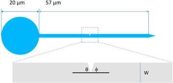
Figure 1. Setup of the experiment devices. Enlarged image of the notch with a triangular notch at the bottom, where θ, ϕ, and W are the incoming, outgoing angles, and wire width respectively.
Download figure:
Standard image High-resolution image2. Experiment and simulation
We designed samples of wires with various widths and an asymmetric notch, as displayed in figure 1. A 20 μm in diameter circular pad was connected with a 20 nm-thick straight magnetic wires of widths 1 and 2 μm and length of 57 μm. To eliminate the edge domain and the formation of the wall, the wire was tapered at its ends [16, 19]. The asymmetric triangular notch had a fixed notch depth ratio (notch depth divided by wire width, Rd), fixed incoming angle (θ), and various outgoing angles (ϕ). In this study, θ = 60° and ϕ was varied by 15° from 15° to 60° to determine the relationship between HD and ϕ. To transfer the designed sample patterns onto Si wafers, we used e-beam lithography and the lift-off process. Next, we deposited a 20 nm-thick permalloy (Py) films onto the layer of pattern transferred poly(methyl methacrylate) Si wafers through DC magneto sputtering at a background pressure of 1 × 10⁻⁷ Torr. A magneto-optical Kerr effect (MOKE) microscope was then used to capture magnetic domain images and determine the depinning field (HD) values. We used the GPU-accelerated micromagnetic simulation software Mumax3, which is based on the Landau–Lifshitz equation [32]. We eliminated magnetic charges on the left and right ends of magnetic wires to create an infinitely long wire system [30, 31] and set the wire length L ≥ 8 times the wire width. Furthermore, most of our simulations were performed at a zero temperature. We used the energy minimization function to set the wall structure and then performed the field-driven wall depinning simulation in wires of various widths [30–33]. To examine to influences of thermal fluctuation and surface defects, we run the simulation with surface defects at 300 K. The surface defects were set by GrainRoughness function of Mumax3. The GrainRoughness parameters of grain size, minimal height and maximal height are 5 nm, 0 nm, and 5 nm, respectively and the random seed of the GrainRoughness are 2997, 2998 and 3000. Py was used as the simulation material of all wires; the saturation magnetization (Ms), exchange stiffness (Aex), magnetic crystalline anisotropic energy constant, and damping constant were 860 emu cm−3, 1.3 × 10⁻⁶ erg cm−1, 0 erg cm−1, and 0.01, respectively. To swiftly simulate our vortex domain wall depinning behavior, we ran the simulation at cell sizes of 5 nm × 5 nm × 5 nm or 5 nm × 5 nm × 20 nm.
3. Results and discussion
One of the domain and depinning images of the MOKE microscope for a 2 μm-wide wire with an asymmetric triangular notch are displayed in figure 2. The θ and ϕ values of the notch of the wire were 60° and 30°, respectively. Figure 2(a) displays the images of the injection field and HD of the tail-to-tail-type clockwise (TT-CW) wall, which had values of −5.18 and −19.94 Oe, respectively. The injection field and the HD of the tail-to-tail-type counterclockwise (TT-CCW) wall were −5.38 and −11.94 Oe, respectively, as displayed in figure 2(b). The head-to-head-type counterclockwise (HH-CCW) wall and the TT-CW wall exhibited the same symmetry of wall configuration and the same interaction between the domain wall and the notch. Therefore, their HD values were almost the same. Similarly, the HD values of the TT-CCW and HH-CW walls were identical [19]. This study focused on the TT-type domain walls. Figure 3 depicts HD as a function of ϕ for the TT-walls for 1- and 2 μm-wide wires. HD value of TT-walls was negative because the applied field was toward to left. Here, we defined HD value as positive value. The maximum HD values of the TT-CW wall in these wires were approximately 17.48 and 19.64 Oe, respectively, at ϕ = 30°. The HD of the TT-CCW wall was lower than that of the TT-CW wall, as displayed in figures 3(a) and (b). To understand the wall depinning behavior, we simulated the vortex wall propagation for wires with an asymmetric notch. The micromagnetic simulation revealed that the depinning behaviors of the HH-CCW and TT-CW walls in the 1 μm-wide wire were the same, as displayed in figure 3(c). This behavior was consistent with the experimental results. The maximum HD value of the TT-CW and HH-CCW walls in the simulated HD–ϕ curves were approximately 74 Oe in the 1 μm-wide wire at ϕ = 35°, as displayed in figure 3(c). The simulated results were consistent with the experimental depinning behaviors and exhibited the same trend for the HD–ϕ curves. The ϕ value of the maximum HD is defined as the transition angle (ϕT). The quantitative differences in HD between the experimental and simulation results were caused by the thermal fluctuation and sample defects. To confirm the room-temperature and surface defects influences, we ran simulations of the 1000 nm-wide wire with surface defects at 300 K, as shown in figure 3(d). We chose the ϕ equal to 30°, 35°, and 40° to run the simulations. Blue line of figure 3(d) displayed averaged HD values that were calculated by the wires with different random seeds of GrainRoughness function. The averaged HD values with surface defects at 300 K are around 47, 56.2, and 46.7 Oe at ϕ equal to 30°, 35°, and 40°, respectively. Figure 3(d) revealed that room-temperature and surface defects reduced HD values, but unobviously affected ϕT value. We utilized EdgeSmooth function of Mumax3 to observe straircase effect for the notch. The simulated results with EdgeSmooth function are similar to those without EdgeSmooth function. It indicates that the straircase effect of asymmetric notches has a weak influence on our study.
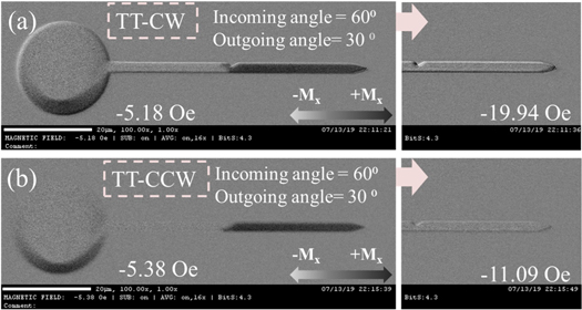
Figure 2. Magnetic optic Kerr effect microscopy images for a 2 μm-wide wire with a asymmetric triangular notch. The notch has a 60° incoming angle and a 30° outgoing angle. (a) Tail-to-tail (TT)-clockwise (CW) wall pinning and depinning. (b) TT-counterclockwise (CCW) domain wall pinning and depinning. Color map shows the direction of magnetization in the magnetic images.
Download figure:
Standard image High-resolution image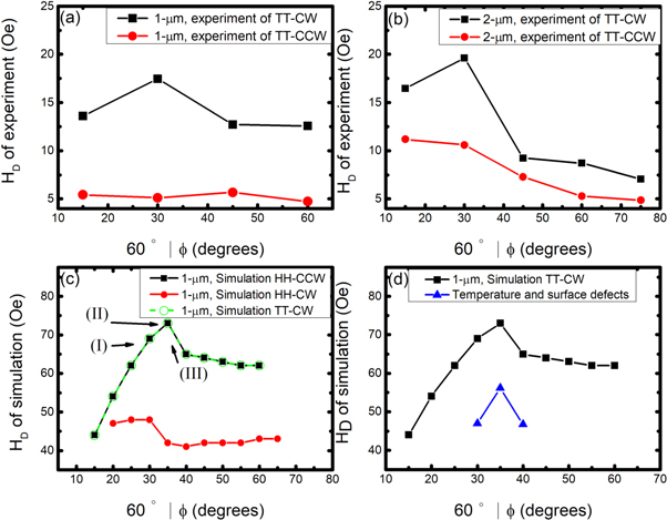
Figure 3. (a) and (b) Depinning field (HD)–outgoing angle (ϕ) curves of tail-to-tail-vortex wall in 1- and 2 μm-wide wires. The black and red lines represent the tail-to-tail (TT)-clockwise (CW) and TT- counterclockwise (CCW) walls, respectively. (c) Simulation of the HD-ϕ curves of head-to-head (HH)-CCW, HH-CW, and TT-CW walls. The black solid square, red solid circle, and green open circle represent the simulated HH-CCW, HH-CW, and TT-CW walls, respectively. Roman numerals in (c) mark the time evolution of the simulation, as displayed in figure 4. (d) Simulation of the HD-ϕ curves of TT-CW walls in the 1 μm-wide wire. The black line represents the simulation without surface defects at 0 K. The blue line represents the averaged HD with surfaced defects at 0 K. X-axis label of 60°∣ ϕ (degrees) means the notch has a fixed incoming angle of 60° and various ϕ.
Download figure:
Standard image High-resolution imageIn order to examine the depinning process, we saved the Mumax3 output of the TT-CW wall parameter in the 1 μm-wide wire before the depinning state at the near HD and performed the time evolution simulations at the HD. Figure 4 displays the simulated TT-CW wall depinning process for the wires with notches of ϕ = 30°, 35°, and 40°, respectively, as displayed in figure 3(c). The top of figure 4 displays the state of the wall near HD values before depinning and the state of the wall with applied fields of −68, −72, and −64 Oe for ϕ values of 30°, 35°, and 40°, respectively. When the wall approached the notch, the applied field compressed the wall at the incoming side of notch, as displayed at the top of figure 4. During the depinning process, when the wall arrived at the notch, a boundary line that was leaning to the right appeared at the right of the wall, as denoted by the black arrow in figure 4(a). Because the wall was compressed, the boundary line of the wall became an arc at the notch sharp to easily pass through the notch and go to the outgoing side of the notch with ϕ = 30° or 35°. A new domain (green color) gradually formed from 0 to 4.6 ns in the outgoing side, as displayed in figures 4(a) and (b), and then the wall was depinned from the notch. The simulated depinning images are displayed in figure 4 at 19.8 ns. However, the time evolutions for the wire with ϕ = 40° in figure 4(c) differed from those for the wires with ϕ = 30° and 35°, as displayed in figures 4(a) and (b). The wall depinning process shown in figure 4(c) revealed that the new domain was generated on the outgoing side of the notch at an applied field of −64 Oe.

Figure 4. Time evolution simulations of tail-to-tail clockwise wall depinning in 1 μm-wide wires with an asymmetric notch. Notches have a various outgoing angles (ϕ) and fixed incoming angle (θ). We denoted the θ and ϕ of notch as θ∣ ϕ. These simulation wires has fixed θ value equal to 60°. (a), (b), and (c) correspond to those in figure 3. (I), (II), and (III) are notches with 30°, 35°, and 40° of ϕ values, respectively. Gray triangle arrows display the direction of the simulated magnetic domain in simulated wires.
Download figure:
Standard image High-resolution imageThe wall depinning behavior is related to the wall pinning potential energy landscape [9, 15, 28]. As indicated in [9], the wall pinning potential well or barrier is generated by the asymmetric notch. Both the shape of the notch and the wire width influence the wall depinning behavior. Therefore, the depinning behaviors in figure 4 are influenced by the potential energy of the side well (EW) at the incoming side of the notch and the pinning potential energy barrier (EB) at the outgoing side of notch. For notches with the same depth and θ, the EW values are almost the same [9]. Therefore, the influence of EW on the depinning behavior can be ignored, and the EB dominates the HD. The EB value is composed of the local exchange energy (EEx) and EA. EEx denotes the exchange energy between the right side of the wall and the magnetic moments located at the outgoing side region of the notch, and EA indicates the shape-anisotropic energy of the outgoing side wire. EEx is affected by the dot product between right side the wall and magnetic moments located at the outgoing side region. Direction of moments located at outgoing side region is aligned along outgoing side. Therefore, EEx increased with ϕ increased. The various ϕ changed both EA and EEx. Thus, EB can affect the depinning behavior. During the depinning process of the wall, the applied field caused the wall to overcome the notch pinning. The wires with higher ϕ values exhibited larger EEx values because of the greater interaction between the right side of the wall and the magnetic moments located at the outgoing side region of the notch. However, EA became smaller as the ϕ value increased because the local demagnetic energy density increased and a new wall was created from the outgoing side region of the notch, which facilitated depinning. EA and EEx competed for the influence on depinning. When the ϕ was smaller than ϕT, EEx increased with increases in ϕ, but EA slowly decreased at the same time. These results increased EB, which resulted in a higher HD. EA was strongly dependent on ϕ. EA decreased slowly for small angles but decreased rapidly for large angles, with ϕT as the crossover point. As the ϕ was further increased, the influence of EA exceeded that of EEx. EB and HD were considerably reduced by the small EA when ϕ was larger than the ϕT. To reduce the local demagnetic energy density, a vortex wall core and a new wall were created at the outgoing side of the notch, and the HD was then reduced, as displayed in figures 3 and 4(c). We ran the simulation of 400- and 500 nm-wide wires with θ = 45° and 60° to examine the influences of θ. Figure 5 revealed that the incoming side of notch affected EW and HD values, but both ϕT values appeared at ϕ = 35°. It indicates that the incoming side of the notch has less influence on EA and EEx.
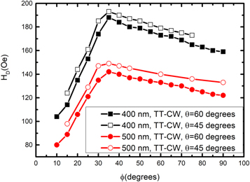
Figure 5. Simulations of depinning field (HD)–outgoing angle (ϕ) curves of tail-to-tail (TT)- clockwise (CW) walls with different incoming angles (θ). Black solid square, red solid circle, and green open circle represent the simulated TT-CW walls in 400- and 500 nm-wide wire with θ = 60°, respectively. Black open symbols and red open symbols displayed simulated TT-CW walls in 400- and 500 nm-wide wire with θ = 45°, respectively.
Download figure:
Standard image High-resolution imageTo confirm the effect of EA, we simulated half wires with a single arm of outgoing side wire. The single-arm wires exhibited a left half wire with a half notch with depth Rd fixed at 50%. Figure 6(a) displays simulations of a single-arm wire. We simulated the single-arm wires without a wall initially, as displayed in figure 6. The simulations revealed a single-arm wire with a reversal field (HR), which caused the single arm to shift from a negative saturation state to a positive saturation state. The HR–ϕ curves were plotted for single-arm wires to compare the simulated HD for whole wires with a notch. Figure 6(b) displays the results of 300-, 400-, and 500 nm-wide single-arm and whole wires. For single-arm wires, the HR value decreased with ϕ. Furthermore, the HR values of single-arm wires differed considerably from those of the whole wires. However, the decreasing trends of HD and HR were quite similar between ϕ values of 35° and 90° for all simulated wires. The shape of the single-arm wire was the same as the right side of the whole wires but differed on the left side. The reversal of the magnetic saturation state depended on EA for the single-arm wires. For the single-arm wire, magnetic switching behavior was only affected by outgoing side of notch. The HR for the single-arm wires only depended on EA and decreased as ϕ increased. These results displayed a same trend when ϕ larger than the ϕT for both single-arm wire and whole wire. It displayed the EA that was dominant in the depinning behavior for ϕ larger than the ϕT. For the whole wire simulation, the wall HD values increased with ϕ increased when the ϕ smaller than ϕT. It indicated that the EEx increased with ϕ increased because EB value was composed of EEx and EA. The HD values were affected by EEx for the range of ϕ to ϕT. As displayed in figure 6(b), the competition between EA and EEx is independent on the wire width.
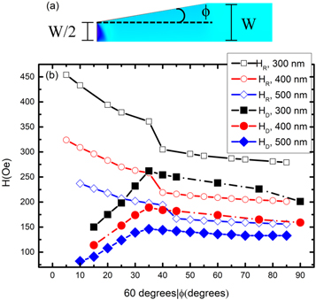
Figure 6. (a) Example of an outgoing side-single-arm simulation. (b) Applied field (H)–outgoing angle (ϕ) curves of the outgoing side-single-arm simulation reversal field (HR) and whole wire simulation depinning field (HD). Open symbols and solid symbols displayed the single-arm simulations and whole wire simulations, respectively. X-axis label of 60 degrees∣ ϕ (degrees) means the notch has a fixed incoming angle of 60 degrees and various ϕ.
Download figure:
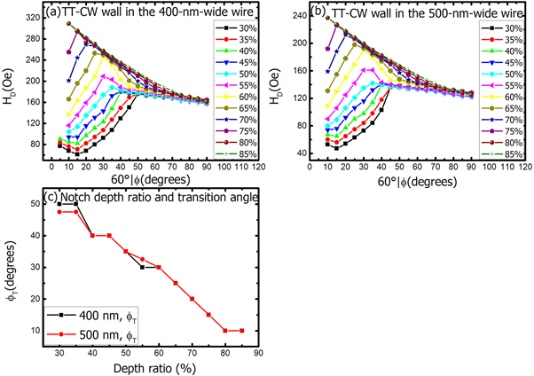
Standard image High-resolution imageMoreover, the Rd of the notch was simulated to confirm the influence of EA and the ϕ. We varied the Rd to adjust the competition between EA and EEx for the 400- and 500 nm-wide wires with asymmetric notches and various Rd values, as displayed in figure 7. In these simulations, the θ of the notch was the same and the ϕ of notch was varied. The ϕT value in the HD–ϕ curves was dependent on the Rd for the wires, as illustrated in figures 7(a) and (b). With the same wire asymmetry, the notch with the larger Rd resulted in a smaller ϕT value. For both 400- and 500 nm-wide wires simulations, the ϕT values for the wires with Rd between 30% to 85% were approximately 50° to 10°, respectively, which revealed that the ϕT value was almost independent on the width of the wires, as illustrated in figure 7(c). Because of anisotropy, the moments on both sides of the notch tend to align the edge of the notch. Deeper notches exhibit higher magnetic moments aligning the sides of the notch. Large Rd values enhanced the energy depth of EW and increased the HD value. The Large Rd changed ϕT value because depth of notch affected the competition between EA and EEx. The notch with a high Rd extended the length of the outgoing side of the notch, which produced a strong influence on EA for the HH-CCW wall depinning. A small EA due to the large Rd leads to the reduced HD value. The anisotropy of notch with high Rd lead the EA was easily to dominate the depinning behavior. Moreover, a high Rd resulted in a large local demagnetic energy density at the outgoing side of the notch. Therefore, a new domain was easily generated at the outgoing side of the notch for reducing the total energy.
Figure 7. (a) and (b) Simulated HD–ϕ curves of the head-to-head-counterclockwise vortex domain wall in 400- and 500 nm-wide wire with various notch depth ratios (notch depth divided by wire width). X-axis label of 60°∣ ϕ (degrees) means the notch has a fixed incoming angle of 60° and various. (c) Curves of transition angle (ϕT) versus notch depth ratio for 400- and 500 nm-wide wires.
Download figure:
Standard image High-resolution image
4. Conclusion
We performed MOKE microscopy and micromagnetic simulations on Py wires with asymmetric triangular notches to investigate the factor influencing the wall depinning behavior. The maximum of the HD–ϕ curves, which is known as the ϕT, is well observed for all wires. The experiments revealed that the ϕT was independent on wire widths. Micromagnetic simulations revealed that the ϕT values in the HD–ϕ curves of the TT-CW and HH-CCW walls for wires with an asymmetric triangular notch were influenced by EA and EEx. Simulations of wires with asymmetric triangular notches revealed the competition between EA and EEx for influencing the curves. The single-arm and various Rd values simulations also revealed the affection of EA for depinning behavior. EEx dominated HD in the HH-CCW and TT-CW walls for ϕ < ϕT, and EA dominated HD for ϕ > ϕT. The simulation of the wall depinning for the notch with various Rd values revealed that the ϕT value decreased as Rd increased and was almost independent of the wire width.
Acknowledgments
This work was supported by Ministry of Science and Technology, Taiwan under Grant Nos. MOST-106-2112-M-018-007 and MOST-107-2112-M-018-004.
Data availability statement
The data generated and/or analysed during the current study are not publicly available for legal/ethical reasons but are available from the corresponding author on reasonable request.