
Abstract
Health monitoring of structures and people requires the integration of sensors and devices on various 3D curvilinear, hierarchically structured, and even dynamically changing surfaces. Therefore, it is highly desirable to explore conformal manufacturing techniques to fabricate and integrate soft deformable devices on complex 3D curvilinear surfaces. Although planar fabrication methods are not directly suitable to manufacture conformal devices on 3D curvilinear surfaces, they can be combined with stretchable structures and the use of transfer printing or assembly methods to enable the device integration on 3D surfaces. Combined with functional nanomaterials, various direct printing and writing methods have also been developed to fabricate conformal electronics on curved surfaces with intimate contact even over a large area. After a brief summary of the recent advancement of the recent conformal manufacturing techniques, we also discuss the challenges and potential opportunities for future development in this burgeoning field of conformal electronics on complex 3D surfaces.
Export citation and abstract BibTeX RIS
1. Introduction
Though most sensors and electronics are fabricated on 2D planar substrates (e.g. silicon wafers [1] or glass plates [2]), the integration of electronic systems on 3D curvilinear surfaces starts to gain momentum in bio-integrated devices [3–6], health monitoring of various structures [7, 8], and 3D multifunctional electronics [9]. In addition to the 3D complex shapes, the soft, hierarchically structured, dynamically changing biological surface [10] presents significant challenges for the device fabrication and integration. Efforts to address these challenges lead to the rapid development of various stretchable structures with advanced fabrication approaches to integrate the devices on the 3D curved surfaces. The exploration of novel nanomaterials and their composites further expands the functionality and capability of the resulting devices. The ever-growing repertoire of these 3D conformal electronics opens up opportunities in 3D antenna and RF devices [9, 11–16], conformal epidermal electronics [17], stretchable gas sensors [18–23] and biodevices [24–26], soft robotics [27], human–machine interfaces [28–31], energy harvesters and self-powered systems [32–34], among others.
The stretchable structures for conformal electronics have been extensively discussed in many reviews; thus, we will only briefly highlight a few representatives commonly used strategies. Because reduced thickness in the device effectively decreases the bending rigidity and the bending strain, it is of high interest to explore various functional nanomaterials (e.g. nanowires [36] or nanomembranes [37]/films [38]). The demonstrated applications range from infrared photodetectors [39] and stretchable gas sensors [40] to earthworm soft robots with deformable sensors [41] for environmental exploration and agricultural automation. The commonly used stretchable structures include wavy geometries [42], strain isolation [43], filamentary serpentine [44] or mesh designs [45] (with fractal shapes [46]), helical coils [47], and origami/kirigami [48]. The representative island-bridge design with deformable serpentine metal bridges between device islands can be stretched without breaking the intrinsically brittle devices due to the unfolding of the serpentine bridges [45]. Compared to serpentine shapes, fractal geometries can provide enhanced stretchability and support different deformation modes (e.g. biaxial and radial) within a given dimension for use in advanced stretchable electronics [46, 49]. Reducing the size of the island leads to the development of stretchable mesh designs. The filamentary serpentine can also be replaced by other stretchable mesh patterns such as honeycomb. As one example, the thin-film transistor array can be built on the polyimide-based honeycomb to conformally cover a baseball [50]. Similarly, a polyhedral edge unfolding algorithm can be used to unfold arbitrary surfaces into 2D surfaces [51]. Without a large separation distance between pixels to limit the resolution of the device, the photodiodes based on single-crystalline Si nanomembrane can be used to fabricate the origami optoelectronics in truncated icosahedron (Archimedean solids with multiple pentagonal and hexagonal faces) on a hemispherical convex/concave mold [48]. The structural design of the composite substrate with different stretchable networks (e.g. triangular/honeycomb/kagome or with self-similar designs) can yield a wide range of mechanical properties to match those of biological tissues for a mechanically invisible device [52, 53].
As discussed above, various functional nanomaterials have been extensively used for conformal electronics (e.g. electrodes, sensors, and other functional devices) to interface with complex geometric surfaces because of their remarkable bendability and stretchability. The representative nanomaterials include metal nanowires [54], carbon nanotubes (CNTs), graphene [55, 56], liquid metal alloy, organic films, and their composites [57, 58]. In particular, the composite materials can exploit the advantages of multiple constituents in the composite. For instance, the inorganic-organic thermoelectric composites with high-performance whisker-like semiconductor Ta4SiTe4 mixed with chain-like polyvinylidene fluoride (PVDF) can simultaneously achieve high thermoelectric performance and mechanical flexibility [59]. An electrically conductive network of Ta4SiTe4 whiskers coherently interfaced with PVDF also contributes to the robust electromechanical performance (e.g. almost unchanged up to 5000 bending cycles over the curvature of 0.22 mm−1). The results are promising for self-powered conformal thermoelectrics to potentially harvest heat from the human body or environment.
Diverse fabrication methods have been widely used to prepare small-scale functional devices on planar rigid substrates. The representative inherently planar methods include contact printing [60], nanoimprint lithography [61], beam lithography [62]. Though these methods are not directly suitable to manufacture conformal devices on 3D curvilinear surfaces due to the limitation in planar fabrication, they can be combined with the method of transfer printing [63] or assembly [55] to enable the device integration on 3D surfaces. By using either mechanical stress or noncontact stimuli (e.g. temperature, light, magnetism, or electricity), the planar surface can be directly deformed into a curved surface via various assembly techniques (e.g. pre-stretching bucking [64], microfluidic [65], magnetic [66], and thermal [67]). As for transfer printing, it has been widely explored to integrate micro/nanoscale thin film devices prepared on a planar growth substrate onto the surface of the target substrate. Compared to the technique of transfer printing, direct printing methods can be more efficient and avoid pattern distortions. The direct fabrication methods range from curved lithography [68] and laser direct writing [69] to inkjet [70] and aerosol jet printing [71].
The recent advancement of conformal manufacturing of soft deformable devices on curved surfaces is reviewed with the sections arranged as follows (figure 1). This review first summarizes the various advanced transfer printing techniques in section 2 and direct conformal printing techniques in section 3. After reviewing representative transfer printing and direct printing techniques, their applications to fabricate sensors and devices in conformal manufacturing are discussed. Following the discussion of recent advances in conformal electronics, we highlight the existing challenges and a small fraction of opportunities for future development.

Figure 1. Conformal manufacturing of soft deformable sensors on curved surfaces. Combined with stretchable structures and functional nanomaterials, various transfer printing (reproduced with permission from [35, 72–74]) and direct printing/writing techniques (reproduced with permission from [17, 75–77]) are capable of integrating conformal sensors/devices on 3D curvilinear and even dynamically changing surfaces.
Download figure:
Standard image High-resolution image2. Advanced transfer printing techniques
In the typical transfer printing process [78–80], micro/nanoscale thin film devices are initially prepared on a planar donor (or growth) substrate. Next, a soft, elastomeric stamp is used to pick up the device from the donor substrate, followed by a delivery step to transfer the device from the stamp to a target receiving substrate. As the pickup (or delivery) step depends on the relative adhesion strength at the device/stamp and stamp/donor (or stamp/receiver) interfaces, the modulation of the interfacial adhesion is key to the successful and reliable transfer printing process. Several advanced transfer printing techniques have been developed to modulate the interfacial adhesion strength, including kinetically controlled [81, 82], thermal actuated [83–85], water-assisted [86, 87], surface relief structure-assisted [88–90], shear-assisted [91, 92], magnetic-assisted [63, 92, 93], and shape memory polymer based [93–96].
In addition to a planar receiving substrate, the technique of transfer printing can also enable the integration of thin-film devices on various curvilinear 3D surfaces that involve large variations in Gaussian curvature. The key is to explore the soft molding substrate that is first cast and cured on the complex 3D surface. Following, this soft molding substrate is axially stretched (or strained) into a relatively flat shape, onto which the planar stretchable device can be transfer printed. The planar stretchable device can be prepared by standard photolithographic processes or other fabrication approaches. After a strong bonding is secured between the device and the soft molding substrate, the release of the pre-strain results in the recovery of the soft molding substrate into the initial 3D shape, causing the stretchable device to integrate on the surface. As one example, the array of inorganic light-emitting diodes has been successfully integrated on various 3D shapes with different substrate materials (e.g. glass, plastic, or rubber) [97]. This integration method provides a route to create conformable displays, lighting systems, and other stretchable electronics [98].
The transfer printing technique can also be combined with an advanced patterning method and post-mechanical assembly to fabricate multiscale adhesion-free metallic nanostructures (figure 2) [99] for nanoelectronics, flexible optoelectronics, and nanoplasmonics [100]. Because of the poor adhesion at the metal/substrate interface [101], electron-beam lithography is first used to prepare the adhesion-free gold multiscale structures, which avoids the need for sacrificial underlayer. With the help of a self-assembly monolayer, a thicker PDMS rubber is used to detach the film from the donor substrate and then print onto the acceptor substrate with mild heating (figure 2(a)). The optical micrographs of gold photonic sieve array that consists of various sized disks with the concentric arrangement at the different steps (figure 2(b)) show a 100%-yield transfer printing of metallic nanostructure as small as 60 nm. With the use of a pre-strained strategy, the release of the elastomeric substrate allows the nanogap between metallic structures to shrink significantly from 120 nm to 5 nm (figure 2(c)). The post‐assembled gold nanodimer with 5 nm gap further results in the photoluminescence enhancement of MoS2 monolayer with a factor of more than 3 compared to that of pristine MoS2 flake (figure 2(c)). The transferred nanogap gold electrodes with a 70 nm channel length can also be post assembled onto the MoS2 monolayer to yield short‐channel transistors (figure 2(d)).

Figure 2. Transfer printing combined with high-resolution patterning and post assembly for multiscale adhesion-free metallic nanostructures with ultrasmall nanogaps, reproduced with permission from [99]. (a) Schematic of the process flow for patterning and transfer printing of multiscale gold structures. (b) Optical micrographs of gold photonic sieve array at different steps. (c) Photoluminescence enhancement of MoS2 monolayer enabled by the ultrasmall plasmonic nanogap (5 nm gap in the post‐assembled gold nanodimer). (d) Short-channel MoS2 transistor with transferred gold nanogap electrode. [100] John Wiley & Sons. © 2020 WILEY‐VCH Verlag GmbH & Co. KGaA, Weinheim.
Download figure:
Standard image High-resolution imageCompared to the conventional planar stamps, the use of a pneumatically inflated elastomeric balloon as a conformal additive stamp can directly fabricate various 3D curvy electronics [35] (figure 3(a)). The conformal additive stamp is prepared by coating a thin layer (271 µm) of Clearflex on the surface of a commercially available latex balloon for tunable adhesion. After pickup of the fabricated ink on a 2D surface with the balloon stamp, the balloon stamp with ink is brought to contact the target 3D surface. The excellent deformability of the balloon allows it to form intimate contact with complex 3D surfaces, which plays a key role in printing onto arbitrary 3D surfaces. Serpentine-shaped metal meshes can be printed on curvilinear 3D surfaces (e.g. convex edge, concave edge, pyramid, and uneven surfaces) (figure 3(b)). As another demonstration, a Si pellet array of 39 × 39 with 100 × 100 µm in each pellet can be first picked up by the balloon and then printed onto a hemispherical shell (figure 3(c)). The strain in all of the Si pellets is smaller than 0.01%, which is much smaller than the fracture strain of Si (2%–3%) [102]. Without cracks or damage, a high yield of over 99% can be achieved. During contact with the array, the deformation in the balloon stamp increases from the initial contact region to the outer areas (or from central to the peripheral area of the array). Therefore, the position distortion is mainly observed in the peripheral area with an average of 0.234 mm. The distortion can be reduced by improved shape control of the balloon stamp and hemispherical shell or the use of a high-accuracy camera for improved alignment.
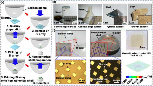
Figure 3. Additive stamp printing with a pneumatically inflated elastomeric balloon as a conformal stamp to fabricate various 3D curvy electronics, reproduced with permission from [35]. (a) Schematic to show the use of a pneumatically inflated elastomeric balloon as a conformal additive stamp. (b) The serpentine metal mesh on convex edge, concave edge, pyramid, and uneven surfaces. (c) The retrieved 39 × 39 Si pellet array (each pellet of 100 × 100 µm) on a balloon stamp and printed on a hemispherical shell, with high yield (>99%) and small strain (0.01%) in all the Si pellets. Reprinted by permission from Springer Nature [72] Copyright © 2019, The Author(s), under exclusive licence to Springer Nature Limited.
Download figure:
Standard image High-resolution imageThe conventional transfer printing can also be combined with the concept of Cartan development to transfer substrate-free, large-area electrodes onto 3D curvilinear skin surfaces without distortion or wrinkles [72] (figure 4). As the sphere rolls along a planar path, the 3D curve from the contact provides the transformation of the curve from the planar surface to the sphere (figure 4(a)). As a result, the cm-long serpentine filaments with a thickness of 1.2 µm and a width of 300 µm can be conformally printed onto a spherical surface. Similarly, complicated 2D patterns with serpentine filamentary elements can be transfer printed onto the spherical surface with slight deformation due to the finite width. Since the Cartan curve does not need to be extensible, a bendable and inextensible cloth donor substrate can be further used to reduce the tensile strain in the filamentary elements during transfer printing. As a demonstration, the 2D cross pattern with four branches on the wet cloth substrate can be transferred to a liquid adhesive hemispherical shell by sequentially laminating and printing only one branch (while avoiding contact with the other) at a time (figure 4(b)). Compared to direct transfer printing, the Cartan transfer printing can conformally print large-area tattoo-like electrodes onto developable skin surfaces (e.g. arms and male chests) and the nondevelopable neck region with little distortion or detachment (figure 4(c)).
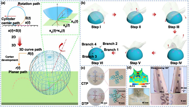
Figure 4. Cartan transfer printing (CTP) to transfer large-area tattoo-like electrodes from a bendable cloth donor substrate to the non-developable neck skin region, reproduced with permission from [72]. (a) Schematic of the CTP and (b) its step-by-step processes. (c) Patterns transfer printed by CTP and direct transfer printing (DTP). (d) Large-area tattoo-like electrodes laminated on the neck through CTP with Gaussian curvature map of the neck, and large-area epidermal electrodes with/without substrate attached on forearm under 180-degree rotation. From [72]. Reprinted with permission from AAAS.
Download figure:
Standard image High-resolution imageInstead of improving the integration method to achieve conformal manufacturing, the flexibility of nanomaterials can be exploited for integration. The unique advantages of functional nano-membranes/materials in conformal electronics and nanotransfer printing is particularly important for the integration of nanomaterials on unconventional substrates. By using a wet-responsive and biocompatible smart hydrogel adhesive, a nanoscale crack sensor can be transfer printed onto a bovine eye [73] (figure 5). The stimuli-responsive and reconfigurable adhesive is fabricated by a replica molding technique using poly (ethylene glycol) dimethacrylate (PEGDMA) as a base material (figure 5(a)). The adhesive exhibits a controllable and switchable adhesion with a high adhesion strength of ca. 191 kPa in a dry state and ca. 0.3 kPa in the swollen state (figures 5(b) and (c)). Its performance can also be maintained under repeated cycles of swelling and deswelling, demonstrating the capability in nanotransfer printing. The fabrication of the nanocrack sensor starts with the formation on a Si wafer, followed by the transfer onto the PEGDMA hydrogel with strong adhesion in a dry state. After bringing the hydrogel with the nanocrack sensor into contact with the bovine eye, saline solution is applied to induce low adhesion in the hydrogel for printing onto the spherical surface of the bovine eye. The transferred nanocrack sensor (of 100 nm wide and 35 nm thick) consists of a 20 nm-thick Pt nanomembrane on a 2 μm thick SU-8 micromembrane in a honeycomb shape (figure 5(d)). The changes in conductive pathways and the resistance of the crack sensor in response to intraocular pressure (IOP) results in the measurement of IOP for the evaluation of patients at risk of glaucoma. The characterizations of the sensor show high sensitivity for a sweeping speed of 0.4 mmHg s−1 during loading and unloading at different IOPs (i.e. 10, 20, 30, and 40 mmHg) (figure 5(e)). The transferred sensor also remains conformally attached to the substrate without delamination even after the repeated cycling loads. Different from PEGDMA, the poly (2-hydroxyethylmethacrylate) (PHEMA) hydrogel adhesive exhibits even stronger adhesion and higher reversibility (adhesion strength of 2.3 GPa/180 kPa in dry/hydrated state) [103], which can also conform to flat and rough target surfaces.
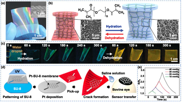
Figure 5. Nanotransfer printing with a smart hydrogel adhesive to fabricate a nanoscale crack sensor onto a bovine eye for detecting intraocular pressure, reproduced with permission from [73]. (a) The fabricated wet-responsive and reconfigurable poly(ethylene glycol) dimethacrylate (PEGDMA) adhesive, where the inset is an SEM image of the PEGDMA nanostructure array of the adhesive. (b) The reversible hydration and dehydration processes of the PEGDMA array. (c) The hydration-induced spontaneous bending of the PEGDMA adhesive film and re-flattening of the adhesive during dehydration. (d) The fabrication of the nanoscale crack sensor and its subsequent transfer printing onto a bovine eye using the PEGDMA adhesive with saline solution. (e) Normalized resistance variation showing the reversible loading-unloading behavior at different pressures. [74] John Wiley & Sons. © (2018) WILEY‐VCH Verlag GmbH & Co. KGaA, Weinheim.
Download figure:
Standard image High-resolution imageIn addition to trigger the response in the above example, the water (vapor or moisture) can also assist the transfer printing process to rapidly fabricate silk antennas onto curved substrates [104] (figure 6(a)). After exposing the back surface of non-crystalline functionalized silk films to water vapor, the film is partially melted and the glass transition temperature of the silk is also lowered. By using gentle pressure, the partially melted and softened adhesive silk film with the Au antenna can be conformally attached to various target surfaces, including eggs, tomatoes, and apples. The antenna transferred on fruits such as bananas can monitor the ripening process. As bananas go from all green at day 0 to fully ripened by day 9, the resonance frequency of the antenna shifts from 36.1 MHz to 42.6 MHz, which results from the geometric deformation and the change in the dielectric properties during ripening (figure 6(b)). By using a water-soluble silk film as the supporting layer for the fabrication of a 32-electrode array, the dissolution of the silk film allows the electrode array to conformally wrap around the highly convoluted surface of the brain cortex (gyri and sulci) for electrocorticogram measurements [37].
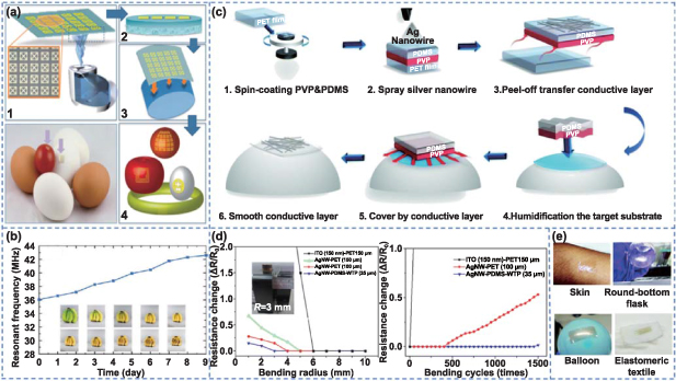
Figure 6. Water-assisted transfer printing. (a) Transfer printing with water vapor to rapidly fabricate silk antennas on curved substrates. (b) Experimentally measured time-dependent resonant frequencies of the silk antenna while the banana ripened over 9 d. (a) and (b) [105] John Wiley & Sons. Copyright © (2012) WILEY-VCH Verlag GmbH & Co. KGaA, Weinheim. (c) Water-assisted transfer printing to fabricate AgNW-PDMS electrode on a polyvinylpyrrolidone (PVP) sacrificial layer onto curves surfaces without sliding or detachment. (d) Relative change in the resistance of ITO on PET, AgNW on PET, and the AgNW-PDMS electrode using this printing method as functions of the bending radius (left) and bending cycles for a bending radius of 4 mm (right). (e) The stretchable conductive electrode can be transferred to various non-conventional substrates, including the skin, a balloon, a round-bottomed flask, and an elastomeric textile. (c)–(e) Reproduced from [106] with permission of The Royal Society of Chemistry.
Download figure:
Standard image High-resolution imageAnother example is the water-assisted transfer printing method, which allows the fabrication of transparent AgNW-PDMS electrodes onto various arbitrary surfaces without the sliding and detachment at the interface [105] (figure 6(c)). The fabrication process starts with spin-coating of PDMS on the sacrificial hydrophilic polyvinylpyrrolidone (PVP) layer, followed by the plasma treatment and spraying of AgNW on the PDMS. Wrapping the composite layer around the pre-humidified target surface dissolves the PVP. The exposed PDMS layer not only provides strong adhesion to either polished smooth surfaces or rough surfaces, but also helps to maintain the electrical property of the AgNW-PDMS electrode after transfer. Compared with the solvent etchable organic transfer process, this is a green chemical transfer process using deionized water and the fabrication process is rapid (3–4 s for electrode being separated from a donor substrate in the water at room temperature). The AgNW-PDMS electrodes in the resulting semitransparent and wearable LEDs showcase a low sheet resistance of 9 Ω sq−1 and high transmittance of 82%. Compared to the significantly increased resistance of ITO on PET (8 folds after 30 bending cycles) and AgNW on PET (2 folds after 450 bending cycles), the AgNW-PDMS electrode only shows a resistance increase of 1.5% after 1500 bending cycles with a 4 mm radius, demonstrating improved electromechanical characteristics (figure 6(d)). This rapid water-assisted transfer printing approach can also integrate thin-film devices to textiles, round-bottomed flasks, balloons, and skin (figure 6(e)).
Though the thickness of nanomaterials is small, the substrate is often much thicker. As a result, the bending stiffness of the composite structure is significantly increased, leading to reduced flexibility and poor contact quality between the device and the 3D surface in the nanotransfer printing. Efforts to address this challenge have resulted in the development of a water transfer printing (WTP) method to fabricate an array of metallic patterned layers on curved dielectric surfaces [74] (figure 7(a)). A periodic array structure with a unit cell of 7.2 × 7.2 mm is first fabricated on polyvinyl alcohol (PVA) substrate by screen printing as a frequency selective surface (FSS) metallic pattern. The WTP process starts with gentle placement of the FSS/PVA composite structure on the water. After the PVA substrate is dissolved, the thin metallic patterns can still float on the water surface due to the water surface tension. Next, a slow dipping process of 3D structures transfers complicated 2D FSS patterns onto the surface of the 3D structure. In the dipping process, the liquid provides proper resistance to ensure the pattern is successfully transferred and conformed to the 3D structural surface. The dissolution of the PVA substrate removes the planar substrate, which allows the FSS unit cells on the water surface to conform onto the non-developable surfaces (e.g. donut-shaped or semi-spherical objects) (figure 6(b)). In contrast, the conventional thermoforming process with the FSS patterns on a polyethylene terephthalate (PET) substrate often results in wrinkles and folds due to the transformation from the developable planar surface to the non-developable ones. Since the simple WTP method can effectively transfer the FSS elements onto the complex surfaces at low cost, it likewise has the potential to fabricate large-scale 3D electronic devices such as massive multiple-input multiple-output (MIMO) antenna arrays.

Figure 7. Water transfer printing. (a) Water transfer printing to fabricate an array of frequency selective surface (FSS) metallic pattern layers on curved dielectric surfaces. (b) The fabricated 3D FSS on the complex structures, including a donut-shaped object and a semi-spherical object. (a) and (b) reproduced from [104]. CC BY 4.0. (c) Adapted water transfer printing with rigid film guides on the edges of the substrate to avoid folds. (d) PVA dissolution behavior with unlined aluminum patterns designed in a star configuration. When the PVA is dissolved, each line composing the star can move and the pattern is deformed (top). When an additional layer of SU8 is printed on aluminum and designed in a square mesh configuration, lines cannot move and the patterns are not deformed (middle). Due to the additional added film guides in the periphery of the PVA substrate, radial forces are drastically reduced to ensure pattern accuracy (bottom). (c), (d) reprinted with permission from [107]. Copyright © (2017) American Chemical Society.
Download figure:
Standard image High-resolution imageWhen the surface of the 3D object is dipped perpendicularly into the liquid, the Stokes flow occurs to result in subtle pattern distortions in the transferred patterns on complex surfaces. For unconnected patterns, the dissolution first started at the PVA edges creates a radial force and leads to pattern deformation. While the SU8 polymer mesh can be used on the unconnected patterns to avoid the pattern movement, the increased bending stiffness of the multilayer structure reduces the level of conformal wrapping with increased folds. As an alternative, the issue can be addressed by using a rigid film guide on the edges of the PVA substrate in the WTP process [106] (figure 7(c)). Because the rigid film guides on the edge of the PVA substrate ensure a comparable dissolution in the PVA to reduce the radial forces, pattern deformation is drastically reduced. Without using an additional mesh layer, this adapted WTP process is particularly helpful to maintain the unlinked patterns while avoiding folds (figure 7(d)). During the dissolution step, a three-axis machine coupled with a visualization system is also used to improve the alignment accuracy between the patterns and target 3D object to millimeter (maximum distortion of 9%).
3. Direct conformal printing techniques
The commonly used direct printing methods include curved lithography, direct laser printing, conformal inkjet printing, and direct ink writing. The representative curved lithography techniques applicable to 3D surfaces with high patterning resolution include holographic lithography (with hologram mask or optically functional prism) and soft lithography (e.g. microcontact printing, nanoimprint, and micromolding in capillaries). However, this class of techniques is challenging for the curved surface over a large area [107]. In direct laser printing [108], laser printing and laser ablation are two commonly used methods to produce patterns on 3D substrates. As for the conformal inkjet printing that dispenses ink droplets onto 3D surfaces, it also includes a broad range of printing techniques, including piezoelectric inkjet printing, aerosol jet printing, thermal bubble jet printing, and electrohydrodynamic printing. In addition to printing 3D self-supporting Ag interconnects/electrodes [109], the direct ink writing can also dispense concentrated Ag nanoparticle inks to fabricate 3D electrically small antennas on curvilinear surfaces for improved gain, efficiency, and bandwidth [110]. Similarly, direct ink printing can also be used to fabricate a broad array of 3D radiofrequency passive components (e.g. inductors, capacitors, interconnections, resonant networks, and metamaterials) for chip-scale radio-frequency electronics [111]. Furthermore, various additive (or layered) manufacturing (or freeform fabrication) techniques [112] have been explored to fabricate thin-film devices on complex 3D geometries (e.g. material extrusion [113] with sintering [114]).
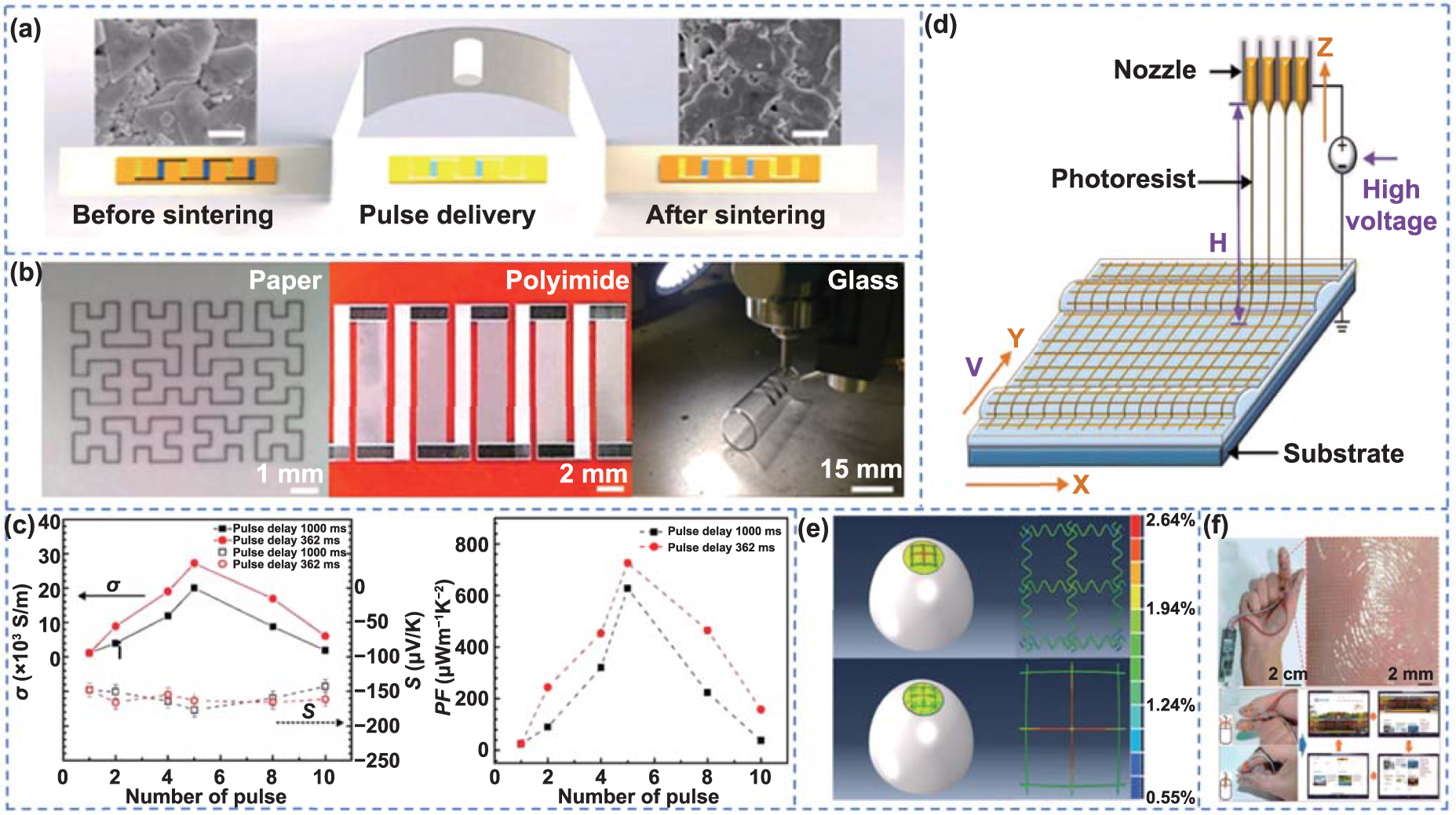
As a high-resolution method with feature size down to 10 µm, 3D conformal aerosol jet printing can precisely print thermoelectric patterns using Bi2Te2.7Se0.3 nanoplate inks on planar and 3D surfaces [115] (figures 8(a) and (b)). The printed film thickness can be precisely controlled by the mass flow rate of the ink and the number of printing passes. Though it is simple compared to other complex fabrication methods (e.g. vacuum filtration [116] and spin/spray coating [117]), the printed film with nanoparticles/plates has reduced density and needs to be sintered. As a high sintering temperature of >400 °C is often required [118], the flexible and stretchable plastic and elastomeric substrates with a low melting point (e.g. 370 °C for PET and 230 °C for PVC) would be damaged. The rapid photonic sintering from intense pulsed light can facilitate densification and grain growth of nanoparticles to significantly enhance the electrical conductivity to  within seconds while localizing the energy without damaging the underneath substrates [119]. The resulting thermoelectric device exhibits an improved power factor of 730 μW m−1 K−2 within seconds, compared to the screen printed Bi2Te2.8Se0.2 of 560 μW m−1 K−2 [120] and the dispensed Bi2Te3 + Epoxy, 280 μW m−1 K−2 [121]. The rapid process is also compatible with highly scalable roll-to-roll printing of thermoelectric devices on low-temperature substrates in 3D curved shapes such as a glass tube. The small increase of 10% in the electrical resistance for a bending radius as small as 1.5 mm indicates mechanical flexibility and robustness of printed thermoelectric films for thermal energy harvesting on curved surfaces (output voltage of 25 mV for a temperature difference of 50 K) (figure 8(c)).
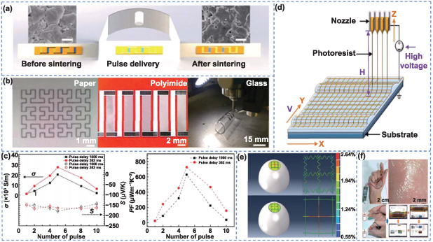
Figure 8. 3D conformal aerosol jet printing and electrohydrodynamic direct writing with a programmable control process. (a) 3D conformal aerosol jet printing with rapid photonic sintering to fabricate thermoelectric films using Bi2Te2.7Se0.3 nanoplate inks on 2D paper, polyimide, and 3D glass tube. (b) The as-printed films with designed patterns can be printed on various planar and 3D substrates. (c) Electrical conductivity (left) and power factor (right) as a function of the number of pulses for the samples sintered under optimized power density of 5.1 kW cm−2, pulse duration of 1.5 ms, and two different pulse delay times of 1000 and 362 ms. (a)–(c) [117] John Wiley & Sons. © (2019) WILEY-VCH Verlag GmbH & Co. KGaA, Weinheim. (d) Electrohydrodynamic direct writing with a programmable control process to fabricate conformable metal-network electrodes in both linear and serpentine patterns on a spherical surface with a radius of 2 mm. (e) Linear and serpentine photoresist pattern and corresponding network electrodes on the spheroid surface. (f) Fingertip touch mouse based on the flexible and transparent electrodes. (d)–(f) [124] John Wiley & Sons. © (2018) WILEY-VCH Verlag GmbH & Co. KGaA, Weinheim.
Download figure:
Standard image High-resolution imageThe electrohydrodynamic direct writing can also be combined with a programmable control process as programmable electrohydrodynamic lithography to fabricate conformable metal-network electrodes [122] (figure 8(d)). The electrohydrodynamic direct writing with a three-axis simultaneous-motioned technique can precisely print a photoresist network pattern on top of the Au/Cr layer on the curved PET substrate with µm resolution. The positioning of printed linear photoresist patterns can be enhanced by using short nozzle-to-substrate distance via a high-speed moving stage [123]. Serpentine patterns with various amplitudes and wavelengths can be printed directly by using the 'whipping/buckling' phenomenon of the electrospinning jet [42] (figure 8(e)). Annealing the printed photoresist patterns for 10 min at 40 °C improves adhesion to the metal layer. Compared to the linear pattern with a strain of >2.5% in most areas (exceeding the yield strain of 2%) on a spherical surface with a radius of 2 mm, only a negligibly small area in the serpentine pattern has a strain exceeding the yield stain (50 nm-thick Au and 1.5 μm-think PET). These metal-network electrodes can conformally attach to finger touch mouse and the skin due to van der Waals force (figure 8(f)).
By transforming the 3D surfaces into a plurality of 2D triangular patches, a five-axis printing system with a single nozzle can print Ag inks on the 3D surface. Similar 2D printing fabricates conformal array microstrip antenna, which avoids the problem of undried conductive flow [12] (figure 9(a)). After each 2D triangular patch is rotated to horizontal based on its normal vector (figure 9(b)), microdroplet inkjet printing [68] on the 2D patch easily reduces printing complexity while preventing the flow of undried ink for improved printing accuracy. By adjusting and optimizing the spacing between circular ink-droplets in the motion command, a boundary-alignment-optimization algorithm can further enhance the uniformity of the printed conductive pattern boundaries. With an energy density of 17.9 J cm−2 and a frequency of 3 Hz in the flashlight, the rapid and low-temperature sintering provides a highly conductive trace (69 870 S cm−1) for microwave applications. A 2 × 4 microstrip antenna array in the experiment shows a return loss of −23.03 dB at 23 GHz with a bandwidth from 12.37 to 13.11 GHz (<−15 dB), consistent with simulation results. This rapid and low-cost printing method to fabricate microstrip antennas on the sphere compares favorably with the holographic lithography technique [124].
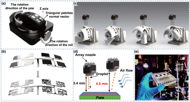
Figure 9. Five-axis printing systems for conformal microstrip antenna fabrication. (a) Schematic of a five-axis printing system. (b) The conversion of the 3D surface into a polarity of 2D triangular patches. (c) Five-axis inkjet printing system with arrayed nozzles. (d) A schematic to show the air drift from the airflow. (e) The fabricated conformal microstrip antenna array with four units. (c)–(e) reproduced from [76]. CC BY 4.0. © (2020) by the authors.
Download figure:
Standard image High-resolution imageComparing the single nozzle employment in planar printing [125], a simultaneously operated nozzle array with over 300 integrated nozzles can enhance the printing efficiency about 100 times while maintaining the same level of accuracy. The five-axis inkjet printing system can also integrate arrayed piezoelectric nozzles to enhance the printing efficiency on the curved surface [75] (figure 9(c)). The inkjet printing with an arrayed nozzle on complex surfaces is still challenging because of air drift/flow and varied height between the nozzle and the landing point on the 3D surface. The result, in fact, indicates that the effect from the airflow and air drift is large if the height is over 3.4 mm (figure 9(d)). The maximum spreading diameter of the droplet on the 3D surface is also larger than that on a flat surface, though it can be calculated based on the weber number and static contact angle. Nevertheless, a maximum fall height of 3.4 mm and a maximum spreading radius of 80 μm can be selected to minimize the negative effect. A conformal microstrip antenna array with 4 units (12.4 × 10 mm for each) can be rapidly printed on a curved dielectric substrate within 5 s (figure 9(e)), which shows a return loss of −15.6 at 6 GHz and a bandwidth of [5.85, 6.1] GHz (−10 dB).
Because of the dependence on the open-loop, calibrate-then-print operation process, most 3D printing methods are limited to static target surfaces (e.g. 3D printed tactile sensor on a model hand [126] and microfluidic device on whole organ models [127]). By exploring computer-vision-based closed-loop feedback control, real-time estimation of the rigid-body motion of the target surface can be combined with the sampled geometric information as feedback to a motion controller for printing on freely moving surfaces [76] (figure 10(a)). The multifunctional devices can be autonomously fabricated with 3D printed electrical interconnects and automatic pick-and-placing of surface-mounted electronic components (figure 10(b)). This real-time tracking of rigid-body motions of the target surface is effective for moving objects without surface deformations. However, it does not consider the dynamically complex deformation of the surface. Efforts to address this challenge have led to the development of an AI-powered printing system that can adapt to the deformation and motion of the target surface in real-time [128] (figure 10(c)). The core concept is to implement offline shape learning and online computer vision-based tracking in the 3D printer integrated with a visual sensing system for tracking the dynamic 3D geometry. The in situ 3D printing system can directly fabricate an electrical impedance tomography sensor (figure 10(d)) on soft surfaces such as a deformable porcine lung in real-time. An ionic hydrogel is also incorporated in the sensor to increase the mechanical compliance for interfacing with the tissue surface. In order to maintain a stable hydrogel–electrode interface under repeated lung expansion and contraction, copper electrodes are embedded in a soft silicone ring that forms chemical bonds with the hydrogel. Though the porcine lung undergoes continuous deformation with a respiration rate of 12 beats min−1, the mean printing error is only 0.657 mm, which provides a continuous spatial mapping of the deformation (figure 10(e)).

Figure 10. Direct printing on freely moving objects in real-time. (a) A hybrid manufacturing process that combines surface-mounted electronic components with directly printed electrical interconnects on freely moving hands. (b) Fiducial markers placed around the automatically pick-and-placed LED on a human hand (left). The adaptive 3D printing of the wireless device on a human hand that can move freely in the workspace (right). (a) and (b) [77] John Wiley & Sons. © (2018) WILEY‐VCH Verlag GmbH & Co. KGaA, Weinheim. (c) An in-situ 3D printing system to directly fabricate an electrical impedance tomography (EIT) sensor. (d) The layered design of the hydrogel-based EIT sensor. (e) In situ 3D printing of hydrogel ink on a porcine lung, with the tracking error as a function of time (mean of 0.657 mm). (c)–(e) from [128]. Reprinted with permission from AAAS.
Download figure:
Standard image High-resolution imageThe conformal direct printing can also be combined with a layer-by-layer soft molding process to fabricate stretchable multilayered tactile sensors [129] (figure 11(a)). Direct printing can print low to highly viscous materials [130] as the elastic body structure and then piezoresistive nanocomposites can be fabricated layer by layer for embedding as the sensing elements for the tactile sensor. By using a conformal printing algorithm, the nozzle can print uniform filaments on inclined flat and 3D surfaces (figure 11(b)). With the conformally printed multilayered tactile sensor consisting of two layers of 8  8 orthogonally printed sensing elements (figure 11(c)), the locations of the applied force on the 3D surface can be detected after using a pressure mapping algorithm.
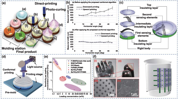
Figure 11. Direct printing using stereolithography. (a) Conformal direct printing with soft modeling for fabricating stretchable multi-layered tactile piezoresistive sensors on freeform surfaces. (b) Filament width variations in upward and downward printing before (top) and after (bottom) applying a conformal printing algorithm. (c) The proposed mechanically compliant, conformal, and multilayered tactile sensor. (a)–(c) reprinted from [132], Copyright (2015), with permission from Elsevier. (d) Conformal 3D printing based on projection stereolithography. (e) Comparison of relative sensitivity between the chemically functionalized BNNTs-based composite and other piezoelectric/polymer composites. (f) The left shows a printed conformal device on the fingertip of a rubber hand model with SEM images of the device surfaces and chemically functionalized BNNTs/resin composite. The right shows the tactile sensor array of 4  4 on the curved surface of a beaker to capture force distribution. (d)–(f) reprinted from [78], Copyright (2020), with permission from Elsevier.
Download figure:
Standard image High-resolution imageThough the projection stereolithography technique is commonly explored for polymers, it can also be applied to piezoelectric boron nitride nanotubes (BNNTs) nanocomposites in a micro 3D printing process to fabricate convex-shaped tactile sensor array on uneven surfaces [77] (figure 11(d)). Because BNNTs with high thermal and chemical stabilities exhibit strong piezoelectricity, they are promising for force sensing applications. The micro 3D printing system mainly consists of a resin bath, sample stage, and a projection system with near-ultraviolet light of 405 nm. With BNNTs in the photocurable polymer resin, the continuous exposure can solidify the piezoelectric composite according to the sliced 2D images generated from the 3D model. The strong covalent chemical bonds and polymer networks formed between BNNTs and polymer can effectively inhibit the interfacial slippage. As a result, mechanical stress is efficiently funneled to the piezoelectric inclusion for improved stress transfer efficiency between the polymer matrix and piezoelectric BNNTs. The exposure intensity of 20 mJ cm−2 and time of 1 s are optimal for curing a single layer of resin with a thickness of 20 μm. The thickness of 20.19 ± 0.56 μm in the printed 20-layer structure is quite close to the setpoint of 20 μm. Compared to the flat composite with unmodified BNNTs, the micropatterned nanocomposite with 0.2 wt% chemically functionalized BNNTs (by 3-Trimethoxysiilylpropyl methacrylate and HNO3) can increase the interfacial adhesion to improve stress transfer between the polymer matrix and piezoelectric nanofillers. Hence, the achieved sensitivity of 120 mV/(kPa wt%) shows a 10-folder increase (figure 11(e)). A convex-shaped piezoelectric device can be conformally printed on the fingertip of a rubber hand model. Similarly, a curved tactile sensor array of 4  4 can be printed on the curved surface of a beaker for detecting the spatial distribution of the force (figure 11(f)).
4. Other advanced fabrication methods
With good electrical and mechanical properties resulting from its stable hexagonal honeycomb structure, graphene patterned into the predesigned structures can be integrated on complex curved surfaces for applications in flexible electronics, energy conversion, plasmonic, and sensing [131–133]. Polydopamine surface modification of the substrate with a mold, followed by the graphene spraying (figure 12(a)) [134], presents a general route to pattern graphene into complex geometries on various curved substrates of different materials (e.g. polymers, semiconductors, and metals). In brief, the PDMS substrate covered with a PDMS flexible mold is dip-coated in dopamine solution that flows through microfluidic channels in the mold. After peeling off the PDMS mold, the spontaneously deposited polydopamine thin film provides enhanced interfacial adhesion to graphene oxide due to strong covalent attraction [135], which mitigates the performance degradation from delamination at the interface. Next, the graphene oxide dispersion is sprayed on the substrate, resulting in selective deposition on the modified region. After drying at room temperature for 24 h, a chemical reduction to reduce graphene oxide in a hydroiodic acid treatment results in the patterned conductive film. Because this approach also works for complex curved surfaces, various graphene patterns have been conformed onto organ models such as lungs and hearts. The flexible strain sensor array of 4 × 4 that conformally covers the irregular lung model shows tunable sensitivity (gauge factor of 100–2000 at 1% strain) and little hysteresis, which is capable of detecting the strain distribution (figure 12(b)).
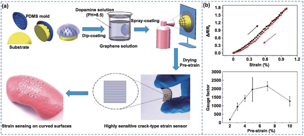
Figure 12. Patterning of graphene on the curved surface, reproduced with permission from [134]. (a) The graphene patterning process for highly sensitive strain sensing on curved surfaces. (b) The top shows relatively small hysteresis characteristic of the sensor in the range of strain 0%–1%, whereas the bottom indicates that different pre-stretch conditions result in varied sensitivities (Gauge factors) of the sensor. Reproduced from [136]. CC BY 4.0. © (2020) The Authors. Nano Select published by Wiley‐VCH [137].
Download figure:
Standard image High-resolution imageBy dispersing functional liquid inks with a modified ballpoint pen through a stencil mask, customizable and deformable electronics can be fabricated draw-on-skin (DoS) with strong adhesion and ultra-conformality [137] (figure 13(a)). After applying the Kapton stencil mask with clear tape on the skin, a modified ballpoint pen with a tip diameter of 1 mm can help draw functional liquid inks at a manual speed of 10 nm s−1. The explored functional liquid inks include conductive Ag-PEDOT:PSS ink, semiconductive P3HT-NK ink, and dielectric ion gel ink. Because of the formed meniscus, the tip of the pen does not need to be in contact with the skin. By using a pen with a finer tip, the line width of the ink pattern can be reduced from 1 mm to 300 μm (with a line space of 200 μm without overlapping by using a stencil). After solvent evaporation for 5 min at room temperature, removal of the stencil leaves the dried sensor pattern on the skin. The resulting electrodes as electrophysiological sensors can still capture high-quality ECG waveform even upon stretching and compression. In contrast, for gel electrodes and mesh electrodes, the mechanical deformation results in sliding (between gel electrodes and skin [136]) and inconsistent adhesion (between mesh electrodes and skin [138]). As a result, the signal-to-noise ratio of 50 dB from the DoS electrodes is much higher than that of gel (20 dB) and mesh (12 dB) electrodes, indicating a small sensitivity to motion artifact on the skin (figure 13(b)).
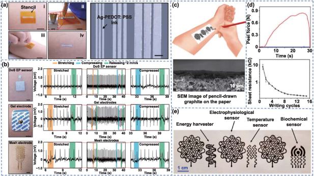
Figure 13. Fabrication of draw-on-skin electronics. (a) Draw-on-skin electronics with functional inks. The line width of the Ag-PEDOT:PSS ink can be controlled by varying the pen tip diameter, where the line widths are 0.3 mm, 0.5 mm, and 1 mm from left to right. (b) DoS EP sensors, gel electrodes, and mesh electrodes with ECG signal recorded upon the skin deformation. (a) and (b) reproduced from [139]. CC BY 4.0. Copyright © (2020), The Author(s). (c) Draw-on-skin electronics by using a 9B sketching pencil on office copy papers. (d) Peel-adhesion test of pristine papers (blue) and papers with spray-coated Silbione (red) on the human forearm, where the stickiness of the resulting on-skin electronic devices can be drastically improved from ∼0.01 to ∼0.85 N after Silbione coating (top). The sheet resistance of the pencil-drawn graphite on papers reduces from ∼10 kΩ sq−1–160 Ω sq−1 as the writing cycle increases from the 1st to 15th cycle (bottom). (e) Pencil-paper on-skin bioelectronic devices.
Download figure:
Standard image High-resolution imageWithout formulating the functional liquid inks, a 9B sketching pencil (93% graphite content by weight) can be used to draw electronics on office copy paper, followed by a back coating of Silbione adhesive for skin contact in a disposable and cost-effective manner [139] (figure 13(c)). Pencil-drawn graphite patterns transferred from the pencil lead to the paper substrate are used as conductive traces and sensing electrodes. For a small weight ratio of 5:100 in Silbione:paper, the adhesion of the on-skin devices is drastically improved from 0.01 to 0.85 N, which allows the devices to stay on arms for more than 3 d. The sheet resistance of pencil-drawn graphite reduces with the number of writing cycles from 10 kΩ sq−1 after the 1st cycle to 160 Ω sq−1 after the 15th cycle (figure 13(d)). The fabricated electronics (e.g. temperature, electrophysical, sweat electrochemical sensors, and humidity energy harvesters) in open-mesh and serpentine layouts can monitor a range of vital biophysical and biochemical signals with performance comparable to their conventional counterparts (figure 13(e)).
Although electronics can be drawn on the skin by the previously discussed methods, there still exist application opportunities to explore highly conductive inks for skin-interfaced electronic devices and soft body area sensor networks that consist of on-body sensors and flexible printed circuit boards. Different from various sophisticated fabrication approaches from lithography and transfer printing [140, 141] to direct printing [142–146], a simple yet universal method has been used to realize the soft body area sensor network (figure 14) [17]. The sintering aid layer consisting of PVA paste and functional nanoadditives (e.g. TiO2, CaCO3) reduces the substrate roughness and the sintering temperature of the stamp-printed metal nanoparticles to lower and even room temperature. The sintered submicron-thick metal patterns using an air blower also show improved electromechanical performance again, bending and folding, which also results in the creation of flexible paper-/textile-based printed circuit boards. Because of the enhanced contact quality between the sintering aid layer and the skin, the sintered Ag electrodes on the skin exhibit lower contact impedance and higher signal-to-noise ratio by ∼20% in the measured EMG/ECG signals when compared to their commercial counterparts (figure 14(b)). In addition to various on-body sensors directly sintered on the skin surface at room temperature, the fabrication approach can also prepare a flexible printed circuit board for signal conditioning/readout and wireless transmission (figure 14(c)). Because of the low mammalian cytotoxicity and good biodegradability, the soft body area sensor network can be easily removed and disposed in warm water flow (figure 14(d)).

Figure 14. Direct sensor fabrication on the skin, reproduced with permission from [17]. (a) The simple process of preparing the directly printed on-body sensors sintered at room temperature. (b) Impedance measurements as a function of frequency from two Ag electrodes of the same size separated by a given distance of 10 cm directly printed and room temperature-sintered on the human skin (left). ECG signals collected using the Ag electrodes on the sintering aid layer with 15 wt% PVA paste (blue) with a larger SNR than those from the commercial electrodes (red) (right). (c) The soft body area sensor network consisting of various on-body sensors (e.g. electrodes and temperature/hydration sensors) and an FPCB. (d) The on-body sensing film can be conveniently removed with negligible effects on the skin by peeling off (top) or washing hands in warm water flow (bottom). Reprinted with permission from [17]. Copyright (2020) American Chemical Society.
Download figure:
Standard image High-resolution image5. Conclusion and future perspective
This mini review briefly summarizes the recent advancement of conformal fabrication techniques for soft deformable sensors and devices on complex curved surfaces (table 1). Combined with stretchable structures and functional nanomaterials, various transfer printing and direct printing techniques are capable of integrating conformal sensors/devices on 3D curvilinear and even dynamically changing surfaces. Advanced transfer printing methods include stamp-based printing, Cartan transfer printing, adhesive-based nanotransfer printing, and water-assisted transfer printing. However, transfer printing techniques have limited efficiency due to multiple transfer steps and the unavoidable pattern distortions during the fabrication process. As an effective alternative to addressing these challenges, advanced direct printing and writing methods have been extensively studied, including inkjet and aerosol jet printing, electrodynamic direct printing, five-axis printing systems, direct ink writing, stereolithography, and DoS electronics. Despite the fact that great strides have been made, many challenges still exist to represent a small fraction for future development in this burgeoning field of conformal electronics on complex 3D surfaces, which is briefly discussed in the following.
- (a)Although it is still challenging to correlate the designed pattern on the 2D surface with that on the curved surface during transfer printing, the computing framework based on the topology method and conformal mapping theory for free-form periodic metasurfaces [147] may be explored. In such a study, after a metamaterial unit cell is designed with tailored, effective properties by using the level-set-based topology optimization, the conformal mapping (or shape-preserving scaling mapping) from each 3D quad mesh surface to the 2D planar unit cell can be calculated. For example, the conformal metasurfaces with different resolutions can be designed and fabricated to conform to a 3D human face (figure 15(a)). The analytical models may also be combined with numerical simulations to study manufacturing variations or help design device parameters (e.g. element spacing in a conformal microstrip antenna array [148]).
- (b)Though a variety of ink has been applied for direct printing of conformal electronics, there is still a wide range of nanomaterials that are challenging to use in fabrication and application. The suspicious cytotoxicity and low dispersity of CNTs in most solvents can be addressed by forming a hybrid with silk sericin that exhibits high biocompatibility, enhanced cell attachment, and good solubility in water [149] (figure 15(b)). The coexistence of hydrophilic and hydrophobic groups within sericin [150] reduces the surface energy and stabilizes the dispersion of CNTs in water, resulting in conductive inks with high stability and biocompatibility. The hybrid ink is compatible with several fabrication methods (e.g. inkjet printing, direct writing, stencil-printing, and dyeing), which has already been explored to fabricate various sensors (ECG electrodes, breath sensors, and electrochemical sensors) on textile, paper, and plastic films.
- (c)It is still challenging to achieve strong and robust adhesion between the soft deformable sensors and the curved surfaces [151, 152]. Inspired by the 'microhair structures' in nature, the bandage-like capacitive pressure sensor with microhair structures mounted on human skin shows a 12 times increase in the signal-to-noise ratio due to the enhanced effective contact area and force transfer between the sensor and the skin [153] (figure 15(c)). Another effective strategy exploits a calcium-modified silk fibroin (figure 15(d)) as a strong, biocompatible adhesive (>800 Nm−1) even upon mechanical deformations (e.g. stretching, compressive, and twisting) [18], which results from the increased viscoelastic property and mechanical interlocking through the incorporation of Ca ions. The reusable, stretchable, and conductive Ca-modified silk can also be used for sensing and hydrogel-based drug delivery.
- (d)There is also an opportunity to explore a set of functional degradable materials [154–159] for conformal transient electronics, including semiconducting [160–163], conducting [164], dielectric materials [165], and substrate and encapsulations [166, 167]. With careful selection of the thickness and materials in the encapsulation strategy, the lifetime of the transient electronics can be programmed before functional degradation [165, 168]. Because of their unique capabilities to safely dissolve after the functional operation, the conformal transient electronics can be used as implantable devices to obviate the additional surgery operations for removal [169] (figure 15(e)). The application opportunities also go beyond the bioimplants to green electronics for sustainable environmental and destructible devices to provide the ultimate device security. It is also worth pointing out that transient electronics can also include those with main constituents to be degradable. As one example, encasing the Ag nanowire-based heater electrode in a biodegradable transparent tape can be conformally mounted on human skin (e.g. wrist, cubital fossa area, and elbow) to allow for visualization of treatment effects without pad removal in thermotherapy applications [36] (figure 15(f)). The fractal heaters with hierarchical architectures maximize the surface area at the microscale for rapid and uniform heating while maintaining high optical transmittance.

Figure 15. Possible directions for future conformal manufacturing. (a) Conformal metasurfaces can conform to a 3D human face, reprinted from [151], Copyright (2018), with permission from Elsevier. (b) Stable and biocompatible carbon nanotube ink mediated by silk protein—sericin, [153] John Wiley & Sons. © (2020) WILEY‐VCH Verlag GmbH & Co. KGaA, Weinheim. (c) Highly skin-conformal microhairy sensor with microhair arrays, [153] John Wiley & Sons. © (2014) WILEY‐VCH Verlag GmbH & Co. KGaA, Weinheim. (d) Calcium-modified silk with strong adhesion induced by calcium reaction, [18] John Wiley & Sons. © (2018) WILEY‐VCH Verlag GmbH & Co. KGaA, Weinheim. (e) A wireless bioresorbable electronic device for nonpharmacological neuroregenerative therapy, reprinted by permission from Springer Nature Customer Service Centre GmbH. [169] Copyright © (2018), The Author(s), under exclusive licence to Springer Nature America, Inc. (f) Fabrication of thermotherapy patch based on fractal-like leaf skeletons (i) using Ag nanowire (ii), reproduced with permission from [36].
Download figure:
Standard image High-resolution image
Table 1. Comparison of different conformal manufacturing techniques.
| Method | Feature | Representative work | Advantage | Limitation |
|---|---|---|---|---|
| Transfer printing | With stamp | Hybrid transfer printing [99] | Simple process with a relatively high yield | Relatively inefficient operation; Possible deformation |
| Additive stamp printing [35] | ||||
| Cartan transfer printing [72] | ||||
| Nanotransfer printing [73] | ||||
| No stamp, but using a sacrificial layer | Water-assisted transfer printing [104, 105] | Simple process and low cost | ||
| Water transfer printing [74, 106] | ||||
| Direct printing | Using functional inks | 3D conformal aerosol jet printing [115] | High precision; Rapid fabrication; High flexibility | Possible thermal damage; Droplet deviation/undried flow |
| Electrohydrodynamic direct writing [122] | ||||
| Five-axis printing system [12, 75] | ||||
| Rea-time direct printing system [76, 128] | ||||
| Projection stereolithography based direct printing [77, 129] | ||||
| Other fabrication methods | Spray coating | Graphene pattern fabrication [134] | Enhanced interfacial adhesion; Easy operation | Limited spatial resolution and pattern accuracy |
| Novel writing tool | Draw-on-skin electronics [137, 139] | |||
| Sintering aid layer | Soft body area sensor networks [17] |
Acknowledgments
The review is written through the contributions of all authors. All authors have given approval to the final version of this review. This research is supported by the National Science Foundation (Grant No. ECCS-1933072), the Doctoral New Investigator grant from the American Chemical Society Petroleum Research Fund (59021-DNI7), the National Heart, Lung, And Blood Institute of the National Institutes of Health under Award Number R61HL154215, and Penn State University. The partial support from the Center for Biodevices, the College of Engineering, and the Center for Security Research and Education is also acknowledged. We also would like to acknowledge the help from Mr. Shangbin Liu in the Cheng Research Group at Penn State University for the creation of schematic illustrations in figures 9(a) and (b). The authors declare no conflict of interest.