
Abstract
Reliable fabrication of micro/nanostructures with sub-10 nm features is of great significance for advancing nanoscience and nanotechnology. While the capability of current complementary metal-oxide semiconductor (CMOS) chip manufacturing can produce structures on the sub-10 nm scale, many emerging applications, such as nano-optics, biosensing, and quantum devices, also require ultrasmall features down to single digital nanometers. In these emerging applications, CMOS-based manufacturing methods are currently not feasible or appropriate due to the considerations of usage cost, material compatibility, and exotic features. Therefore, several specific methods have been developed in the past decades for different applications. In this review, we attempt to give a systematic summary on sub-10 nm fabrication methods and their related applications. In the first and second parts, we give a brief introduction of the background of this research topic and explain why sub-10 nm fabrication is interesting from both scientific and technological perspectives. In the third part, we comprehensively summarize the fabrication methods and classify them into three main approaches, including lithographic, mechanics-enabled, and post-trimming processes. The fourth part discusses the applications of these processes in quantum devices, nano-optics, and high-performance sensing. Finally, a perspective is given to discuss the challenges and opportunities associated with this research topic.
Export citation and abstract BibTeX RIS

Original content from this work may be used under the terms of the Creative Commons Attribution 3.0 license. Any further distribution of this work must maintain attribution to the author(s) and the title of the work, journal citation and DOI.
1. Introduction
Based on Richard Feynman's 1959 lecture 'There is still plenty of room at the bottom, [1] nanoscience and nanotechnology have experienced extensive development in the last 60 years and has become an essential driving force for many technologies, such as integrated circuits (ICs) [2, 3], energy [4–6], medicine [7–10], health monitoring [11, 12], and information storage [13–19]. During the development of nanoscience and nanotechnology, nanofabrication technologies have played the most significant role because they not only enable continuous performance improvements of electronic chips and devices, but also boost the prototyping and realization of other advanced devices, such as photonic [20–24], biomedical [25–27], and quantum devices [28–30]. After decades of development, the frontier of nanoscience and nanotechnology has moved to the sub-10 nm scale where the size effects on the structure properties become more apparent, and there are more available novel functionalities for emerging device applications compared to their macroscale counterparts, which calls for the development of advanced nanofabrication techniques with sub-10 nm resolution and precision.
While the fabrication methods for feature sizes larger than 10 nm are relatively mature, the reliable fabrication at the sub-10 nm scale is much more challenging. Though the node in the latest silicon (Si)-based ICs manufacturing industry has achieved the sub-10 nm scale by combining the most sophisticated lithography, etch, and film deposition processes, the process portfolio in the Si-based IC industry cannot be directly transferred to applications related to the research and development of novel devices because of the extremely high cost and process compatibility [31–34]. For these emerging devices with sub-10 nm features, it is impossible to develop a fabrication process portfolio for all applications because irregular layouts and novel materials are usually involved for different kinds of devices. To satisfy the cost, material, and structure requirements of the devices with sub-10 nm features, researchers have developed various fabrication methods some of which are very specific for certain applications. Considering the significance of nanofabrication techniques on pushing the frontier of nanoscience and nanotechnology, we believe that it is necessary to summarize the existing sub-10 nm fabrication techniques to provide a reference for researchers who work on this research topic.
In this review, we aim to provide a comprehensive summary on the background, techniques, and applications of sub-10 nm fabrication, which includes the following sections: a brief introduction of this review (section 1), the research background and the types of sub-10 nm features (section 2), the collection and categorization of fabrication methods and techniques (section 3), the relevant applications of various sub-10 nm features and structures (section 4), and the remaining challenges and perspectives of this field (section 5). We hope that this review equips researchers with basic knowledge on sub-10 nm fabrication to help them choose appropriate fabrication methods in their fundamental studies and device developments. Particularly, we believe that this review will provide inspirations for researchers who want to develop new nanofabrication techniques to further push the boundaries of science and technology at the sub-10 nm scale.
2. Research background
In the following section, we present the background of sub-10 nm fabrication, including why we are interested in the sub-10 nm scale, different kinds of building blocks with sub-10 nm features, and categories of the fabrication and applications of sub-10 nm structures.
2.1. Why is sub-10 nm fabrication interesting and significant?
The biggest driving force of nanofabrication technology is the IC industry. After decades of development according to Moore's law, the node of the IC industry has reduced to the single-digit nanometer scale. The architecture of field-effect transistors (FETs) has changed from planar to fin FETs. The width of nanofins in the latest complementary metal-oxide semiconductor (CMOS) chips based on fin-FET technology has shrunk to 7 nm (figure 1(a)) [35]. Moreover, the pitch of Si nanofins has also reduced from 60 to 34 nm for FET density scaling, which enables the latest chips with higher performance and lower power consumption. Similarly, sub-10 nm structures and features are also imperative to many non-CMOS devices. Some typical examples include zone plates for x-ray (figure 1(b)) [36–40], nanopore sequencing devices for DNA strands (figure 1(c)) [41–45], superconductor nanowire single-photon detectors (SNSPDs) (figure 1(d)) [46–49], and ultrahigh-frequency surface acoustic wave (SAW, figure 1(e)) resonators [50–52]. In these non-CMOS devices, smaller feature size can either broaden the work range or improve device performance.

Figure 1. The chips and devices requiring sub-10 nm features. (a) The evolution of nanofin width in fin FETs. (b) An x-ray zone plate. From the cross-section view, the width of highest aspect-ratio circular nanowall approaches 10 nm. Scale bar: 2 µm. (c) A sub-5 nm nanopore on a membrane for DNA sequencing. (d) A single unit of a SNSPD. The bottom scheme presents the principle of SNSPD. (e) A scanning electron microscopic (SEM) image of an ultrahigh-frequency SAW resonator. The bottom image depicts the strain of different order harmonic SAWs in the interface between the top interdigital electrodes and the underlying piezoelectric substrate. (a) © (2012) IEEE. Reprinted with permission from [53]. © (2018) IEEE. Reprinted with permission from [55]. The middle electron micrograph is reprinted from the open-access reference [54]. (b) Reprinted with permission from Springer Nature Customer Service Centre GmbH: Springer, Nature Communications [36]. Copyright (2014), Nature Publishing Group, a division of Macmillan Publishers Limited. All Rights Reserved (2014). (c) Reprinted by permission from Macmillan Publishers Ltd. Nature Materials [56]. Copyright (2003) Nature Publishing Group. (d) Reprinted with permission from [47]. Copyright (2011) American Chemical Society. (e) Reprinted from [50], with the permission of AIP Publishing.
Download figure:
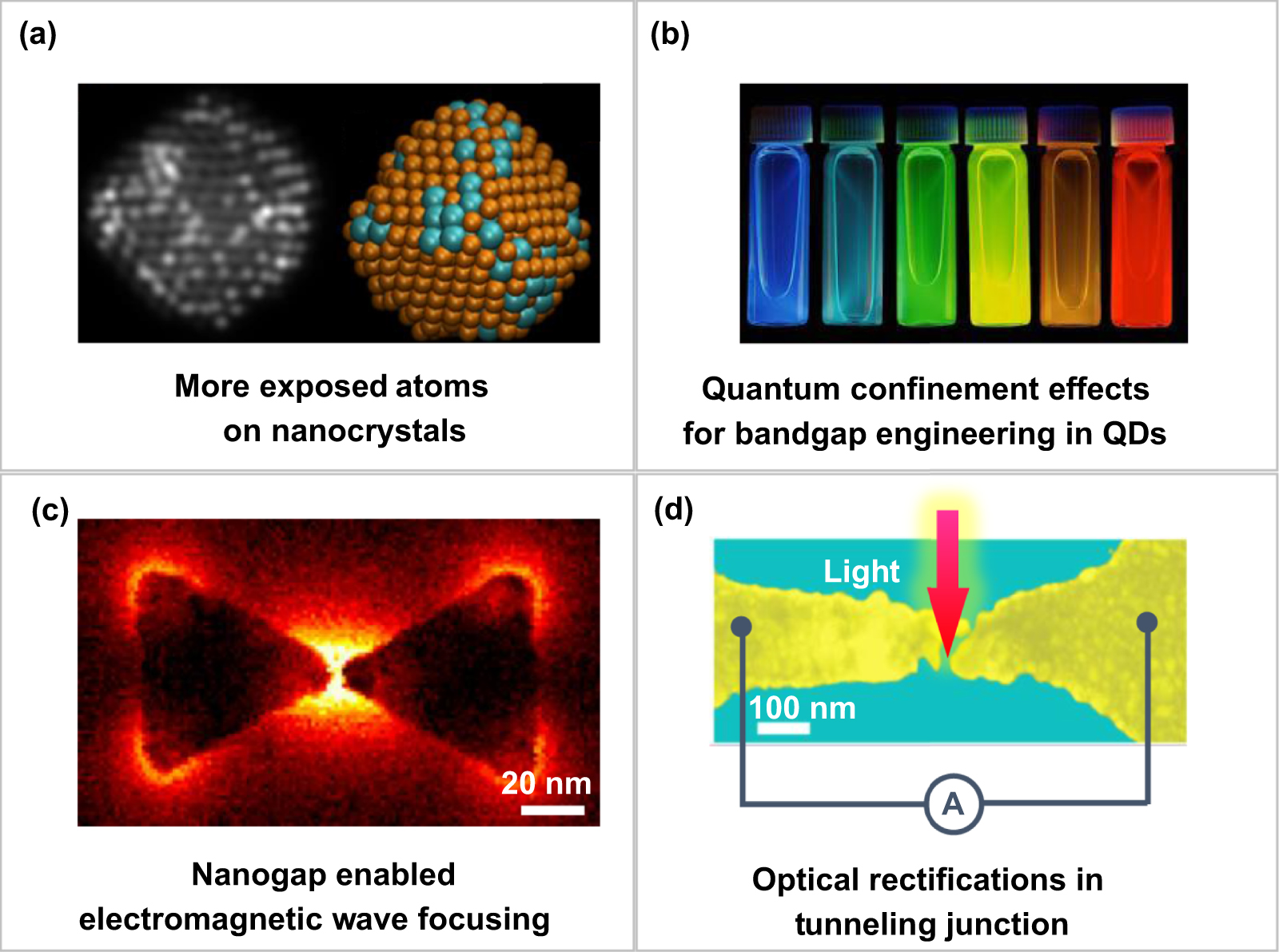
Standard image High-resolution imageIn addition to the above-mentioned functional devices which have already been commercialized, the materials and structures at the sub-10 nm scale also bring many novel and interesting properties to emerging nanodevices. Generally, the novel properties at the sub-10 nm scale can either be enabled by the structure size or by the gap between the structures. The nanoparticles and nanocrystals of sub-10 nm structures have much larger specific surface area compared to their bulk counterparts. Plenty of unpaired electrons on the surfaces and the exposed facets on such small nanocrystals are supposed to significantly promote their chemical reaction and catalytic performance (figure 2(a)) [57]. More importantly, the bandgap of the semiconductor nanocrystals (i.e. quantum dots) can be finetuned by varying their sizes at the single-digit nanometer scale (figure 2(b)) [58, 59]. Sub-10 nm gaps can tune physical properties via the strong resonant energy coupling and tunneling of electrons [60]. On the one hand, sub-10 nm gaps can serve as a cavity that enables extreme electromagnetic-wave confinement into a volume (figure 2(c)) [61], which can strengthen weak light-matter interactions for single molecule and nonlinear spectroscopy [62–65]. Furthermore, sub-10 nm gaps are important building blocks for information processing devices, such as transistors and tunneling junctions (figure 2(d)) [66–72].
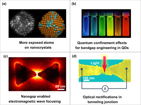
Figure 2. Novel properties of the structures via sub-10 nm size and gaps. (a) Pt-doped Au nanocrystal and the corresponding 3D model. (b) The photoluminescence of CdS/CdSe quantum dots with different nanocrystal sizes. (c) The electron-energy loss spectroscopic mapping of a gold nanobowtie with a 1.6 nm gap. (d) Electromigration-prepared light driven diode with asymmetrical tunneling property. (a) Reproduced from [57]. CC BY 2.0. (b) Reprinted with permission from [58]. Copyright (1997) American Chemical Society. (c) Reprinted with permission from [61]. Copyright (2012) American Chemical Society. (d) Reprinted with permission from Springer Nature Customer Service Centre GmbH: Springer Nature, Nature Nanotechnology [69]. Copyright (2010), Nature Publishing Group.
Download figure:
Standard image High-resolution image2.2. Categories of building blocks and their applications
In this review, sub-10 nm fabrication is introduced as an enabling technological platform to extend Moore's law, explore interesting phenomena and effects in fundamental studies, and develop new concept devices, as summarized in figure 3. The applications in IC chips, enhanced spectroscopy, sensing, field emission, genetic sequencing, and quantum devices are presented. The fabrication techniques and methodologies collected in this review fall into three categories: sophisticated lithography techniques (e.g. photolithography, block copolymer (BCP)-based directed self-assembly (DSA), electron-beam lithography, and focused ion beam (FIB)), mechanically enabled approaches, and post trimming of structures, as indicated by some representative structural or processing examples in figure 3. Because certain applications require different kinds of structures with sub-10 nm and atomic-scale features, the main building blocks we will discuss in this review are listed in table 1 to give the readers a more intuitive map of this research area, which includes regular structures (e.g. nanolines, nanodots, nanotips), inverse structures (e.g. antidots, nanopores, nanogaps) and nanodefects. The corresponding potential applications are also listed in table 1. IC-industry-oriented CMOS technology at the sub-10 nm scale is already very mature and has been documented in numerous past researcher papers, therefore, this review focuses on unconventional methods because they not only enrich the methodologies of sub-10 nm fabrication, but also bring complementary merits in terms of resolution, efficiency, and cost compared to the CMOS approaches.

Figure 3. Overview of sub-10 nm fabrication methodologies and their relevant applications. [79] John Wiley & Sons. Copyright (2008) WILEY-VCH Verlag GmbH & Co. KGaA, Weinheim. Reprinted by permission from Springer Nature Customer Service Centre GmbH: Springer Nature, Nature Communications [80]. Copyright (2013) Nature Publishing Group, a division of Macmillan Publishers Limited. All Rights Reserved. (2013). From [81]. Reprinted with permission from AAAS. Reprinted with permission from [82]. Copyright (2006) American Chemical Society. From [83]. Reprinted with permission from AAAS. Reprinted with permission from [84]. Copyright (2013) American Chemical Society.
Download figure:
Standard image High-resolution imageTable 1. Categories of sub-10 nm structures and their possible applications. Reprinted with permission from [61]. Copyright (2012) American Chemical Society [73]. John Wiley & Sons. Copyright (2005) WILEY-VCH Verlag GmbH & Co. KGaA, Weinheim. © (2017) IEEE. Reprinted with permission from [74]. Reprinted from [75]. Copyright (2008) with permission from Elsevier. Reproduced from [76]. CC BY 4.0. Copyright (2015) The Author(s). Reprinted with permission from [56]. Copyright (2003) American Chemical Society. Reprinted with permission from [77]. Copyright (2008) American Chemical Society. Reprinted with permission from [61]. Copyright (2012) American Chemical Society. Reprinted by permission from Springer Nature Customer Service Centre GmbH: Springer Nature, Nature Nanotechnology, [78]. Copyright (2012) Nature Publishing Group (2012).
| Structures and features at the sub-10 nm scale | Schematics | Demonstration | Possible applications | |
|---|---|---|---|---|
| Nanodots |

|

| PbSe quantum dots [73] | Nano-optics/nanocatalysis |
| Nanolines |

|

| Sub-10 nm Si fins [74] | 7 nm node in IC chips/matter-wave phase-modulated components |
| Nanotips |

|

| Scanning tunneling microscope (STM) tip [75] | Field emission/nanoscale confinement/STM |
| Nanoholes |

|

| Gold nanoholes [76] | Extraordinary transmission/single molecule detection |
| Nanopores |

|

| Nanopore sequencing [56] | DNA sequencing/molecular detection |
| Nanochannels |

|

| Nanofluidic sequencing [77] | Nanofluidics |
| Nanogaps |

|

| Plasmonic nanogap [61] | Single electron transistor (SET)/quantum tunneling/biosensing/nanofocusing |
| Nanodefects |

|

| Single-atom transistor [78] | Quantum source/Rabi splitting/single atom transistor |
3. Techniques and methods
In this section, we give a comprehensive review of the techniques and methods for sub-10 nm fabrication. The fabrication techniques are divided into three strategies, including lithography-based approaches, mechanics-enabled approaches, and post-trimming approaches. While the lithography-based approaches are still the mainstream, they suffer from limited resolution and high cost. Mechanics-enabled and post-trimming approaches provide smart solutions that complement the lithography-based approaches and have the advantages of higher resolution or lower cost, especially for fundamental research and non-CMOS device applications.
3.1. Lithography-based approaches
Among various fabrication techniques, lithography is the most commonly used method for patterning because it can define resist structures with large degrees of freedom. In combination with subsequent pattern transfer processes, such as film deposition and etching, additional freedom can be introduced to obtain functional structures. Generally, lithographic methods can be categorized into two main parts: direct methods for pushing the lithography resolution to the sub-10 nm scale, and smart approaches to achieve sub-10 nm features via pattern transfer. The following section introduces these approaches.
3.1.1. Advanced photolithography processes for IC manufacturing.
Photolithography with higher resolution has always been a key topic in IC chip manufacturing. In IC chip manufacturing, photolithography is the preferred patterning solution due to its capability for large-volume production. The resolution is the most significant parameter to evaluate the capability of lithography techniques because it determines the limit of feature size in the follow-up fabrication processes. For a common photolithography system, the resolution of photolithography in modern IC manufacturing is determined by the following equation,

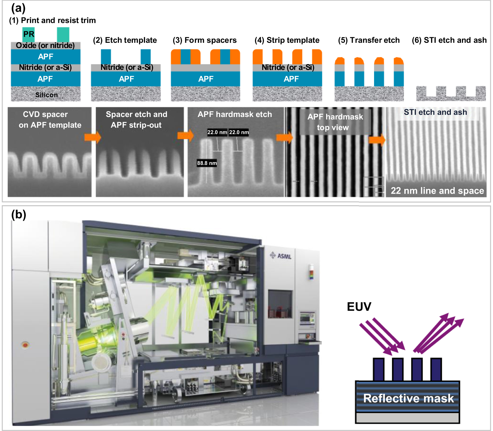
where k1 presents the process factor, λ is the wavelength of illuminated light, and N.A. is the numerical aperture of the illumination system. Clearly, reducing the light wavelength directly improves the resolution. Several resolution enhancement techniques have been developed [85], such as off-axis illumination [86], phase-shifting masking [87], immersion lithography [88], and optical proximity correction [16]. To further scale down the power and FET density of IC chips, the self-aligned double patterning (SADP) technique is used to double the printed line density. This technique involves the use of chemical vapor deposition to grow a sidewall spacer on a core (template) pattern defined by conventional photolithography to create a pitch-halving hard mask [89], as shown in figure 4(a). However, doubling the line pattern density in the SADP process flow makes the process more complex because it requires additional lithography steps and photomasks for trimming closed-loop patterns into individual lines. Self-aligned quadruple [90] and octuple patterning [91] have also been demonstrated to further promote FET density scaling in chips, but the proportion of the lithography cost in the entire IC manufacturing soars to over 50%. Fortunately, extreme ultraviolet (EUV) lithography (λ = 13.5 nm) further increases the power and FET density scaling of IC chips [92, 93]. Higher-resolution patterning based on EUV lithography has been thoroughly developed (figure 4(b)) [94]. However, due to the high cost, EUV lithography is not suitable for device prototyping or small-volume production. For these specific applications, other techniques, such as DSA of BCPs, nanoimprinting and maskless direct writing provide complementary capabilities, which we will discuss in the following sections.
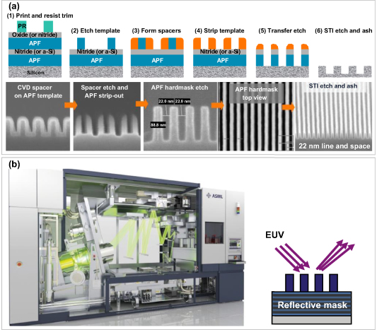
Figure 4. (a) The scheme of SADP based on 193 nm immersion lithography. (b) The EUV lithography. Left picture presents that EUV lithography machine contains a powerful EUV source and a sophisticated set of mirrors. Right image shows the scheme of reflective projection in EUV lithography. (a) Reprinted with permission from [89]. Copyright (2008) Society of Photo-Optical Instrumentation Engineers (SPIE). (b) [94] John Wiley & Sons. Copyright (2009) WILEY-VCH Verlag GmbH & Co. KGaA, Weinheim.
Download figure:
Standard image High-resolution image3.1.2. BCP-based DSA.
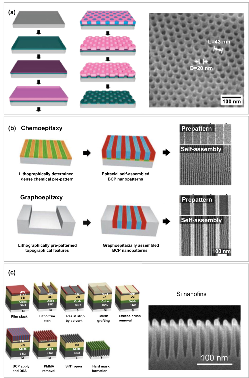
BCP-based DSA is a high-resolution, low-cost patterning technique to generate uniform domain nanostructures in BCP film via the separation of microscale phases, as shown in figure 5(a). The spontaneous process of microphase separation results in BCP microdomain arrays with short-range order. With the implementations of graphoepitaxy or chemoepitaxy via pre-defined physical patterns or chemical contrast [95]. The domain structures of BCPs can be directed to form 'single-crystal' structures in which the position and orientation of microdomains can be determined. Subsequently, one of the separated microdomains can be selectively removed and served as the patterned template for pattern transfer processes, as shown in figure 5(b). Due to the capability of inexpensive processing to attain oriented and periodic structures with long-range order, BCP-based DSA is an emerging lithography process that can advance technology nodes in semiconductor manufacturing. In the current semiconductor industry requires sub-10 nm feature size. Exploring the capability of BCP-based DSA at the sub-10 nm scale usually involves thermodynamic control over the size and morphology of microdomains. Furthermore, the combination of high-resolution lithography technologies (e.g. DUV and nanoimprint lithography (NIL)) can assemble BCPs into essential dense and isolated nanofeatures as currently defined by semiconductor manufacturing [96, 97]. Scientists at IBM evaluated the potential of BCP-based DSA in a 7 nm fin-FET technology node and beyond and compared its performance to that of devices based on current photolithography techniques [98], as shown in figure 5(c). However, the resultant sub-10 nm polymer structures did not possess sufficient etch resistance for subsequent pattern transfer. Subsequential infiltration synthesis (SIS) effectively enhances the etch resistance by converting a specific block in a BCP to inorganic oxides using atom-layer deposition (ALD) [99, 100]. The conversion of sub-10 nm patterns from organic to inorganic material with SIS treatments can be used to strengthen mechanical stability and stiffness, which is significant for the fabrication of large-area nanoimprint molds for nanophotonic and nano-optic applications. However, the defect control of BCP-based DSA is a long-lasting issue for reliable nanopatterning. In particular, the defect level is the key parameter in semiconductor manufacturing with a strict requirement in defect density. Hence, most researchers in this promising technique topic attempt to reduce defect density.

Figure 5. Principle and strategies of the BCP-based DSA technique. (a) A Schematic of self-assembled BCPs for nanopatterning. The right SEM image presents periodic nanoholes (D = 20 nm) that selectively remove the polymethyl methacrylate (PMMA) block in polystyrene-block-polymethyl methacrylate (PS-b-PMMA) after microphase separation. (b) Schematic of DSA of BCPs based on graphoepitaxy and chemoepitaxy strategies and the corresponding results. (c) Process flow of fabricating Si nanofins in 7 nm fin-FET technology based on BCP-based DSA. The SEM image on the right presents the cross section of periodic as-etched Si nanofins based on DSA of BCPs. The lamellar resist patterns are generated by chemoepitaxy DSA of PS-b-PMMA. (a) [79]. John Wiley & Sons. Copyright (2008) WILEY-VCH Verlag GmbH & Co. KGaA, Weinheim. (b) Reprinted from [101]. Copyright (2013), with permission from Elsevier. Reprinted with permission from [102]. Copyright (2015) American Chemical Society. (c) Reprinted by permission from Springer Nature Customer Service Centre GmbH: Springer Nature, Nature Electronics [98], Copyright (2018) The Author(s), under exclusive license to Springer Nature Limited.
Download figure:
Standard image High-resolution image3.1.3. Nanoimprint lithography (NIL).
NIL is performed by pressing a mold with nanoscale patterns onto a flowable polymer or curable monomer and inversely duplicating the mold patterns onto the polymer, as shown in figure 6(a), which is a promising technique for large-volume production, especially for the applications of wafer level optical elements [103, 104].

Figure 6. NIL and typical methods of fabricating sub-10 nm molds. (a) Schematic flow charts depicting the NIL process. (b)–(d) Three main methods to fabricate NIL molds at the sub-10 nm scale using (b) the EBL process, (c) single-wall carbon nanotube (SWCNT), and (d) edge lithography. (e) and (f) Corresponding patterns on a mold and polymer. (g) SEM image of imprinted periodic nanolines on polymer with different pitches. (e) Reproduced from [105], with the permission of AIP Publishing. (c) and (f) Reprinted with permission from [106]. Copyright (2004) America Chemical Society. (d) and (g) Reprinted from [107]. © IOP Publishing Ltd. All rights reserved.
Download figure:
Standard image High-resolution imageDue to its duplication manner in patterning, the resolution of NIL is determined by the feature size on the mold. A number of works have demonstrated that NIL has the capability of achieving sub-10 nm resolution [108–111]. Figure 6(b) schematically presents the fabrication of a sub-10 nm imprint mold by high-resolution patterning based on electron-beam lithography (EBL) or He+-FIB processes [112, 113]. Astin et al fabricated a high-precision Si mold by reactive ion etching (RIE) based on EBL-predefined hydrogen silsesquioxane (HSQ) masks (the left SEM image in figure 6(e)). They subsequently obtained a 5 nm wide nanofin on polymer (the right SEM image in figure 6(e)) [105]. NIL can duplicate patterns down to the 2 nm scale. As depicted in figure 6(c), by using single-walled carbon nanotubes as the original master [106], an isolated inverse channel as small as 2 nm can be duplicated onto a hard polydimethylsiloxane (PDMS) mold. Using the duplicated hard-PDMS mold, a single 2.4 nm wide line can be imprinted on polyurethane (see figure 6(f)). Meanwhile, high-density features with 6 nm half pitches have been obtained using sub-10 nm edge structures in superlattice materials (figure 6(d)) as the molds [107], as shown in figure 6(g). However, for practical large-volume industrial applications, low-cost fabrication of large-area molds with long lifetime and high-fidelity duplication of the features over large areas are still challenging for NIL, especially when involving quasi-3D structures, such as slanted features. Due to defect, reproducibility, and overlay inaccuracy issues, NIL is difficult to apply in the IC industry. As a result, this method is more appropriate for non-IC applications.
3.1.4. Electron-beam direct writing (EBDW).
EBDW is a flexible fabrication technique for patterning without any masks. The most sophisticated EBL systems have the capability to achieve 1 nm scale spot size and even down to the angstrom scale. Such small spot size enables us to achieve high-resolution and high-flexibility patterning based on different principles [114, 115].
For all processes based on EBL, the first step is to obtain ultrasmall resist structures, a typical process flow is shown in figure 7(a). Similar to photolithography, EBL is the most commonly used patterning method based on the EBDW strategy. V Manfrinato et al fabricated sub-5 nm features using 200 kV scanning EBL in a transmission electron microscope (TEM) [116, 117]. In their work, the suppression of electron scatterings is a key factor for achieving such high-resolution patterning by adopting ultrathin resist films and freestanding membrane substrates. Yang et al demonstrated sub-10 nm nested-L features based on an HSQ resist using salty developer with high development contrast [118–120]. The results are shown in figure 7(b). Note that the sub-10 nm features reported in these works are only defined on the resist. High-fidelity pattern transfer is also significant to sub-10 nm fabrication, which is not discussed in this section.

Figure 7. FEB-based fabrication techniques. (a) Process flow of electron beam lithography. (b) Nested L-shaped HSQ lines with 4.5 nm half pitch. (c) Schematic of focused EBID. (d) Tungsten (W)-containing nanodot array with a spacing of 4 nm fabricated by focused electron-beam induced deposition (FEBID) from a W(CO)6 precursor. Fabrication was performed by scanning a focused transmission electron beam at 200 keV. (e) Schematic of nanosculpting enabled by a FEB. (f) Defined nanogap electrode with 0.6 nm separation using electron-beam sculpting. (b) Reprinted with permission from [118]. Copyright (2009) American Vacuum Society. (d) Reprinted with permission from [121]. Copyright (2005) American Chemical Society. (f) Reprinted with permission from [127]. Copyright (2005) American Chemical Society.
Download figure:
Standard image High-resolution imageUnlike lithography, electron-beam induced deposition (EBID) can directly fabricate functional structures, as schematically depicted in figure 7(c). van Drop et al manufactured periodic dots of about 2 nm with a spacing of 4 nm using an environmental TEM (200 kV) equipped with a gas injection system [121], as presented in figure 7(d). In addition, Shen et al reportedly used electron beam healing in TEM to repair two-dimensional MoS2 crystals in-situ [122]. Compared to induced deposition, electron-beam induced etching (EBIE) is used to fabricate inverse nanostructures. Yemini et al presented the smallest nanopore of 17 nm on an Si membrane fabricated by EBIE with the assistance of XeF2 gas [10]. By optimizing the pressure and process rate, a sub-10 nm nanopore could be achieved with an appropriate etching rate. However, limited efficiency and the precursor species impedes electron-beam induced processing for large-area and fast nanopatterning, and the impurities of the resultant structures caused by carbon contamination is an issue in practical applications.
High-energy focused electron beams (FEBs) can perform direct patterning based on atomic-scale sculpting via bombardment, as shown in figure 7(e). Drndic et al performed the nanofabrication of metallic structures and nanodevices on an insulating membrane using transmission FEB sculpting at 200 keV [123–126]. Zandbergen et al also fabricated 0.6 nm gaps in nanoelectrodes using transmission FEB sculpting (figure 7(f)) [127]. An advantage of such processes is that the fabrication can take place in-situ monitoring enabled by high-resolution imaging, thus, high precision can be realized.
3.1.5. FIB techniques.
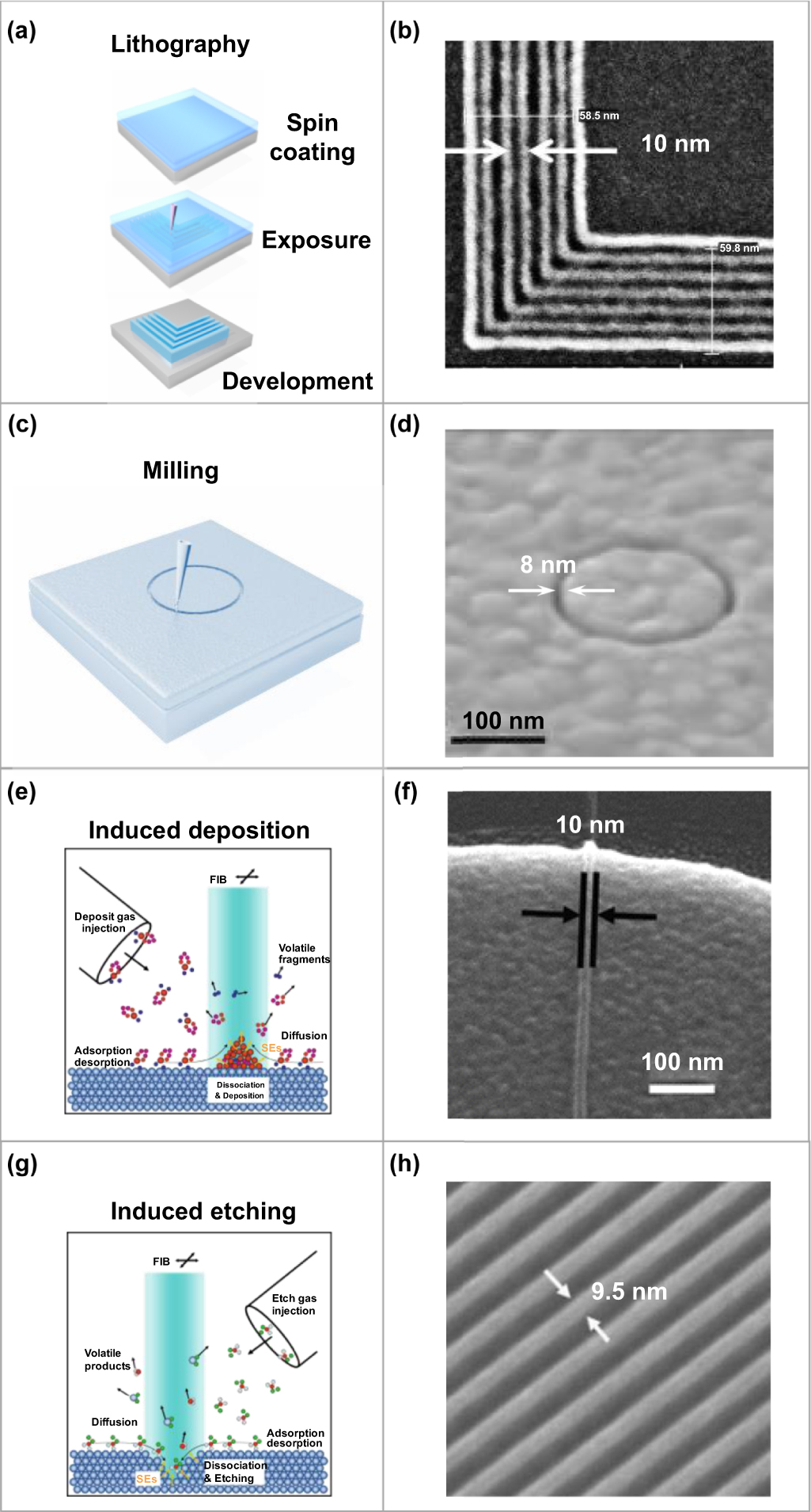
Similarly to FEB-based fabrication techniques, FIB can be used for nanofabrication either via lithography, milling, or induced processing (e.g. deposition and etching) [128]. Extremely small interaction volume is necessary to obtain sub-10 nm fabrication using FIB [129]. Recently, most sub-10 nm fabrication based on FIB utilizes a focused helium ion beam (He+-FIB) due to its sub-nanometer spot size [130]. Less scatterings from the resist and substrate greatly mitigate the proximity effect in high-density FIB patterning compared to EBL. As shown in figures 8(a) and (b), Li et al demonstrated a resolution of 10 nm pitch in nested-L lines using HSQ resist which is difficult to achieve using the EBL process [113]. However, the relatively high line-edge roughness in sub-10 nm features, caused by shot noise, and inevitable damage to underlying materials and substrates are the challenges in lithography based on He+-FIB.

Figure 8. FIB-based fabrication techniques. ((a), (c), (e), (g)) Fabrication schemes of FIB lithography, milling, induced deposition and etching. (b) Nested-L lines with 10 nm pitch fabricated by scanning helium ion lithography on an HSQ resist. (d) Coaxial plasmonic resonator in the shape of an 8 nm wide circular slit on gold film. (f) Focused ion-beam induced deposition (FIBID)-defined single cobalt line with a width of 10 nm between multiterminal electrodes for circuit editing. (h) Periodic 9 nm wide WS2 nanoribbons patterned by XeF2-assisted He+-FIB. (b) Reprinted with permission from [113]. Copyright (2012) American Vacuum Society. (d) Reprinted with permission from [134]. Copyright (2013) American Chemical Society. (f) Reprinted by permission from Springer Nature Customer Service Centre GmbH: Springer Nature, Journal of Materials Science: Materials in Electronics [136]. Copyright (2013) Springer Science Business Media New York (2013). (h) [137] John Wiley & Sons. © (2017) WILEY-VCH Verlag GmbH & Co. KGaA, Weinheim.
Download figure:
Standard image High-resolution imageCompared to the required pattern transfer in resist-based lithography, FIB milling is a direct method to fabricate functional structures via selectively removing materials based on sputtering, as shown in figure 8(c). This advantage makes FIB milling a popular technique for fabricating inverse structures (e.g. holes [131] and slits [132, 133]). The nanometer spot size in He+-FIB enables the reliable sub-10 nm resolution in milled nanofeatures. A high-quality plasmonic resonator based on ring-like slits with 8 nm width was fabricated [134], as shown in figure 8(d). Nevertheless, because the extremely small spot size of a He+ ion beam originates from the singe atom emitter in an ion source [135], the low beam current and lighter ion mass lead to extremely slow fabrication speeds, making this method only feasible for fundamental research.
FIB induced deposition and etching can also be performed for nanoscale structuring, as shown in figures 8(e)–(g). Ultrasmall spot size is crucial to the sub-10 nm resolution in FIB induced processing. As shown in figure 8(f), with He+-FIB, Wu et al presented single cobalt (Co) lines with minimum linewidths of 10 nm using a Co2(CO)8 gas precursor for circuit editing [136]. Meanwhile, Stanford et al reported 9 nm wide WS2 ribbons patterned by XeF2-assisted He+-FIB induced etching [137], as shown in figure 8(h). Similar to lithography and milling processes, damages due to ion bombardment and implantation on substrates and other functional materials are unacceptable in some specific applications, such as electronic devices, which limits the broad application of FIB-induced processes.
3.1.6. Tip-based nanofabrication (TBN).
TBN is carried out by scanning a nanoscale tip in close to a substrate to execute a patterning event initiated by an external stimulus. The local external stimulus can be introduced from thermal, electronic, or mechanical effects or molecular diffusion localized to a nanoscale volume between the tip, with high curvature, and the substrate.
As early as 1993, Crommie et al demonstrated atom manipulation using a STM [138], as shown in figure 9(a). They built a quantum corral where they positioned 48 iron atoms on an atomically flat copper (111) crystal surface under extremely high vacuum and 4 K temperature. In 1999, Lyding et al performed atomic lithography to remove hydrogen atoms from a hydrogen-passivated Si surface with electron stimulated desorption process using an atom-scale tip of STM (see figure 9(b)) [139]. The selective deposition in the depassivated area can be used as a mask pattern for further pattern transfer. With this approach, Si feature sizes as small as 2 nm were achieved.

Figure 9. TBN approaches. (a) Schematic of STM and construction of corral-patterns from the confined surface state of 48 iron atoms on Cu (111) via STM-based manipulation. (b) Schematic of STM-based hydrogen depassivation lithography. (c) Thermal TBN lithography to conduct sub-10 nm patterning on an Si surface. (d) Field-emission TBN for a development-less lithography process on a glass-state calixarene molecular resist. (e) Illustration of DPN method. The AFM image presents a DPN-defined thiol-based molecular nanoline, 30 nm in width, on a gold surface. (a) From [138]. Reprinted with permission from AAAS. (b) Reprinted with permission from [139]. Copyright (2014) American Vacuum Society. (c) Reprinted with permission from [140]. Copyright (2017) American Chemical Society. (d) Copyright (2013) Society of Photo-Optical Instrumentation Engineers (SPIE). (e) From [147]. Reprinted with permission from AAAS.
Download figure:
Standard image High-resolution imageUnlike the extreme working conditions required in STM, atomic force microscope (AFM) has broader applications because it works on dielectric substrates in atmosphere and even solution. Furthermore, various scanning probe lithography (SPL) systems based on AFM have been developed in the later decades. In thermal-based SPL, a resolution of 7 nm half pitch Si features can be achieved via RIE with a thermal SPL defined sub-10 nm polymer/SiO2 mask [140], as presented in figure 9(c). Except for lithography, thermal AFM can also initiate nanoscale chemical reactions, such as reducing oxidized graphene to obtain sub-10 nm semiconductor graphene ribbons. The atomic-scale-sharpness tip not only confines energy to conduct lithography but can also be used to perform resist removal using field-emitted, low-energy electrons from the tip. In figure 9(d), Rangelow's team demonstrated lithographic approaches for 'single nanometer manufacturing' [141–144]. They achieved feature sizes as small as 5 nm on a calixarene molecular glass resist using the electric field current-controlled SPL method [145]. Single ion implantation can also be achieved using a hollow tip and small aperture mounted on a pre-collimation membrane [146], which is supposed to be a key enabling technology for developing quantum devices.
Another important technique in tip-based approaches is 'dip-pen' nanolithography (DPN). DPN was firstly demonstrated by Mirkin's group via delivering alkanethiols molecules from an AFM tip to a gold substrate through capillary transportation [147], as shown in the left graph of figure 9(e). Using this process, 30 nm wide lines were obtained on a gold substrate, as shown in the right picture of figure 9(e). The further work demonstrated the construction of an organic transistor using DPN via selectively positioning organic semiconductor molecules into gap electrodes [148, 149]. In DPN, tip-substrate molecular transport is a complicated process that is influenced by many parameters, such as the tip shape, surface chemistry, the mobility of the ink on the tip, temperature, environmental humidity, and water solubility of the ink.
3.1.7. 'Sketch and peel' strategy.
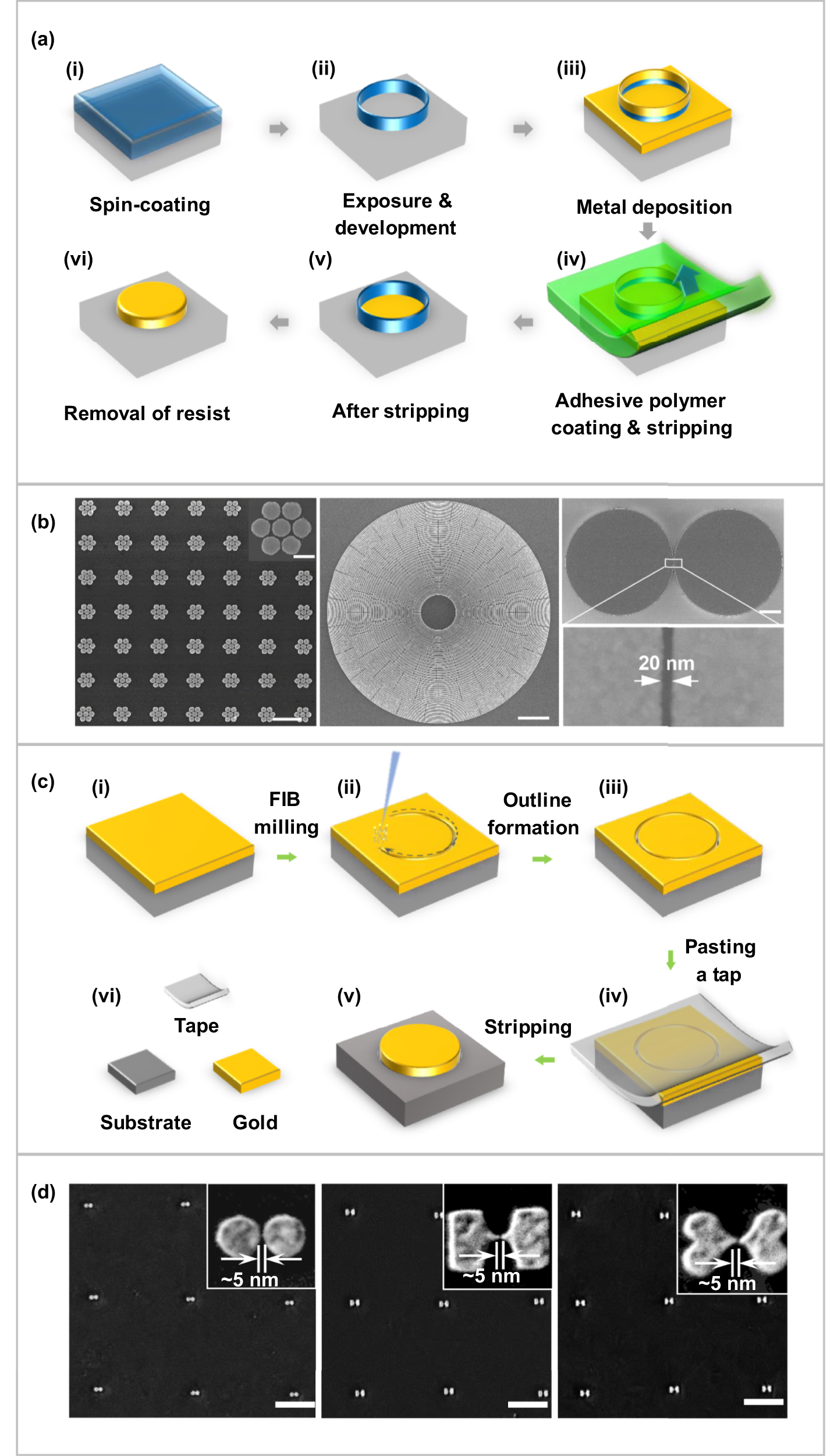
The 'sketch and peel' strategy was proposed by the authors' group in 2016. This is a novel patterning strategy based on serial direct writing techniques. Unlike the conventional strategy which exposes an entire area, the 'sketch and peel' method only exposes the outlines of target structures with a FEB. After film deposition, a stripping step is performed to define the desired structures by selectively removing the outer metallic film, as seen in figure 10(a) [150]. Due to the advantage of outline exposure, the 'sketch and peel' strategy can greatly improve patterning efficiency by more two orders of magnitude and can also mitigate the proximity effect for high-fidelity fabrication of extreme features with sharp corners and nanogaps [151]. In figures 10(b), uniform gap of 15 nm in plasmonic oligomers and nanogap electrodes 20 nm apart were presented in the original work [152–156].

Figure 10. 'Sketch and peel' strategy. (a) Schematic of 'sketch and peel' lithography based on the HSQ-based EBL process. (b) Ultrasmall gold nanogaps fabricated by EBL-based 'sketch and peel' lithography. Scale bars: 1 µm in the left picture; 2 µm in the middle image; 10 µm in the right electron micrograph. The inset in the left is 100 nm. Left panel presents periodic nanoheptamers with uniform gaps of 15 nm; middle panel shows a zone-plate-like optical element; right panel is the SEM image of sub-millimeter-scale electrode pairs and the enlarged electron micrograph of gap region. (c) Schematic of FIB-based 'sketch and peel' lithography. (d) Different-shape dimer array obtained by He+-FIB-based 'sketch and peel' lithography. Disk (left panel), dumbbell (middle panel), heart (right panel). Scale bars : 1 µm. (a) and (b) Reprinted with permission from [150]. Copyright (2016) American Chemical Society. (c) Reprinted with permission from [157]. Copyright (2016) American Chemical Society. (d) [158]. John Wiley & Sons. © 2020 WILEY-VCH Verlag GmbH & Co. KGaA, Weinheim.
Download figure:
Standard image High-resolution imageThe 'sketch and peel' strategy can also be applied in FIB fabrication, except for EBL, which significantly extends the patterning capability of FIB for preparing particle-like structures, as depicted in figure 10(c). For He+-FIB, this novel strategy enables it to possess a patterning capability that was previously impossible. Applying this advanced process, a series of plasmonic assemblies with sub-10 nm gaps have been demonstrated in Chen's work, as shown in figure 10(d) [157, 158].
3.1.8. Smart pattern transfer approaches.
This section summarizes smart approaches in pattern transfer to fulfill the fabrication of sub-10 nm features in devices [159–161]. Sub-10 nm fabrication in these approaches does not depend on the lithographic resolution, which is in contrast achieved via tricky methods or effects including film deposition, angular evaporation, nanometer scale stenciling, secondary deposition, etc.
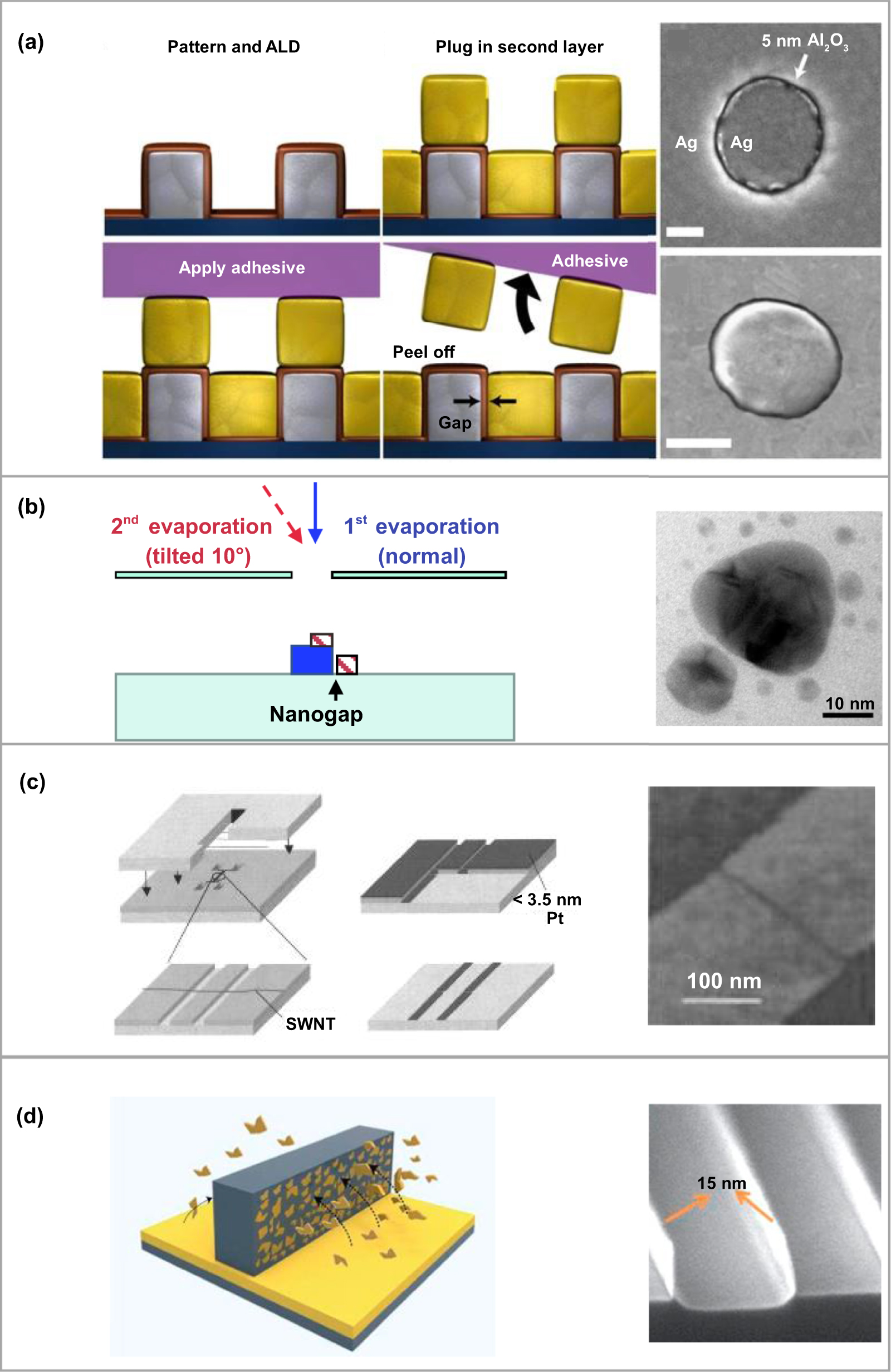
3.1.8.1. Film-defined nanogap.
Film deposition to realize a given thickness is a well-developed technology in nanofabrication. Ultrasmall nanogaps can be defined via edge lithography by involving conformally-coated nanofilm thickness on the sidewall of first patterns to separate the second deposited materials [162], as shown in figure 11(a). The conformal coating is commonly performed by atomic-layer deposition [34]. In addition, the film thickness can also be determined by the length of organic molecules self-assembled on the first-defined pattern. Oh et al demonstrated that edge lithography is robust and scalable for wafer-scale fabrication of sub-10 nm plasmonic gaps and gap electrodes [80]. With this concept, Beesley et al presented that self-assembly monolayers can be used as the separation for sub-15 nm patterning of asymmetric metallic electrodes [163]. Moreover, Mirkin's group developed on-wire lithography in which the gap size was determined by the thickness of one segment on a nanowire grown by electrochemical deposition in anodic oxidization of an aluminum template [164]. The materials in different segments can be selectively removed in the subsequent etching procedure.

Figure 11. Schematics and proof-of-demonstration of smart pattern transfer approaches (a) Schematic of film-defined nanogap fabrication. Scale bars: 300 nm. (b) Schematic of angular deposition. (c) Nanostencil lithography. (d) High-aspect-ratio (HAR) nanowalls defined by secondary sputtering effect. (a) Reprinted by permission from Springer Nature Customer Service Centre GmbH: Springer Nature, Nature Communications [80]. Copyright (2013) Nature Publishing Group, a division of Macmillan Publishers Limited. All Rights Reserved. (b) Reprinted with permission from [165]. Copyright (2010) American Chemical Society. (c) Reprinted with permission from [166]. Copyright (2006) American Vacuum Society. (d) [167] John Wiley & Sons. © (2020) WILEY-VCH Verlag GmbH & Co. KGaA, Weinheim.
Download figure:
Standard image High-resolution image3.1.8.2. Angle evaporation.
Angle deposition utilizes the shadow effect of mask patterns with a tilt angle in the vacuum evaporation process, which can fabricate nanometer gaps as small as 1 nm, as shown in the left picture of figure 11(b). In this approach, two serial angle evaporations have to be performed. The materials in both depositions can be either heterogenous or homogenous according to the specific applications [168, 169]. Using this method, Theiss et al presented sub-10 nm gap fabrication for surface-enhanced Raman spectroscopy [165]. Scientists from IBM demonstrated a 9 nm channel carbon transistor [170]. In this method, ultrahigh vacuum in evaporation is essential to prevent possible bridge formation in the gap region caused by the deflected vaporized atoms colliding with residue gas molecules in the vacuum chamber. In the SEM image of figure 11(b), the tiny dots surrounding the structure provide evidence of such phenomenon.
3.1.8.3. Nanostencil lithography.
Nanostencil lithography is a pattern transfer process which utilizes a free-standing hollow template to obtain functional structures via shielded deposition. Compared to the conventional wet lift-off pattern transfer process, thefree-standing templates can prevent sidewall deposition on the resist template, which can facilitate the lift-off process and also improve the geometry control of the final structures for high-resolution patterning. The free-standing nanostencils can be prepared by lithography, post treatments, or post assembling of nanowires. Zhu et al applied the lateral expansion of a chromium layer on gold nanostructure during the oxidization process to form a several-nanometer thick outer edge for shielding the overlap deposition, enabling sub-10 nm gaps in plasmonic nanodimers [171]. Single-walled nanotubes were also used as a shadow mask to define 2.3 nm gaps in electrodes, as shown in figure 11(c) [166]. Meanwhile, Duan et al demonstrated 8 nm plasmonic gaps using sub-10 nm HSQ stencils with a PMMA sacrificing layer [172].
3.1.8.4. Secondary sputtering lithography.
Redeposition on sidewalls in ion-beam etching is an unwanted phenomenon. Nevertheless, Jung's team utilized this phenomenon to develop secondary sputtering lithography and demonstrate the fabrication of 10 nm high-aspect-ratio (HAR) nanostructures [167, 173–175]. This process is realized by the sputtering of underlying target materials onto the sidewalls of prepatterned resist template via ion bombardments, as presented in figure 11(d). The top resist pattern can be defined with lithographic approaches. The linewidth of thin-walled nanostructures depends on the dosage of ion beam sputtering. Following the removal of resist structures, a normal ion-beam etching is required to completely remove the film.
3.2. Mechanics-enabled approaches
This section summarizes mechanics-enabled approaches to define sub-10 nm features and structures. These sub-10 nm fabrication methods involve various mechanical effects, including macroscale stretching, bending, and microscale energy-minimization interactions. In these approaches do not utilize additive or subtractive treatments of materials.
3.2.1. Templated self-assembly.
Templated self-assembly is a bottom-up approach for ordering or placing dispersive components with programmable engineering. Programmable engineering can be performed by physical templates and molecular templates. Physical templates are commonly defined by top-down lithography methods. Based on the capillarity effect of the meniscus at the ridge template, ultrathin structures with ∼10 nm widths can be formed at the edge of a template in the following etching process [176], as demonstrated in figure 12(a). Via template-directed DSA process, Mohamod et al demonstrated deterministic arrangement of sub-10 nm Au dots with low defect density in prepatterned HSQ structures [177], as seen in figure 12(b). The template can also utilize smart molecules to direct the self-organization of dispersive components. Fan et al demonstrated the capability of tailoring the oligomerization of plasmonic nanoparticles with molecular templates (see in figure 12(c)) [81]. In this work, a 2 nm gap in cluster was achieved by controlling the length of ligand on synthesized plasmonic nanoparticles, which exceeds the resolution of the best lithography approaches. DNA-based self-assembly can fabricate complex components with DNA scaffolding [178, 179], as shown in figure 12(d). This fabrication method produces well-designed nanopatterns consisting of ordered gold nanoparticles on preassembled DNA scaffolding surfaces [180].

Figure 12. Typical templated self-assembly approaches. (a) Meniscus-mask lithography. (b) Large area DSA of sub-10 nm particles with a lithographic template. (c) Programmable clustering of thiol-modified gold nanoshells. (d) DNA-origami self-assembly technology. (a) Reprinted with permission from [176]. Copyright (2013) American Chemical Society. (b) Reprinted with permission from [177]. Copyright (2015) American Chemical Society. (c) From [81]. Reprinted with permission from AAAS. (d) Reproduced from [180]. CC BY 3.0. © (2014) by the authors.
Download figure:
Standard image High-resolution image3.2.2. Mechanical cracking.
Cracking is a simple mechanical approach to fabricate ultrasmall nanogaps. To perform reliable fabrication with controlled gap size and position, mechanical cracking is carried out with stress concentration in prepatterned notches and necks defined by lithographic approaches. The stress concentration can be induced by various mechanical loadings, such as bending [82, 181–183], electromigration [184–187], stress, and swelling [188–190]. As shown in figures 13(a) and (c), a closed-loop electric feedback system is used to monitor the moment of crack initiation at the notch and neck position induced by break junctions [82] and electromigration [69], respectively. The cracking-defined gap sizes of the above two methods can approach the atomic scale. Cracking induced by stress concentration using local irradiation [188] and regional swelling [190] are shown in figures 13(b) and (d), respectively. Under FIB irradiation, authors tuned the cracking with a fine dosage at the single grain boundary and attained a 1.6 nm gap. Swelling to initiate cracking is executed by the asymmetric expansion ratio of metal and polymer films in a predefined notch, in which a droplet of organic solvent locally dips at the notch area and stimulates cracking. After the solvent evaporates, the resultant gap size is about 30 nm. Note that although mechanical cracking methods can fabricate ultrasmall nanogaps, it is difficult to realize uniform gap size and shape, and fine-tuning the gap size is also challenging.

Figure 13. Mechanical cracking. (a) Setup for the break junction approach to fabricate atomic gaps. (b) Schematic showing FIB-irradiation-induced cracking process. (c) Electromigration-produced nanogap electrodes. (d) Schematic of swelling controlled cracking. (a) Reprinted with permission from [82]. Copyright (2006) American Chemical Society. (b) [188]. John Wiley & Sons. © (2015) WILEY-VCH Verlag GmbH & Co. KGaA, Weinheim (c) Reprinted with permission from [186]. Copyright (2006) American Chemical Society. (d) [190]. John Wiley & Sons. © (2016) WILEY-VCH Verlag GmbH & Co. KGaA, Weinheim.
Download figure:
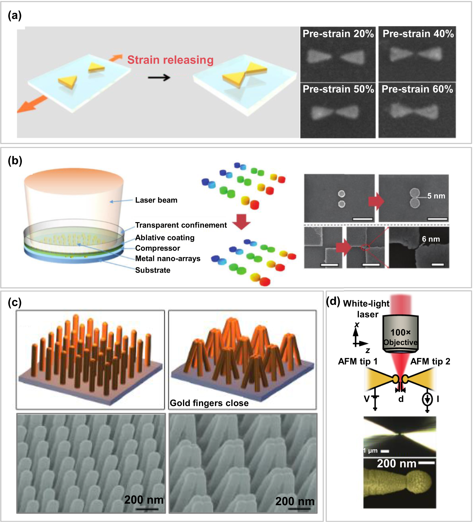
Standard image High-resolution image3.2.3. Post-assembling approaches.
In this part, we summarize the main post-assembling approaches that can effectively fabricate ultrasmall nanogaps down to the sub-10 nm scale by actively gathering prepatterned structures with mechanical approaches [155, 191]. Post-assembling steps yield gap size that are smaller than those directly fabricated by conventional lithography process. As depicted in figure 14(a) nanobowtie was first transferred on a pre-stretched elastomeric substrate, and two triangles with tip-to-tip arrangement moved closer to each other when the strain was released [192]. The gap size can be further shrunk to 5 nm. Cheng et al generated precise nanogaps with laser shock induced superplastic formation [193]. As shown in figure 14(b), prepatterned metal nanodimers were compressed, inducing lateral expansion with a high-deformation ratio. The gap size can be finely tuned by laser energy, and the realized gap can be as small as 5 nm. The cohesion of HAR structures stimulated by the capillary force in the meniscus during solvent drying is also used for nanogap fabrication [194, 195]. The gap size can be tuned by the thickness of coating layer on HAR structures. As shown in figure 14(c), arrayed gold nanofingers orderly cohere under the stimulus of a droplet of analyzer solvent, and the analyzer molecules absorbed on a gold surface form sub-nanometer gaps. Meanwhile, the analyzer molecules are placed in the gap of the plasmonic fingers [196]. The gap size is the thickness of the double molecular layers between the cohesive plasmonic fingers. In addition, actively tuning the nanogap size by approaching two metal-coated nanospheres at the free end of AFM tips was demonstrated by Savage et al [197], as seen in figure 14(d). The gap size can be finely tuned by electrostatic force. Sub-nanometer gaps that support the onset of quantum tunneling in a plasmonic cavity was demonstrated.

Figure 14. Post-assembling approaches for fabricating sub-10 nm gaps. (a) Stress-enabled narrowing gap in gold nanobowties on pre-stretched elastomers. (b) Ultrafine gap defined by the lateral expansion of a gold nanodimer utilized by laser shock induced superplastic formation. (c) Capillary force induced cohesion of gold nanofingers. (d) Active approaching of Au-coated nanospheres on AFM tips driven by electrostatic force. (a) Reprinted with permission from [192]. Copyright (2019) American Chemical Society. (b) [193]. John Wiley & Sons. © (2016) WILEY-VCH Verlag GmbH & Co. KGaA, Weinheim. (c) Reprinted with permission of [196]. Copyright (2010) American Chemical Society. (d) Reprinted by permission from Springer Nature Customer Service Centre GmbH: Springer Nature, Nature [197]. Copyright (2012) Nature Publishing Group, a division of Macmillan Publishers Limited. All Rights Reserved (2012).
Download figure:
Standard image High-resolution image3.3. Post-trimming approaches
Conducting sub-10 nm fabrication using a single method or technique is challenging under the simultaneous considerations of resolution and efficiency. Post-trimming for sub-10 nm fabrication is performed to define target features in additive and subtractive manners by combining two or more complementary methods.
3.3.1. Additive post-trimming.
Additive post-trimming is carried out to obtain higher resolution in features via material deposition. As shown in figure 15(a) local electrodeposition with self-inhibited reagent depletion was conducted on laterally disposed electrodes [198]. Lam et al also performed additive post-trimming with electrodeposition to shrink a separation between electrode pair from several tens of nanometers to the sub-10 nm scale [199]. However, interpenetrating jagged elements tend to form at the gap electrodes, limiting the process uniformity and reproducibility. The lateral growth that occurs in vacuum deposition can also be applied to perform controllable separation. As depicted in figure 15(b), vacuum evaporation was used to shrink the separation of clustered structures [200, 201]. The edge roughness of the resultant structure is better than that defined by electrodeposition. Hatzor and Weiss used a molecule ruler to scale down nanostructures [83]. As shown in figure 15(c), specific decoration of layer-by-layer mercaptoalkanoic acid molecules on gold surface can be performed to shrink the middle structure after pattern transfer. Post molecular trimming can produce a thinnest Pt line (<15 nm) the middle structure. Some other additive post-trimming examples include using ALD deposition to shrink the dimension of nanopores and nanoslits [202–204].

Figure 15. Additive post trimming approaches. (a) Electrodeposition-enabled narrowing of nanogaps between electrode pairs. (b) Lateral growth in evaporation to shrink nanogap size. (c) Molecular ruler for scaling nanostructures down to 10 nm. Scale bars: 200 nm. (a) Reprinted from [198], with the permission of AIP Publishing. (b) Reproduced from [201]. © IOP Publishing Ltd. All rights reserved. (c) From [83]. Reprinted with permission from AAAS.
Download figure:
Standard image High-resolution image3.3.2. Subtractive post-trimming.
Subtractive post-trimming is executed by the removal and consumption of materials in target structures to shrink the feature sizes. For sub-10 nm fabrication, atomically precise etching processes were carried out to reliably define nanogaps below 10 nm or sharp tip with sub-10 nm radius of curvature. As shown in figures 16(a) and (b), sub-10 nm gaps on patterned structures were fabricated by etching-based post trimming using 200 kV transmission FEB and He+-FIB [84, 127], respectively. Except for the removal of materials, the consumption of material with chemical reactions is another post-trimming approach. Si oxidization is a mature technique in semiconductor manufacturing, which has atomic precision for controlling the thickness of oxide layers. Walavalkar et al demonstrated the oxidization process for Si nanopillars and achieved a core Si nanowire with a diameter of 4 nm [205], as shown in figure 16(c). Self-assembled molecular nanopatterns were defined with the recognition of biotin-streptavidin through multiple subtractive micro-contact printing with nanoscale offsets in every step [206], as shown in figure 16(d). AFM images display the decreasing of feature sizes from 90 to 15 nm. The main challenge of this method is the actuation precision of overlay in multiple PDMS contact microprinting. Subtractive post-trimming has also shown a particular capability of fine tuning the sharpness of nanotips for imaging or nanofabrication either via electrochemical or FIB processes [75, 207].

Figure 16. Subtractive post trimming approaches. (a) Electron-beam sculpting for single-nanometer gap fabrication. (b) He+-FIB milling to etch sub-10 nm gap in gold nanorods. (c) Oxidization of Si nanopillars to prepare sub-10 nm nanowires. (d) Multiple nanometric offset micro-contact printing to fabricate molecular patterns with feature sizes of ∼10 nm. (a) Reprinted with permission from [127]. Copyright (2005) American Chemical Society. (b) Reprinted with permission from [84]. Copyright (2013) American Chemical Society. (c) Reprinted with permission from [205]. Copyright (2010) American Chemical Society. (d) From [206]. Reprinted with permission from AAAS.
Download figure:
Standard image High-resolution image4. Applications
As an enabling platform, sub-10 nm fabrication has enabled various high-performance and new-concept devices. In these devices, high-performing CMOS manufacturing is the most attractive application of sub-10 nm fabrication. However, considering that the realization of sub-10 nm resolution in CMOS devices involves a sophisticated process portfolio and has been well documented by many researchers, we collected only representative non-CMOS applications that have the capability of sub-10 nm fabrication in this section.
4.1. Plasmonic nanogaps enhanced spectroscopy
Plasmonic nanogaps are a promising platform for surface-enhanced spectroscopy, such as surface enhanced Raman scattering (SERS) [209–212, 241], surface enhanced infrared absorption (SEIRA) [213–215, 242], surface enhanced fluorescence (SEF), and enhanced nonlinear optics [216–219] because of large near-field enhancement. The enhancement factor strongly depends on gap size at the sub-10 nm scale. Huck et al used a single gold nanorod dimer to demonstrate the dependance of SEIRA performance with respect to gap size (figure 17(a)) [215]. In their work, the enhancement factor enabled by a 3 nm gap was one order of magnitude higher than that of a 50 nm gap. Therefore, the reliable fabrication of sub-10 nm plasmonic gap is the key to high-performance surface enhanced spectroscopy. In order to reliably fabricate sub-10 nm plasmonic nanogaps, Duan et al developed a metal lift-off method based on high-resolution electron-beam lithography using HSQ resist [208], as shown in figure 17(b). Densely distributed nanotriangles presented an 11 times higher enhancement factor than that enabled by nanodisks. Semiconductors are also a promising material for plasmonics, due to its simple structure based on mature nanofabrication technologies and low optical loss. Regmi et al reported that a Si nanodisk dimer with a nanogap has a SEF capability at the single molecule level [219], as shown in figure 17(c). In their work, the performance was improved by a factor of 270. Large near-field enhancement in sub-10 nm plasmonic gaps can greatly amplify the weak nonlinear-optics phenomenon. Metzger et al significantly enhanced the third harmonic generation (THG) nonlinear optical performance of indium tin oxide (ITO) nanocrystal, a high THG-efficiency material, which was placed in the gap of a gold rod dimer (see figure 17(d)) [220]. The gold rod dimers hybridized with ITO nanocrystals in the nanogap emit twice as much THG compared to the bare gold rod dimer.

Figure 17. Typical surface-enhanced spectroscopic applications based on plasmonic nanogaps. (a) SEIRA to detect single 4,4'-bis(N-carbazolyl)-1,1'-biphenyl molecule using plasmonic nanorod dimers with nanometric gaps. (b) Densely distributed gold nanostructure array with 10 nm gaps for SERS application. The SEM image is the low-magnification view of densely distributed gold nanodisks with 10 nm gaps. The right diagram shows the SERS signal from different shaped densely distributed nanostructures. Scale bar: 200 nm. (c) All-dielectric Si nanogap enhanced fluorescence for molecular detection. The left panel shows the schematic of SEF configuration based on a single Si nanodimer with a nanogap. The right panel presents the SEM image of a single Si nanodimer with a gap size of 20 nm. (d) Schematic of enhanced THG by the hybrid ITO nanocrystal-incorporated plasmonic gap-antenna. (a) Reprinted with permission from [215]. Copyright (2014) American Chemical Society. (b) Reprinted with permission from [208]. Copyright (2011) American Chemical Society. (c) Reprinted with permission from [219]. Copyright (2016) American Chemical Society. (d) Reprinted with permission from [220]. Copyright (2014) American Chemical Society.
Download figure:
Standard image High-resolution image4.2. Nanogap electrodes
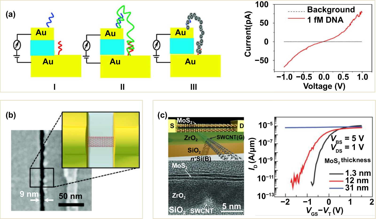
Nanogap electrodes are not only the building blocks of high-performance nanoelectronic devices but also a platform to achieve high-sensitivity sensing based on conductance transition for trace detection [221, 226–228]. Roy et al performed DNA detection with 1 fM level based on electrochemical sensing using a nanogap electrodes array [221]. A nanogap electrode is a pair of top and bottom Au electrodes that are separated by a nanometer-thick SiO2 layer. The gap size in electrodes can be easily tuned in the range of 5–20 nm by changing the thickness of the SiO2 layer. Two DNA capture probes were immobilized to both electrodes. A primary current pathway was created by hybridizing two termini of the target DNA with capture probes on electrodes. The signal in conductance was then detected, as shown in figure 18(a).

Figure 18. Typical applications of nanogaps electrodes. (a) Schematic of the nano-metal/insulator/metal multilayer sensor device and representative I–V curve for a 1.0 fM target DNA as referred to as 'background.' (b) Top-view SEM image of a 9 nm channel CNT transistor. (c) Schematic of a 1D2D-FET with an MoS2 channel and SWCNT gate. Cross-sectional TEM image of a representative sample showing the SWCNT gate, ZrO2 gate dielectric, and bilayer MoS2 channel. Dependence of MoS2 channel thickness on the performance of 1D2D-FET. (a) Reprinted with permission from [221]. Copyright (2009) American Chemical Society. (b) Reprinted with permission from [170]. Copyright (2012) American Chemical Society. (c) From [222]. Reprinted with permission from AAAS.
Download figure:
Standard image High-resolution imageScaling down the channel length to the sub-10 nm scale is an effective approach to build ultrafast and high-performance transistors. However, the definition of sub-10 nm gap electrodes is a long-standing challenge. To achieve this goal, much meaningful work on sub-10 nm channel transistors has been conducted. IBM researchers fabricated a 9 nm channel carbon nanotube (CNT) transistor using edge lithography [170], as shown in figure 18(b). In combination with an optimized W gate, 3 nm thickness HfO2 gate oxide and palladium (Pd) source/drain contacts, the fabricated CNT transistor exhibited a considerably improved subthreshold slope. Furthermore, Javey et al applied SWCNT as a gate to achieve a 1 nm channel MoS2 transistor [222]. The transistor with such a short channel exhibited that the controllability of output characteristics is strongly dependent upon the gate oxide thickness. At the scaling limit of the gate length, the gate oxide thickness must also be scaled down accordingly, as shown in figure 18(c).
4.3. Nanotip for field emission sources
A field emission source can produce a focused spot with an ultrasmall radius, which is a key component for high-end facilities for characterization (e.g. electron microscopic series and high-energy spectroscopic series) and fabrication (e.g. EBL and FIB) in nanoscience. Induced by a strong electrostatic field, a high field gradient is generated near the apex of the tip, which enables electrons to spill out from the cathode to the vacuum and promotes the ionization of gas molecules around the apex. A sharper tip can generate higher field gradients and reduce operation voltage. Therefore, sub-10 nm tip emitters are of great importance in high-resolution microscopic imaging and fabrication. For example, in photoemission electron microscopy (PEEM)—a type of electron microscopy that applies the local variation of electron emission induced by light, the spatial resolution is mainly determined by the quasi-point-like electron emitter enabled by the ultrasharp tip [223, 224]. Figure 19(a) shows an experimental setup scheme for a time-resolved photoemission electron microscope. The sharp gold nanotaper provides a compact source of ultrashort electron pulses with ultrahigh time resolution [224]. A single metallic tip with ∼20 nm radius emits intense multiphoton femtosecond electron emission pulses. Field ion emission is also based on the sharp metal tip. Kuo et al reported a thermally stable Ir/W(111) single-atom tip that can emit high-brightness inert gas (e.g. He+, Ar+) and reactive gas (e.g. H+ 2, O+ 2) ion beams with high current stability (figure 19(b)) [229]. As shown in figure 19(c), the helium ion emitter in the He+-FIB system is a trimmer configuration of three W atoms at the apex of the hairpin filament [230]. The atomic scale tip makes single ion emission possible from the end of the emitter and provides a promising platform for atom-scale fabrication, such as nanopores for DNA sequencing and quantum light source-based nitrogen vacancy (NV) centers, as discussed in later parts.

Figure 19. Field emission applications based on nanotips. (a) Schematic setup of time resolved PEEM and electron emission distribution at the apex of the tip. (b) Experimental setup scheme of the gas-field ion source. (c) Image of the helium ion source, which is the trimmer configuration of three tungsten atoms at the apex of the filament. (a) Reprinted with permission from [224]. Copyright (2015) by the American Physical Society. (b) Reprinted from [229], with the permission of AIP Publishing. (c) Reprinted with permission from [230]. Copyright (2006) American Vacuum Society.
Download figure:
Standard image High-resolution image4.4. Nanopores for genetic sequencing
Nanopore-based devices are significant to next-generation genetic sequencing because they possess the potential to quickly and reliably sequence genetic information at low cost. As shown in figure 20(a), the basic concept involve monitoring the change of ion current blockade when unzipped DNA strands translocate through the nanopore [41]. The ion current varies due to the delicate different sizes of the four bases (i.e. A, G, C, T). Obtaining nanopores of comparable size to DNA strands (∼2 nm) is the prerequisite for sequencing accuracy. Originally, biological transmembrane proteins inserted in a lipid bilayer served as nanopores. This sort of biological nanopore is well defined and highly reproducible in size and structure. Nevertheless, constant nanopore size and the instability of fragile lipid bilayer structures limit the biological nanopore in practical applications. Hence, solid-state nanopores perforated on inorganic membranes have attracted much attention due to their robustness, geometry control, and surface properties. Compared to biological nanopores, the preparation of solid-state nanopores is supposed to eventually be compatible with mature semiconductor fabrication technologies. In 2001, Golovchenko et al demonstrated a 1.8 nm pore in a SiNx membrane using an 'ion-beam sculpting' method and realized DNA detection [202]. In later decades, extensive studies on the fabrication of solid-state nanopores (e.g. TEM sculpting, He+-FIB milling, and controlled dielectric breakdown) have been exhibited [231]. However, the limited fabrication accuracy in size has inhibited the further improvement of the sequencing capability via merely monitoring ion current blockade. To address this issue, synchronous detection of both the ion current blockade signals and other in-sync detection signals, is regarded as an alternative to enhance the accuracy of sequencing and detection. For example, electronic sensing using electrodes [231, 232] (see figures 20(b) and (c)) and spectroscopic amplification based on plasmonic antennas [233, 234] (see figures 20(d) and (e)) were used for synchronous analysis. These nanopore-based devices require additional lateral sub-10 nm fabrication and overlay accuracy. In addition, considering the fabrication feasibility, lateral nanochannels have recently been investigated as an alternative platform for DNA sequencing [77].
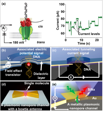
Figure 20. Nanopore-based DNA sequencing technologies. (a) Basic concept of DNA sequence using a nanopore. (b) Schematic of nanopore sequencing associated with the analysis of electrical potential signals enabled by nanogap electrodes. (c) In-sync tunneling current from a lateral nanogap electrode as a complementary signal to enhance the sequencing accuracy. (d) Sub-10 nm pores device on SiNx membranes for molecular detection. (e) Sub-10 nm Au nanopore device integrated into an electrochemical system. (a) Reprinted by permission from Springer Nature Customer Service Centre GmbH: Nature Biotechnology, Nature Biotechnology [41]. Copyright (2016) Nature Publishing Group, a division of Macmillan Publishers Limited. All Rights Reserved (2016). (b) Reused with permission from [232] of Nokia Corporation and AT&T Archives. (c) Reprinted by permission from Springer Nature Customer Service Centre GmbH: Springer Nature, Nature Nanotechnology [233]. Copyright (1969) Nature Publishing Group (1969). (d) Reprinted with permission from [234]. Copyright (2014) American Chemical Society. (e) [235]. John Wiley & Sons. © 2016 WILEY-VCH Verlag GmbH & Co. KGaA, Weinheim.
Download figure:
Standard image High-resolution image4.5. Quantum devices
Sub-10 nm nanofabrication is fundamentally important for developing quantum devices because the structures and features at the single-nanometer scale and even atomic scale are capable of promoting quantum effects.
4.5.1. Tunneling devices.
As the separation size between two conductors decreases to a sufficiently small distance, the electrons in one conductor can pass through barriers and generate the tunneling effect. Based on the tunneling effect, tunneling devices (e.g. SET) and tools (e.g. STM) have been demonstrated in recent decades [235, 236]. In tunneling devices, reliable fabrication of small gaps with single-digit nanometers is crucial. Goldhaber-Gordon et al reported an SET device which consists of three gate electrodes and one collector electrode, as shown in figure 21(a) [237]. To obtain nanometer gap and island size, this SET was fabricated by electron-beam lithography, which was critical to observe the Kondo effect. Schoelkopf et al demonstrated an electrometer based on the configuration of SET [238]. The electrometer was fabricated by an EBL-defined suspended resist bridge and a double-angle evaporation method, which allowed the study of single electron tunneling oscillations, as shown in the SEM image of figure 21(b). The direct-current conductance displayed Coulomb blockade oscillations, and the reflected carrier power was strongly correlated with the transistor's conductance. Ultrasmall gaps can also be used to the realize high-temperature superconductive (HTS) hybrid devices. Baghdadi et al fabricated a 35 nm YBa2Cu3O7−δ (YBCO) encapsulated nanogap defined by a conformally deposited film thickness [239], as shown in figure 21(c). Such a small superconducting YBCO nanogap bridged with a conventional metal induced a proximity Josephson coupling. Very recently, researchers performed stable plasmon-induced tunneling in particle-on-film configurations, in which the nanogaps were defined by an ultrathin ALD-coated dielectric layer [240], as shown in figure 21(d). The device consisted of a vacuum tube with an optically excited emitter or photocathode, similar to a microscale phototube, which is supposed to have potential applications in carrier-envelope phase photodetectors.

Figure 21. Typical applications of tunneling devices. (a) SEM image showing the top view of an SET device. (b) SEM image of the radio-frequency single-elelcton transistor (RF-SET) devices and the relationship between gate voltage and conductance. (c) SEM image of the final YBCO-based HTS hybrid device. (d) Sketch of an example device and experimental arrangement. Optical microscope image of an emitter array and SEM image of plasmonic nanotriangle and nanorod arrays. (a) [237] (1998) © Springer Science + Business Media Dordrecht 2001. With permission of Springer. (b) From [238]. Reprinted with permission from AAAS. (c) Reprinted figure with permission from [239]. Copyright (2015) by the American Physical Society. (d) Reprinted by permission from Springer Nature Customer Service Centre GmbH: Springer Nature, Nature Physics [240]. Copyright (2016) Nature Publishing Group, (2016).
Download figure:
Standard image High-resolution image4.5.2. Quantum devices based on the confinement effect.
Quantum confinement is promoted when the size of a material is comparable to the de Broglie wavelength of electron wave function, which can enable energy band engineering of electrons in various applications. The most well-known examples are semiconductor quantum dots and gold nanocrystals for luminescence, which have already been widely used in industry. The NV center is another important example, which is regarded as a promising candidate for quantum light sources in integrated photonics because of its ease of fabrication and integration compatibility with waveguides. Hausmann et al demonstrated single NV centers hosted in suspended diamond photonic crystal cavities with quality factors up to 6000, as shown in figure 22(a) [244]. The emission property of the NV center can be tuned by its size. Electron band engineering can also enhance the performance of catalysts by tuning their dimensions and introducing non-noble metal to form alloys. For instance, Chen et al demonstrated alloy nanocrystal libraries via pyrolysis of metalorganic precursor nanopatterns defined by SPL [245], as shown in figure 22(b). Using polymer nanoreactor-mediated synthesis, a quinary alloy nanocrystal (∼30 nm) can be prepared with five metallic elements (Au, Ag, Co, Cu and Ni), which has the potential to obtain multimetallic nanoparticles toward higher compositional diversity and structural complexity for catalysis. The electronic properties can be engineered via quantum confinement, a famous example of this effect is graphene. Graphene is a promising electronic material due to its extremely high mobility. Zero bandgap limits its application in transistor devices, but non-zero bandgap can form in graphene nanoribbons. The bandgap increases for smaller nanoribbons. Dai et al reported that sub-10 nm graphene nanoribbons with smooth edges can act as semiconductors. Furthermore, they applied a sub-10 nm graphene nanoribbon with adequate bandgap to fabricate FETs which could be operated at room temperature [246], as shown in figure 22(c). More interestingly, quantum confinement has the potential to convert indirect bandgap semiconductors to direct bandgap semiconductors for luminescence applications. To this end, Si nanocrystals have been extensively investigated. For example, Valenta et al prepared Si quantum dots using two-stage oxidization of regular Si nanopillars which were fabricated by EBL and plasma etching, as shown in figure 22(d) [247]. The photoluminescence spectroscopy can be detected at room temperature.

Figure 22. Typical applications based on the quantum confinement effect. (a) Schematic diagram of an integrated quantum light source based on an NV center in photonic crystal cavities. (b) Fabrication scheme of multicomponent alloy nanoparticles with the pyrolysis of a printed metalorganic precursor mixture by DPN. The right graphs show the energy dispersion spectroscopy mappings and TEM micrograph of different elements in a single trinary alloy nanocrystal. (c) Schematics of graphene-nanoribbon FET device and AFM topography mappings of different-width graphene channel sections. (d) SEM images (45° tilt view) of Si quantum dots after initial patterning and size-trimming by the first oxidation step and corresponding PL spectra on an Si core with a varied diameter. (a) Reprinted with permission from [244]. Copyright (2013) American Chemical Society. (b) From [245]. Reprinted with permission from AAAS. (c) Reprinted figure with permission from [246]. Copyright (2008) by the American Physical Society. (d) Reprinted from [247]. Copyright (2002) with permission from Elsevier.
Download figure:
Standard image High-resolution image
5. Conclusions and outlooks
This review covered the existing techniques and methods for fabricating structures with sub-10 nm features, and summarized the main applications enabled by these sub-10 nm features and driven by both the further miniaturization of devices and critical-size-dependent new-concept nanodevices. Continuously pushing the nanofabrication capability to the sub-10 nm scale is not only a demand of the IC industry, but also highly desirable for the research and development of nanoelectronic, nano-optical, biomedical, and quantum devices. Meanwhile, sub-10 nm fabrication provides a technological platform for creating artificial materials and metadevices to explore new physical phenomena and effects that only appear at such a small scale. With decades of efforts, researchers have developed a large number of methods to obtain structures with sub-10 nm features via either lithographic or unconventional approaches. With these sub-10 nm fabrication capabilities, various high-performance and new-concept device applications have been demonstrated and several new phenomena have been explored. Though significant progress has been made in the past decades, there are still many limitations and challenges for this research area. From the resolution point of view, further pushing the resolution down to the 1 nm scale and even the atomic scale is still challenging. From the perspective of practical applications, only a few of these collected fabrication techniques and methods, such as EUV and nanoimprinting, can be adopted in high-volume manufacturing. Considering the reliability, accuracy, fabrication efficiency, and cost, most of them can only be applied for proof-of-concept demonstrations in laboratory settings. In addition, the existing fabrication techniques are only available for defining planar structures, which cannot satisfy 3D fabrication requirements.
Considering it is not realistic to apply EUV for non-IC applications due to its high facility and process costs and the material/process incompatibility, developing reliable sub-10 nm fabrication techniques with higher resolution and lower cost over large areas is still an essential demand for nanoscience and nanotechnology. This requirement calls for the combination of efforts, including further improving the performance of fabrication tools, developing more advanced process portfolios, and using better materials, such as new resists. To further push the resolution to atomic scale, the fabrication techniques based on single atoms and molecules, such as single ion implantation, atomic layer deposition, atomic layer etching, and single heavy ion lithography, should be extensively explored. Meanwhile, understanding the nanoscale and atomistic mechanics, thermodynamics and kinetics during the processes will become particularly significant for realizing atomistic control of fabrication, which requires more efforts on methods and molecular-dynamic techniques for simulations.
Regarding the applications at the sub-10 nm scale, other than the driving force from the IC industry, numerous devices for single electrons, single photons, and single molecules have also been demonstrated. These new-concept devices are supposed to support next-generation technologies based on quantum mechanics. However, most of these devices are limited by the current fabrication capability and remain in the laboratory and far from the commercialization. It is believed that the development of these devices could be accelerated along with the availability of the nanofabrication techniques at the 1 nm and atomic scales. Considering the compatibility of the materials and processes in device fabrication, merely using lithographic methods to achieve such high resolution becomes increasingly difficult, and the combination of bottom-up growth and assembly with top-down lithography techniques is expected to be a feasible strategy in future 1 nm and atomic-scale device fabrication.
Acknowledgments
This work is supported by the National Natural Science Foundation of China (Grants Nos. 51722503, 51805160 and U1930114), the National Key Research and Development Program of China (Grant No. 2018YFE0109200), and the Guangdong Basic Research Foundation (Grant No. 2020A1515110971).