
Abstract
In this study, the photovoltaic behavior of centimeter-long lateral organic junctions, reaching 1.8 cm, is reported. The organic junctions are formed using organic semiconductor films with high mobilities of holes and electrons. The lateral diffusion lengths of photogenerated electrons and holes are 4.7 and 5.5 mm, respectively. The photovoltaic behavior in the centimeter-long lateral junctions is controlled by the trap-assisted recombination between the electrons and holes.
Export citation and abstract BibTeX RIS

Content from this work may be used under the terms of the Creative Commons Attribution 4.0 license. Any further distribution of this work must maintain attribution to the author(s) and the title of the work, journal citation and DOI.
Organic semiconductors with high carrier mobilities up to 40 cm2 V−1·s−1 have been reported. 1–4) Such high mobilities were observed for carriers moving laterally through the material because of π–π stacking parallel to the organic crystal surface.
The limitations owing to vertical transport of carriers 5–7) and vertical thickness in conventional sandwich-type organic photovoltaic cells 8–11) can be controlled by lateral transport and collection of photogenerated carriers. 12,13) Therefore, lateral-type organic photovoltaic cells using high-mobility organic semiconductors, such as single crystals 12,14) and crystalline films, 13) have been studied. However, the factors required to achieve macroscopically wide lateral junctions are unknown. In this study, the dependence of photovoltaic properties on the macroscopic lengths of the lateral junctions in 2,7-dioctyl[1]benzothieno[3,2-b][1]benzothiophene (C8-BTBT) [Fig. 1(a)] and N,N'-dioctyl-3,4,9,10-perylenedicarboximide (PTCDI-C8) [Fig. 1(a)] films are analyzed. The hole mobility of C8-BTBT is 43 cm2 V−1 s−1, 15,16) and the electron mobility of PTCDI-C8 is 1.7 cm2 V−1 s−1. 17)
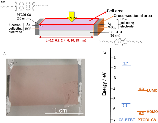
Fig. 1. (Color online) (a) Structure of a lateral junction cell. (b) Photograph of a lateral cell (L = 18 mm). (c) Energy diagram of C8-BTBT and PTCDI-C8.
Download figure:
Standard image High-resolution imageFigure 1 shows the structure of a lateral junction cell. The films C8-BTBT (Nippon Kayaku Co., Ltd.) and PTCDI-C8 (Luminescence Technology) were used as the donor and acceptor, respectively. The organic semiconductors were placed in an oil-free vacuum chamber, which was housed in a glove box (EpiTech Inc., 12ET12007), under 10−6 Pa pressure at room temperature. The evaporation rate and thickness of the C8-BTBT and PTCDI-C8 films were 0.1 nm s−1 and 50 nm, respectively. The C8-BTBT and PTCDI-C8 films were sandwiched between 100 nm thick Ag electrodes through a 10 nm thick MoO3 and 10 nm thick bathocuproine (BCP) on either sides using a customized movable mask system (EpiTech Inc.) [Fig. S1(a) available online at stacks.iop.org/APEX/14/094001/mmedia]. BCP/Ag and MoO3/Ag acted as the electron- and hole-collecting electrodes, respectively [Fig. S1(b)]. The distance (L) between the electron-collecting electrode (BCP/Ag) and hole-collecting electrode (MoO3/Ag) varied between 0.2 and 18 mm. A photograph of the cell with L = 18 mm is shown in Fig. 1(b), and the energy diagram of C8-BTBT and PTCDI is shown in Fig. 1(c). 18)
The current–voltage (J–V) characteristics were measured under simulated solar light irradiation (AM1, 100 mW cm−2, ASAHI Spectra, HAL-320) and N2 atmosphere. The intensity of simulated solar light was varied from 0.1 to 10 sun using a neutral density filter.
Figure 2(a) shows the J–V characteristics of the cells [Fig. 1(a)] with L = 0.2, 0.7, 2, and 18 mm. The vertical axis corresponds to the short-circuit photocurrent density per cell area [Jsc/μA cm−2, Fig. 1(a), red rectangle]. Remarkable photovoltaic characteristics were observed for all cells [Fig. 2(a)]. Even a lateral cell with L = 18 mm [Fig. 2(a), red curve] exhibited prominent photovoltaic behavior. The Jsc steeply decreased from 4 (L = 0.2 mm) to 0.015 μA cm−2 (L = 18 mm) [Fig. 2(b)], and the open-circuit photovoltage (Voc) gradually decreased from 0.79 (L = 0.2 mm) to 0.42 V (L = 18 mm) [Fig. 2(c)]. Moreover, the fill factor (FF) decreased from 0.56 (L = 0.2 mm) to 0.32 (L = 18 mm) [Fig. 2(d)]. The photovoltaic behavior of centimeter-long lateral organic junctions was observed even in less photocurrent.
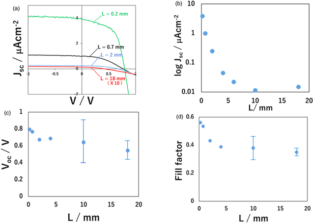
Fig. 2. (Color online) (a) Jsc–V characteristics of cells with L = 0.2 (green curve), 0.7 (black curve), 2 (blue curve), and 18 mm (red curve). Dependence of (b) Jsc, (c) Voc, and (d) FF on L. Simulated solar light of 100 mW cm−2 was irradiated.
Download figure:
Standard image High-resolution imageTo understand the mechanism of photocarrier generation in the centimeter-long lateral junctions, the dependence of J–V characteristics on the light intensity was studied [Fig. 3(a)]. The photocurrent density increased with an increase in the light intensity. Striking J–V curves were observed even under 10 sun irradiations at L = 2 mm, despite the presence of the resistive effect. At L = 2 mm, a slope of 0.95 was obtained, which interpreted the relationship between the Jsc and light intensity [Fig. 3(b)]. Figure 3(c) shows the dependence of the slope of the light intensity plots in Fig. 3(b) on L. At an infinitesimal L (0.2 mm), the slope approached unity (0.99), and when L increased from 2 to 18 mm, a slight decrease in the slope values was observed with a value of 0.90 at 18 mm. These results indicate the absence of bimolecular recombination at L = 0.2 mm and the minimal effect of bimolecular recombination between the holes in C8-BTBT film and electrons in PTCDI-C8 film 19) when L was varied from 2 to 18 mm. Minimal bimolecular recombination occurred in the lateral cell even at L = 18 mm.
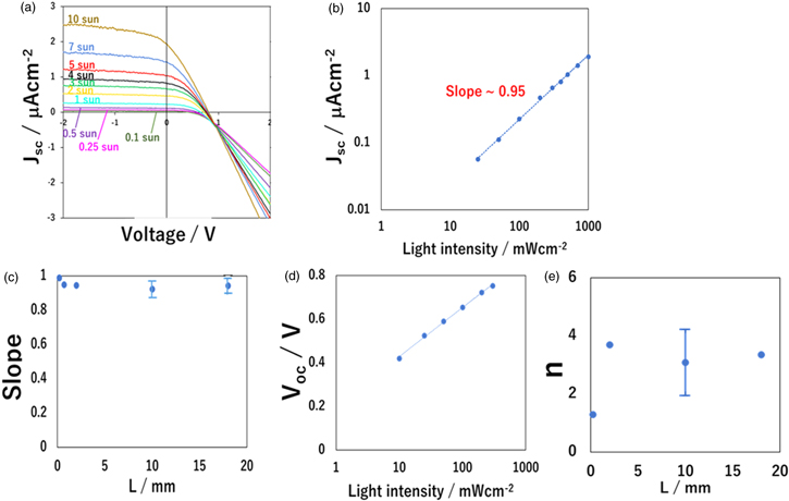
Fig. 3. (Color online) (a) Jsc–V characteristics of cells with L = 2 mm under irradiation at various intensities of simulated solar light from 0.1 to 10 sun. (b) Logarithmic plot between Jsc and light intensity. (c) Dependence of the slopes obtained from the light intensity plots in Fig. 3(b) on L. (d) Semi-logarithmic plot between Voc and light intensity. Solid line is the least-squares fitting. (e) Dependence of n obtained from the slope of the line in Fig. 3(d) on L.
Download figure:
Standard image High-resolution imageA linear relationship was observed in the semi-logarithmic plot between the Voc and light intensity, as shown in Fig. 3(d). The slope was expressed as nkT, 20–22) where n, k, and T, were the diode factor, Boltzmann constant, and absolute temperature, respectively. The diode factor, n, could be determined from the slope in the figure. In ideal p–n junctions, n is equal to unity, and n greater than unity indicates the presence of trap-assisted recombination. 23,24) Thus, minimal trap-assisted recombination was observed at L = 0.2 mm, and significant trap-assisted recombination occurred when L was varied from 2 to 18 mm [Fig. 3(e)]. Although the value of n normally ranges between 1 and 2, an n value greater than 2 was reported when the quality of diode was substandard. 25)
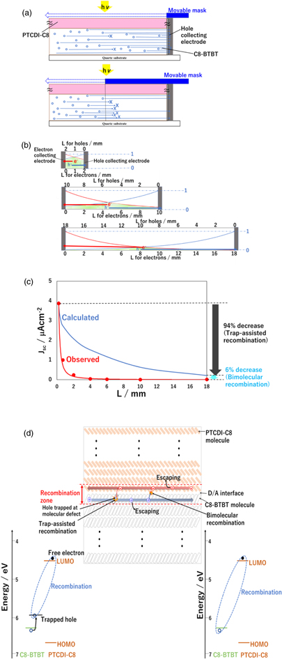
To analyze the performance of lateral cell due to the photogenerated electrons and holes, movable-mask experiments were performed [Fig. 4]. For holes, the movable mask was introduced between the cell surface and irradiated light, and it glided from the hole-collecting electrode to the electron-collecting electrode [Fig. 4, upper]. For electrons, the movable mask was glided in the opposite direction [Fig. 4, lower]. Figure 4 (middle) shows the semi-logarithmic plots of Jsc against the mask-edge distance from the hole-collecting electrode (x) (blue dots) for cells with L = 4, 6, and 18 mm. A gradual decrease in Jsc was observed as the mask moved towards the electron-collecting electrode. Moreover, the observed values of Jsc exponentially dropped with an increase in distance. The hole diffusion length (Lh) was obtained from the plot of photocurrent density, (1/e) Jsc (L = 0 mm), against L, as shown in Fig. S2. The hole diffusion lengths (Lh) for L = 4, 6, and 18 mm were 5.3, 6.3, and 4.8 mm, respectively, as determined from the slopes of the fit, and the average Lh was 5.5 mm. Furthermore, Fig. 4 (middle) shows the semi-logarithmic plots of Jsc against the mask edge distance from the electron-collecting electrode (y) (red dots) for cells with L = 4, 6, and 18 mm. The electron diffusion length (Le) was 4.7 mm. The Le (4.7 mm) and Lh (5.5 mm) values were macroscopic and large.
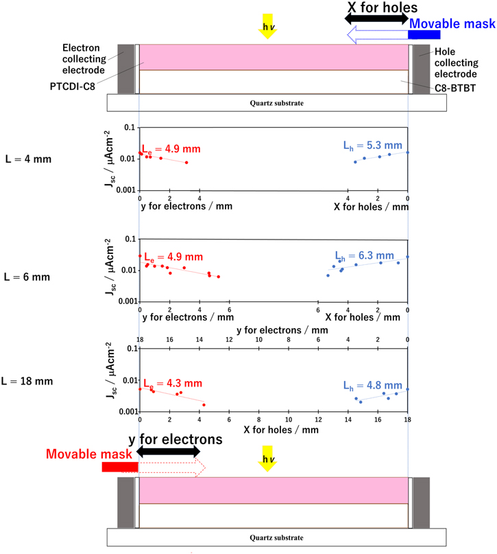
Fig. 4. (Color online) Schematic diagram of movable-mask experiments for holes (upper) and electrons (lower). Semi-logarithmic plots (middle) between Jsc and mask edge distance from hole-collecting electrode (x) (blue dots, right side) and electron-collecting electrode (y) (red dots, left side) for cells with L = 4, 6, and 18 mm.
Download figure:
Standard image High-resolution imageFigure 5(a) shows the schematic of the hole movement with (lower) and without (upper) a movable mask. Without the movable mask, most of the holes photogenerated near the hole-collecting electrode were collected. With the movable mask (lower), most of the holes photogenerated away from the hole-collecting electrode were not collected, that is, the holes were captured in the traps. Hence, the observation with the movable mask revealed that Le and Lh are prominently due to the trapping of electrons and holes, respectively. The trapping is directly associated with the trap-assisted recombination, as shown in Fig. 5(d).
Fig. 5. (Color online) (a) Schematic diagram of hole movement with (lower) and without (upper) movable mask. (b) Profiles of the portion of electrons (red curves) and holes (blue curves) collected by the electron-collecting and hole-collecting electrodes. Only the carriers in the green-shaded region contribute to the photocurrent. (c) Dependence of Jsc on L. The calculated and observed Jsc values are represented by the blue and red curves, respectively. (d) Schematic illustration of recombination zone at donor (D; C8-BTBT)/acceptor (A; PTCDI-C8) interface in the double layer of C8-BTBT (50 nm) and PTCDI-C8 (50 nm).
Download figure:
Standard image High-resolution image
Figure 5(b) shows the profiles of the portion of electrons (red curves) and holes (blue curves), which were collected by the electron-collecting and hole-collecting electrodes. The profiles exponentially decrease with increasing distance. The red and blue curves are plotted using the average Le (4.7 mm) and Lh (5.5 mm), respectively. Electron and hole mobilities measured by field-effect transistor for vacuum evaporated films of PTCDI-C8 and C8-BTBT are reported 1.7 17) and 2.3 cm2 V−1 s−1. 15) Similar mobility values for electrons and holes seems to be the reason of similar diffusion lengths observed in this study. To generate photocurrent, the photogenerated electrons and holes should be extracted by the respective electrodes, which indicates that only the photogenerated carriers depicted in the green-shaded region contribute to the generation of photocurrent. Figure 5(c) shows the dependence of Jsc on L. The blue curve denotes the calculated Jsc from the green-shaded region. We calculated the whole area of the green shaded regions in Fig. 5(b) by adding the current densities of the tiny divided regions of 0.1 mm intervals. The red curve shows the observed Jsc. The considerable decrease in photocurrent is attributed to the trap-assisted recombination indicated by the blue curve. This decrease is calculated from the Le and Lh dominated by the traps [Fig. 5(a)]. The calculated and observed Jsc must be equal in an extremely small L (<0.4 mm) region for the two curves in this region to be adjusted owing to the absence of bimolecular recombination. A difference was observed between the calculated (blue) and observed (red) curves owing to an additional recombination in the regions with large L. It was concluded that this process was bimolecular recombination since the slope of the light-intensity dependent line [Fig. 3(c)] was significantly lesser than unity (0.90) for L > 2 mm. At L = 18 mm, the percentage of the trap-assisted [Fig. 5(d)] and bimolecular [Fig. 5(d)] recombinations were 94 and 6%, respectively.
Figure 5(d) shows the schematic illustration of donor (D; C8-BTBT)/acceptor (A; PTCDI-C8) interface. We assume the recombination occurs between the neighboring C8-BTBT/PTCDI-C8 molecules at the D/A interface as discussed in Fig. S3. Bimolecular recombination occurs between this C8-BTBT/PTCDI-C8 molecular pair. Trap-assisted recombination [Fig. 5(d)] occurs between electron in PTCDI-C8 and hole captured at the defect site of C8-BTBT acting as a trap such as molecular vacancy. Electrons and holes which are not captured by the traps can escape the recombination zone by moving the vertical direction of the film.
Based on this model, both bimolecular and trap-assisted recombination increases with increasing the encounter length between holes and electrons, i.e. electrode distance (L). Simultaneously, escaping probability of electrons and holes which are not captured by traps increases with increasing electrode distance (L). Former corresponds to the increase of the ratio of bimolecular recombination from 0.2 to 0.7 mm [Fig. S3(c)] and continuing increase of the ratio of trap-assisted recombination from 0.2 to 18 mm [Fig. S3(d)]. Latter corresponds to the gradual decrease of the ratio of bimolecular recombination above 0.7 mm. It should be noted that above L = 0.7 mm, at which the carrier escaping effect was appeared, roughly coincides with the end point of decreasing of slope of light intensity dependence [Fig. 3(c)]. Namely, probability of bimolecular recombination becomes constant due to the escape of holes and electrons from recombination zone [Fig. 5(d)]. If the traps are formed at molecular defects, such as molecular vacancy or dislocation, the lateral junction length can be further increased by removing the defects.
In conclusion, the photovoltaic behavior of centimeter-long organic lateral junctions was studied. This was accomplished by the large diffusion length for holes (5.5 mm) and electrons (4.7 mm). In long lateral cells, the trap-assisted recombination controlled the magnitude of the photocurrent density. The magnitude of photocurrent is small in this study; however, the application of advanced technology in organic film fabrication may yield a significant photocurrent output (Fig. S5). The centimeter-long carrier diffusions can overcome the limitation of route formation in the blended junctions in organic photovoltaic cells. 13) Application to the position sensitive detector 26,27) might be expected because of the photosensitive large area of the present device [Fig. 1(b)].
Acknowledgments
We acknowledge the funding from JSPS KAKENHI (No. 17K19110). Further, we appreciate the internship program between Chimie ParisTech and IMS.