1. Introduction
An RF transceiver integrated circuit operating in the MedRadio band is widely employed for biomedical devices and sensors, as the wireless communication is essentially needed between the implanted or body-worn medical devices and outside controllers. The wireless connectivity for the biomedical devices is used to exchange the diagnostic and therapeutic data. Its non-invasiveness significantly improves the patient’s comfortability by avoiding unnecessary painful surgical operations. The MedRadio band was assigned in 2009 [
1], in the frequency band of 401–406 MHz providing a total 5 MHz of contiguous spectrum on a secondary and non-interference basis. The MedRadio rule was amended later in 2011 to allow networking of the devices and controllers and referred to as a medical micropower network (MMN) [
2]. Since then, numerous implanted and wearable medical devices equipped with the MedRadio RF transceiver have been reported in literature, such as a wireless bio-signal monitoring system [
3], an implanted cardiac defibrillator [
4], an implanted pacemaker [
5], an intraocular pressure monitoring system [
6], physiological state monitoring prosthetic teeth [
7,
8], wireless position sensing system in total hip replacement surgery [
9], capsule endoscopy [
10,
11], and so on.
The RF communication channel of the MedRadio is accessed on a shared or secondary basis. Hence, they must be robust to interferers coming from nearby other authorized primary users [
12]. For mitigating the interferences, system-level techniques, such as error detection and correction via proper channel-coding, listen-before-talk (LBT), and re-transmission via a frequency monitoring and classification process, are widely employed [
1]. Yet, even though the system-level interference mitigation techniques are employed, additional circuit-level techniques are still needed in the RF transceiver design to improve the overall interference resilience. Unfortunately, however, most previous MedRadio RF integrated circuits, either transceivers [
4,
5,
12,
13] or receivers [
14,
15,
16,
17], did not address those issues nor present proper circuit designs for its mitigation. Ba et al. [
12] and Cha et al. [
14] indeed mentioned the in-band interference issue and described the adjacent channel rejection (ACR) and the third-order intercept power (IIP3) performances. However, their studies were still limited only to the in-band interference situation and cannot be generalized to the out-of-band interference situation. It is also interesting to note that Cho et al. [
18] addressed the very-high frequency (VHF) band interference issue in their dual-band RF receiver and demonstrated a blocker tolerance level of −45 dBm for the MedRadio receiver against the VHF body-channel communication interference. However, their result was also limited to the VHF-band single-tone interference issue and not applicable to the UHF-band multi-tone interference issue. It is also worth noting that non-conventional signal modulation techniques can be also effective for the interference resilience improvement. Novel approaches such as the two-tone modulation [
19] and the spread-spectrum modulation [
20] were proven effective in 900 MHz transceivers. Yet, they were only applicable to the on-off keying (OOK) modulation and not to the constant-envelope modulation that is more widely adopted by MedRadio devices.
The modern UHF and VHF bands are crowded with a variety of multi-tone signals. They always can be seen as unwanted strong interferers to the MedRadio biomedical devices and sensors. For example, the fifth-generation new radio (5G NR) band encompasses 600–800 MHz UHF band in its frequency range 1 (FR1) band. Additionally, digital broadcasting standards such as the advanced television systems committee (ATSC) of the United States and Korea [
21], the digital video broadcasting (DVB) of Europe [
22], and the intelligent service digital broadcasting (ISDB) of Japan [
23] are serviced in the VHF band of 54–216 MHz and UHF band of 470–860 MHz. Moreover, these interferences are likely to adopt the orthogonal frequency division modulation (OFDM) signaling for high data rate and strong multi-path fading resilience. When an equally spaced multi-tone OFDM signal comes into the MedRadio device as an interferer, numerous intermodulation distortion components will be created by the multiple subcarrier tones, even though they are out of the band. Thus, in modern MedRadio receiver design, it is essential to analyze the effects of the out-of-band (OOB) interference on the receiver’s signal-to-noise ratio (SNR) and to design circuits for mitigating its effects. Note that this issue usually cannot be neglected in typical MedRadio receivers even though the interference exists out of the band. We cannot expect sufficient filtering and attenuation for the OOB interference at the RF front end because typical MedRadio antennas show wideband characteristics [
11], a complex of high-order matching and filtering at the RF front end may not be favored for low cost and small form factor realization [
10], and the LNA in a receiver integrated circuit is not typically band-specific because resistive loads are frequently adopted rather than bulky inductors for the small silicon area.
In this work, we analyze the intermodulation distortion effects induced by the OOB OFDM interferer on the MedRadio receiver and, then, present a design of a CMOS RF receiver by focusing on the second-order intermodulation (IM2) distortion tolerance improvement. This work is carried out based on our prior work [
17], which is expanded by adding a complex bandpass filter to realize a low-IF receiver and an IM2 calibration circuit to minimize the OOB OFDM-induced IM2 distortions.
2. Analysis of OFDM-Induced IM2 Distortion Effects
Let us assume that a desired MedRadio RF signal comes into the receiver along with an OOB OFDM blocker. Since the OFDM signal comprises multiple subcarrier tones that are independently modulated and equally spaced in the frequency domain, any combination of two subcarrier tones within the entire OFDM signal will create multiple intermodulation distortion components.
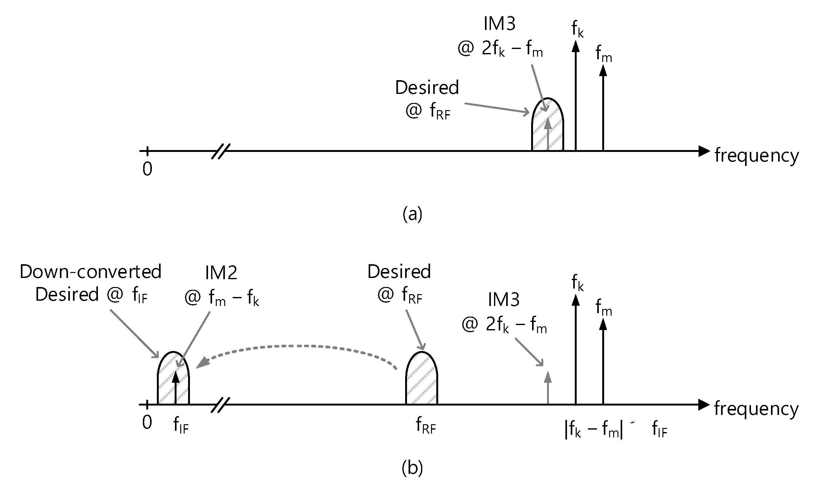
Figure 1a shows the first situation such that two subcarrier tones at
fk and
fm create the third-order intermodulation (IM3) distortion at 2
fk −
fm. The resulting IM3 falls inside the desired RF channel at
fRF, directly leading to SNR degradation at
fRF. Considering that the typical subcarrier spacing is in the range of a few 100 Hz to a few kHz for the communication and broadcasting signals, this effect is only possible when the two subcarrier tones are very close to
fRF. Such a close blocker signal will be likely to exist inside the desired band. Then, the in-band interference mitigation techniques such as the channel-scan-and-search-based LBT will be effective enough for its mitigation.
On the other hand, when the OFDM blocker signal is far away from
fRF as shown in
Figure 1b and is, thus, likely to be out of the MedRadio band, then its IM3 tone cannot directly affect the desired band at
fRF. Yet, the IM2 distortion at
fm −
fk will fall in the down-converted IF or baseband channel at
fIF and lead to the SNR degradation. The LBT technique that works for the close blocker signal will not work for this situation because the blocker signal is located far away out of the band and is, thus, likely out of the channel scan range.
It should be noted that a variety of communication and broadcasting services that are being offered worldwide in the UHF and VHF bands employs the OFDM signaling. Hence, the IM2 distortions induced by the OOB OFDM blocker signal need to be analyzed rigorously to accurately assess the SNR degradation in the MedRadio receiver.
Figure 2 illustrates that the OOB OFDM blocker signal at
fBL appears beside the desired MedRadio RF signal at
fRF. Let the number of subcarriers and subcarrier spacing of the OFDM blocker are
Nsub and
fsub, respectively. For example, in the ATSC 3.0 standard [
21], given the channel bandwidth of 6 MHz,
fsub is 843.7, 421.8, and 210.9 Hz depending on the OFDM FFT modes of 8K (
Nsub = 6913), 16K (
Nsub = 13,826), and 32K (
Nsub = 27,649), respectively. Similarly, we can find that
fsub is 279–8929 Hz for DVB-T2 [
22], and 992–3968 Hz for ISDB-T [
23].
As shown in
Figure 2, any combination of two subcarrier tones out of the total
Nsub subcarrier tones will create (
Nsub − 1) of IM2 tones at the baseband, starting from the first at
fsub to the last at (
Nsub − 1)·
fsub. If the desired IF signal band overlaps with the IM2 tones, the total IM2 distortion power can be computed by integrating its power spectral density (PSD) over the IF channel bandwidth. Then, the SNR degradation caused by the OFDM-induced IM2 distortions can be accurately evaluated. For example, the IF signal bandwidth of
Figure 2 encompasses the 3rd IM2 tone at 3⋅
fsub through the 10th IM2 tone at 10⋅
fsub. Thus, the total IM2 distortion power should be computed by integrating from the 3rd through the 10th IM2 distortion power.
The well-known input-referred second-order intercept point power (
IIP2) of an RF receiver is expressed as
where
Pin is the input power,
Pout is the output power, and
POIM2 is the output-referred IM2 distortion power, all expressed in dB or dBm. When a OFDM blocker signal that has the total power of
Pin.total is fed to a receiver having
IIP2 and a power gain of
GP, the input-referred IM2 distortion power
PIIM2 (=
POIM2 − GP) can be expressed by
If the total number of subcarriers is
Nsub, the power of each subcarrier
Pin.sub is given by
Now, let us compute the total input-referred IM2 distortion power by integrating the IM2 PSD over the band of interest. Ranjan et al. in their OFDM distortion analysis [
24] derived an analytic expression of the IM2 PSD by assuming that IM2 tones at the baseband are uncorrelated with the original causative OFDM data. Although the exact PSD expression (Equation (12) of [
24]) is not repeated here, we can find that the numerical integration of PSD can be simply carried out by collecting and adding the subcarrier PSD components at their center frequencies without a significant loss in generality and accuracy. Let us take an example of the 3rd
PIIM2 illustrated in
Figure 2, which is the first IM2 tone that exists in the IF band. We can find that the 3rd
PIIM2 is created by (
Nsub − 3) of two subcarrier tones that are apart by 3·
fsub in the original OFDM blocker signal. This observation can be generalized such that the
k-th IM2 power
PIIM2.kth can be obtained by
k-th
PIIM2 multiplied by the total number of the subcarrier pairs responsible for creating the
k-th IM2 tone. It is expressed by
If the band of interest covers from the
ki-th IM2 tone through the
kf-th IM2 tone, then, the total input-referred IM2 power
PIIM2.total that exists within the band of interest can be calculated by summing (
Nsub − k) of
PIIM2.kth of (4) from the first
ki-th through the last
kf-th. It is expressed as follows
Equation (5) can be written again in dB as follows
By substituting
Pin.sub of (6) with (3), Equation (6) can be arranged as
where
Poffset is given by
Equations (7) and (8) imply that the IM2 distortion power induced by the OFDM signal can be equivalently evaluated by the IM2 distortion power induced by the two-tone blocker signal as long as the two-tone blocker signal power is set to be lower than the original OFDM blocker signal power Pin.total by Poffset.
This finding greatly simplifies the simulation and characterization of the OFDM-induced IM2 distortion in an RF receiver. Involvement of a multi-carrier OFDM signal in RF circuit simulations will typically require a sophisticated OFDM signal modeling, a very complex numerical analysis method, and a long simulation time. Thus, it is very time-consuming and impractical to examine the OFDM-induced IM2 effects in RF circuit design. However, if the OFDM blocker signal can be replaced simply by an equivalent two-tone blocker signal by considering an offset parameter Poffset, the whole simulation process will become much simpler and more convenient because we can use the conventional time- and frequency-domain circuit simulation methods. Thus, these analytic results enable us to evaluate the OFDM-induced IM2 effects very efficiently when only examining an equivalent two-tone blocker induced IM2 effects.
Let us take an example of 16K FFT mode of ATSC 3.0 [
21], which has
Nsub = 13,825 and
fsub = 421.875 Hz. When the IF band of a low-IF MedRadio receiver resides in 150–450 kHz, the IM2 tones appearing within the band are from
ki = 356th to
kf = 1066th components. Then,
Poffset is computed to +6.56 dB by (8). It implies that if an ATSC blocker of −10 dBm is injected to a receiver and induces IM2 distortion at the baseband, the same amount of IM2 distortion power is also induced by a simple two-tone blocker of −16.56 dBm. Moreover, assuming the input signal power of the receiver is −50 dBm, and the receiver
IIP2 is +30 dBm,
PIIM2.total will be −63.1 dBm (=2 × (−10 − 6.56) − 30) according to Equation (7), and the resulting SNR will be +13.1 dB as the input signal power is −50 dBm and the input-referred distortion power
PIIM2.total is −63.1 dBm
3. Designs
Figure 3 shows the architecture of the MedRadio RF receiver. It is designed in an RF CMOS process. The receiver comprises a low-noise amplifier (LNA), transconductance (Gm) stage, quadrature down-conversion mixer with IM2 calibration, trans-impedance amplifier (TIA) with dc offset calibration (DCOC), three-stage variable gain amplifiers (VGAs), complex bandpass filter (BPF), fractional-N phase-locked loop (PLL) synthesizer, and a divide-by-4 local oscillator (LO) generator.
The receiver takes a low intermediate-frequency (IF) architecture employing a quadrature single down-conversion scheme. The IF frequency is set equal to the channel bandwidth of 300 kHz so that the down-converted IF band resides in 150–450 kHz.
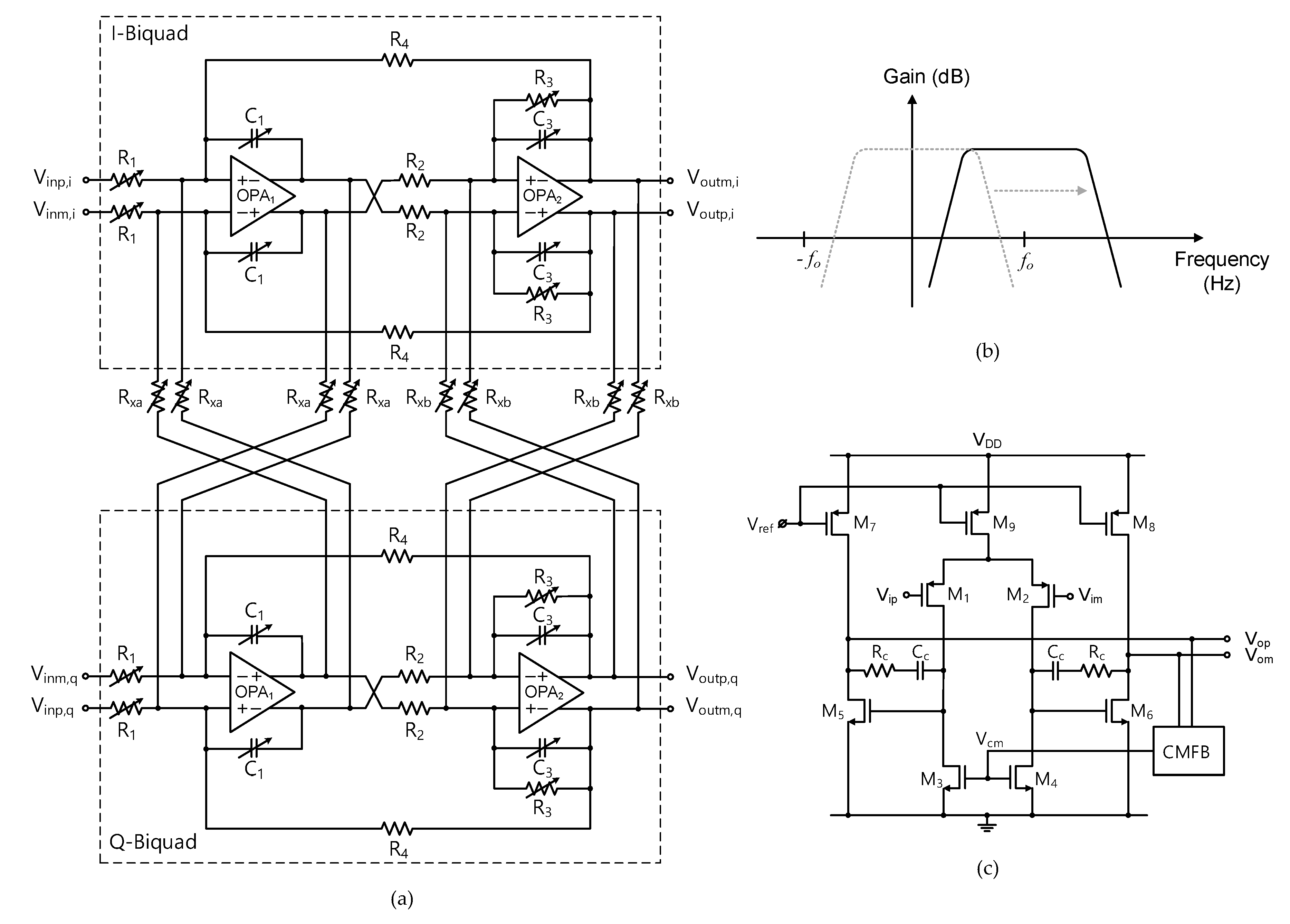
The image band of the desired RF signal is rejected by the complex BPF. As shown in
Figure 3, the complex BPF comprises two-stage complex biquads and three-stage VGAs. The detailed block diagram of the single-stage complex biquad is shown in
Figure 4a. The unit biquad is based on a modified Tow-Thomas low-pass filter (LPF) structure in which the lossless integrator block (OPA
1, C
1) is put before the lossy integrator block (OPA
2, R
3, C
3). Since the second-order filtering is given by the unit biquad, the overall two-stage complex BPF presents a fourth-order bandpass filtering characteristics.
Figure 4b illustrates how the low-pass characteristics of the unit biquad are translated to the complex bandpass characteristics. The cross-interconnecting resistors R
xa and R
xb that are placed between the I- and Q-path biquads as shown in
Figure 4a shift the complex conjugate poles to real poles, resulting in the original low-pass filter response being shifted to the desired complex bandpass filter response, which gives the image rejection capability [
25]. For optimal image rejection performance, the center frequency
fo is equally set to the channel bandwidth. As a result, the image component at the negative frequency band at −
fo is suppressed with respect to the wanted positive frequency band at +
fo. To cope with process variability and also to support variable channel bandwidth modes, key performance parameters of the complex biquad are tunable by realizing the on-chip resistors and capacitors in a switched value structure. The resulting switched tuning ranges are given by 34–136 kΩ with 2-bit control for R
1, 82–103 kΩ with 3-bit control for R
3, and 0.6–7.35 pF with 4-bit control for C
1 and C
3, while R
2 and R
4 are fixed to 135 kΩ. Then, the overall complex BPF shows a tunable gain of −22–+45 dB, tunable center frequency of 0.25–3 MHz, tunable bandwidth of 0.23–2.7 MHz, and tunable quality factor of 0.9–1.1. In addition, the passband flatness is also tunable by independently controlling the on-chip R
xa and R
xb in the range of 78–106 kΩ so that the band-edge gain difference is adjusted in the range of −1–+1 dB [
25].
Figure 4c is the schematic of the operational amplifiers OPA
1 and OPA
2. It is a fully differential two-stage amplifier with a dc common-mode feedback (CMFB). The first stage is a differential pair having
p-FET input pair of M
1,2 and
n-FET active load of M
3,4, and the second stage is
n-FET common-source stage of M
5,6. Designed parameters of the FET’s gate width/length are 200/0.2 μm for M
1,2, 80/0.5 μm for M
3,4, 64/0.2 μm for M
5,6, 192/0.5 μm for M
7,8, and 480/0.5 μm for M
9. The dc bias currents are 42 μA for M
9 and 18 μA for M
7,8. The frequency compensating R
C and C
C are 4 kΩ and 0.9 pF, respectively.
The LO signal is generated by the fractional-N PLL frequency synthesizer. A 20-bit digital delta-sigma (Δ∑) modulator is employed for the fractional-N frequency generation. Details of this PLL can be found in the author’s prior work [
26]. The voltage controlled oscillator (VCO) covers 1.4–1.8 GHz, which is 4× higher than the MedRadio RF band of 401–406 MHz. The automatic frequency calibration (AFC) searches for an optimal sub-band out of the 32 sub-bands through 5-bit switched capacitor bank of the VCO. The divide-by-4 LO generator circuit after the VCO buffer generates I/Q LO signals with 25% duty cycle for driving the mixer FETs. The 25% duty-cycle LO signal improves the conversion gain and noise figure performances of the quadrature mixer [
17].
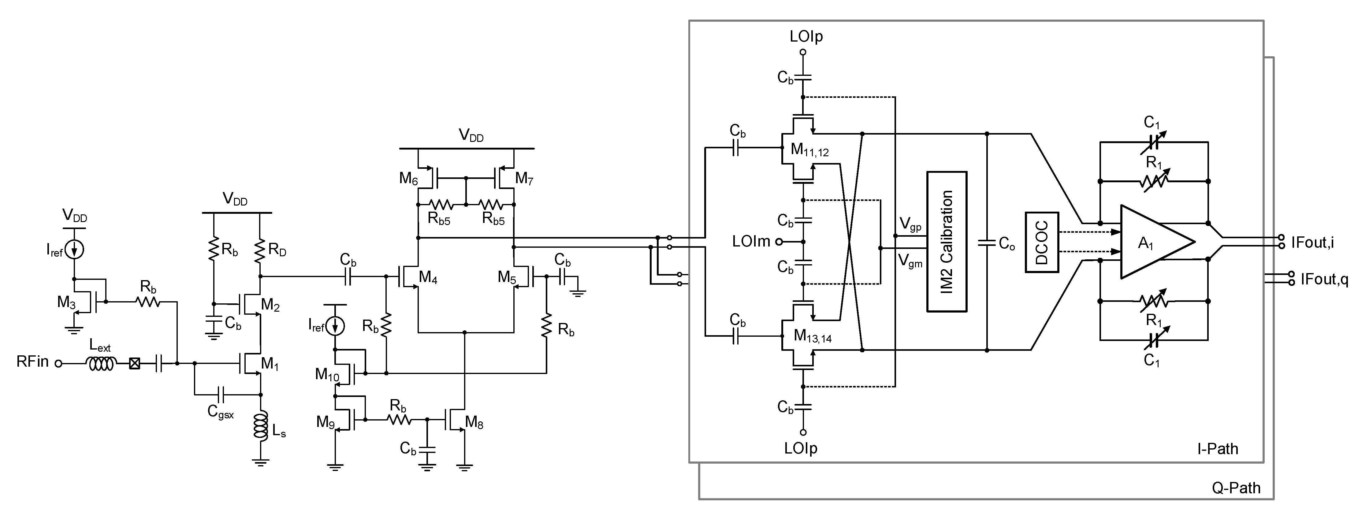
Figure 5 shows the detailed circuit schematic of the RF front end. The LNA is based on the single-ended cascode structure with M
1,2 (gate width = 128 μm, gate length = 60 nm) and a resistive load R
D (408 Ω), dissipating 520 μA. The source degeneration inductor L
s of 9 nH and the additional gate-to-source capacitor C
gsx of 0.74 pF are used for simultaneous noise and power matching. The input impedance matching is achieved only by a single off-chip inductor L
ext (132 nH). The G
m stage with M
4,5 (gate width = 5.6 μm, gate length = 60 nm) and M
6,7 (gate width = 16 μm, gate length = 60 nm) performs a single-to-differential conversion for interfacing between the single-ended LNA and differential mixer. It also prevents a severe degradation of the LNA performance that can be otherwise caused by the low input impedance of the passive mixer. The passive mixer with M
11,14 (gate width = 14 μm, gate length = 60 nm) is adopted for the benefits of the low power dissipation and low 1/f noise. The differential I/Q LO signals LOI
p,m and LOQ
p,m are fed to the mixer via ac-coupling capacitors C
b (10 pF).
The TIA comprises an operational amplifier A1 and feedback components R1 and C1. The R1 and C1 are designed in a switched value structure for achieving the bandwidth tunability between 3.4 and 9.5 MHz. R1 is switchable among 2, 8, 9, and 10 kΩ, and C1 is switchable between 0 and 3.5 pF with 0.5 step. The A1 is a fully differential two-stage structure with its gain bandwidth product of 21.6 MHz. The total gain of the RF front end is +42.2 dB.
The IM2 calibration at the mixer is designed to minimize the IM2 distortion. It is generally known that the IM2 distortion created by FET non-linearities is manifested by the differential mismatches in FETs, dc bias voltages, passive impedances, and layout routings. Thus, the differential mismatches need be minimized to suppress the IM2 distortion at the receiver output. In this design, as proposed in [
27,
28], the dc gate bias voltages V
gp and V
gm for the switch FET’s M
11–14 are controlled by employing a 6-bit R-2R digital-to-analog converter (DAC). The DAC needs to have a fine-tuning resolution for precise IM2 calibration, but a higher number of total bits will make the calibration process slow. Thus, in order to overcome the two conflicting requirements of the fine resolution and lower number of control bits, we set the full scale of the DAC to a significantly reduced value of only 50 mV, while its common-model level is tunable for a wider range between 0.5 and 0.9 V by using another 3-bit DAC. As a result, the gate bias tuning resolution is as fine as 0.78 mV. In this work, the IM2 calibration is done manually by monitoring the IM2 level with respect to the mixer gate bias voltages. In a practical mass-production stage, this IM2 calibration can be done more efficiently by using automatic test equipment (ATE).
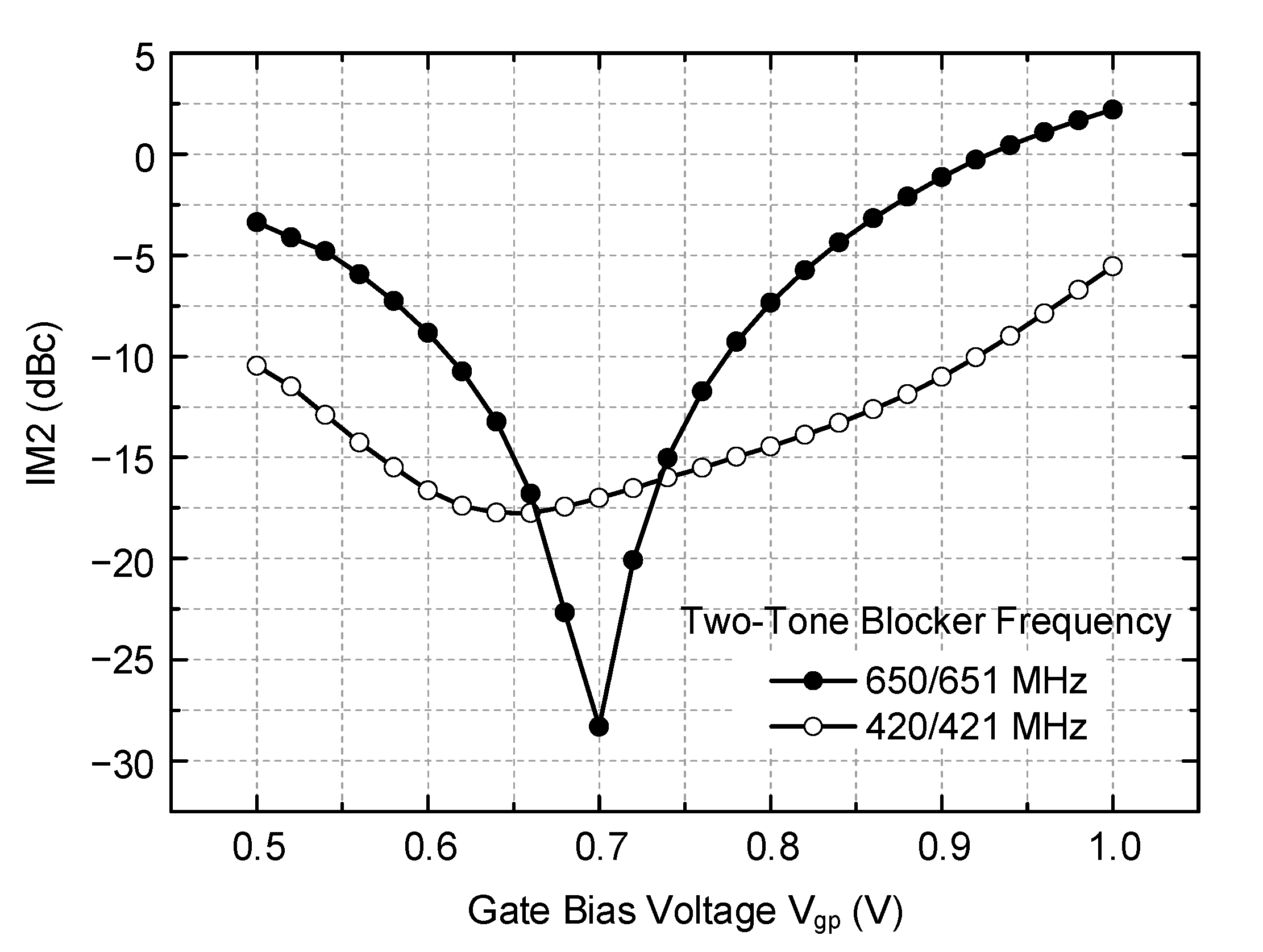
IM2 calibration is verified through circuit simulations.
Figure 6 shows simulation results. The desired RF input of −30 dBm at 402 MHz is injected, and the OOB two-tone blockers of −10 dBm at (420, 421 MHz) in one simulation and (650, 651 MHz) in the other simulation are injected. With the LO frequency set to 404 MHz, the wanted IF signal appears at 2 MHz, while the IM2 distortion appears at 1 MHz. The IM2 distortion power with respect to the wanted tone power is examined with the gate bias voltage V
gp tuned from 0.5 to 1.0 V, while the other gate bias V
gm is fixed at 0.7 V. As can be seen, the IM2 distortion level is drastically reduced when the gate bias voltage V
gp is set to an optimal point, which is 0.65 V for 420/421 MHz blocker and 0.7 V for 650/651 MHz blocker. It clearly implies that any unwanted mismatches that are inevitable during the circuit fabrication processes can be successfully compensated by the proposed IM2 calibration circuit, thus guaranteeing a satisfactory IM2 distortion level in the receiver.
Meanwhile, it is found that the proposed IM2 calibration circuit creates an unwanted dc level change at the mixer output during the IM2 calibration. Since the signals from mixer output to the TIA, the first VGA, and the first biquad are all dc-coupled, the dc level changes at the mixer output will directly lead to a significant dc offset at the first biquad output of the complex BPF. The dc offset must be cancelled out even though the down-converted signal resides in the low-IF band and not in dc. It is because the residual dc offset created by the preceding IM2 calibration will harmfully reduce the dynamic range of the following stages. In the conventional low-IF receiver designs, for example, that reported in [
12,
29], the signals after the mixer output are ac-coupled. Then, the dc offset can be cancelled out by directly controlling the gate biases of the input FETs of a subsequent stage. However, in this design, that approach cannot be taken because the gate bias tuning will adversely alter the optimum IM2 calibration condition obtained at the previous mixer stage. Thus, in this work, we tune the body bias voltages of the input FETs of A
1 to cancel out the dc offset. This approach successfully cancels the dc offset at the biquad output, while avoiding the adverse interaction with the IM2 calibration condition at the mixer.
4. Results and Discussions
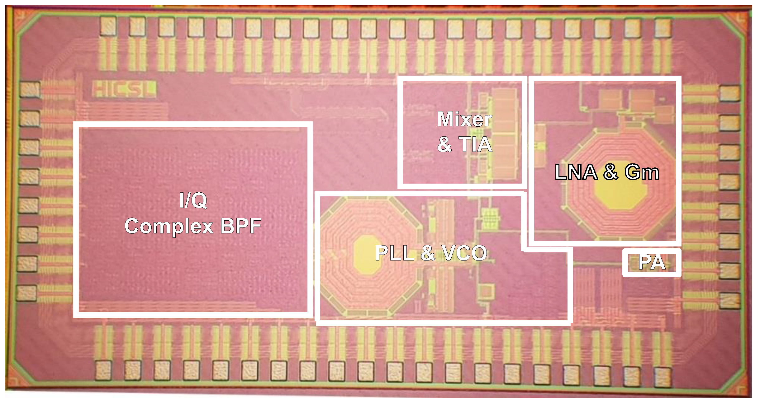
The MedRadio receiver is fabricated in a 65 nm RF CMOS process. A micrograph of the fabricated chip is shown in
Figure 7, in which the major building blocks are denotated. Note that the chip includes not only the RF receiver of
Figure 3 but also an RF transmitter comprising a divide-by-4 circuit and a class-D power amplifier. However, the design details and measurement results of the RF transmitter are not discussed in this paper because they are out of the scope. Nevertheless, the total die size including the entire receiver and transmitter is 2.46 × 1.26 mm
2. The fabricated die is mounted and directly wire-bonded on a printed circuit board for experimental measurements. A single supply voltage of 1 V is used.
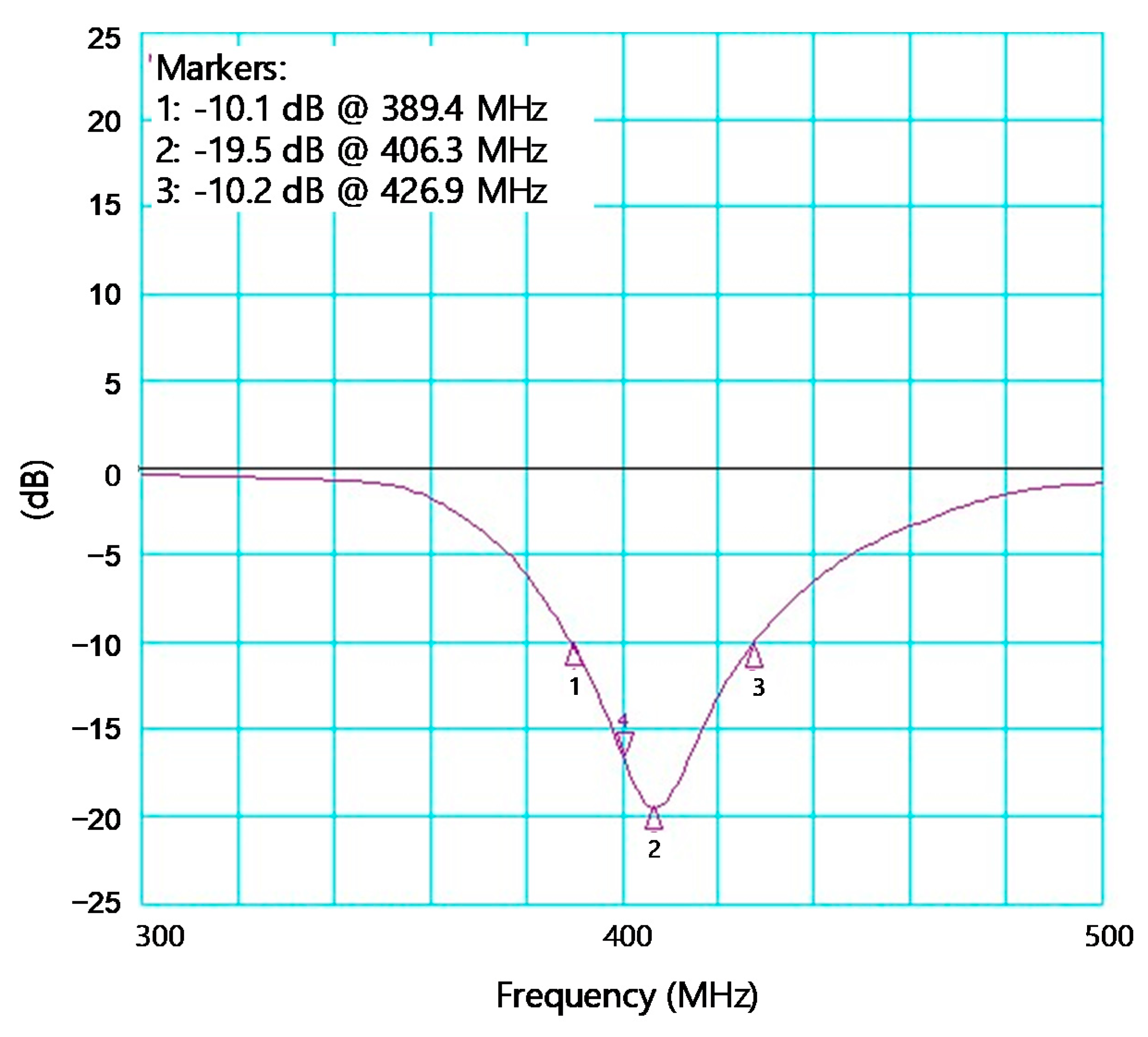
Figure 8 shows the measured S
11 of the receiver. The input impedance bandwidth having S
11 < −10 dB is 37.5 MHz between 389.4 and 426.9 MHz. It shows that the single series off-chip inductor L
ext shown in
Figure 5 is enough to achieve the satisfactory input bandwidth for the MedRadio applications. Note that this external L
ext is not changed during the subsequent whole OOB blocker measurements.
The measured gain and noise figure performances of the RF front end are plotted in
Figure 9. The measurements were done by probing intermediate test ports at the TIA output. The gain is measured by applying the RF and LO signals by using signal generators and reading the output power level by using a spectrum analyzer (N9030B of Keysight Technologies Inc., Santa Rosa, CA, USA). The measured passband gain of the RF front end is +42.2 dB. As shown earlier in
Figure 5, the on-chip feedback components R
1 and C
1 of the TIA are tunable. By controlling these, the TIA bandwidth is tuned between 3.4 and 9.5 MHz in eight steps. Among them,
Figure 9 only displays three selected curves corresponding to the minimum 3.4 MHz, medium 4.9 MHz, and the maximum 9.5 MHz conditions for the TIA bandwidth.
For the noise figure measurement, the total output noise power
Pn,out with the input port terminated by 50 Ω is measured by using the spectrum analyzer. With
Pn,out and the receiver’s power gain G
P are known, the receiver noise figure is calculated by (
Pn,out + 174 dBm/Hz −
GP). This method is convenient because it does not need a noise source or noise figure meter and also ensures sufficient accuracy because the noise floor level of the spectrum analyzer is more than 30 dB lower than
Pn,out. The measured noise figure at the low-IF band of 150–450 kHz is given by 3.7–4.5 dB. Assuming that a non-coherent detection for binary frequency shift keying (BFSK) signal is adopted, the minimum required SNR should be 14 dB for achieving a bit error rate (BER) of 10
−6. In practice, the minimum BER required by a raw RF radio excluding a digital processor can be as high as ~ 10
−3 [
5], and the required SNR for this can be further lower by 3 dB, that is, only 11 dB. However, in order to take various practical errors and margins into account, we decide to use 14 dB for the minimum required SNR in the following discussions. Note that the receiver sensitivity
Psens is given by
where
NF is the receiver noise figure,
B is the signal bandwidth,
SNRmin is the minimum required SNR. With
SNRmin = 14 dB,
B = 300 kHz, and
NF = 4.5 dB, the receiver sensitivity
Psens is calculated to be −100.7 dBm or 2.06 μVrms. This sensitivity performance is comparable to [
12,
15] and much better than [
5,
13].
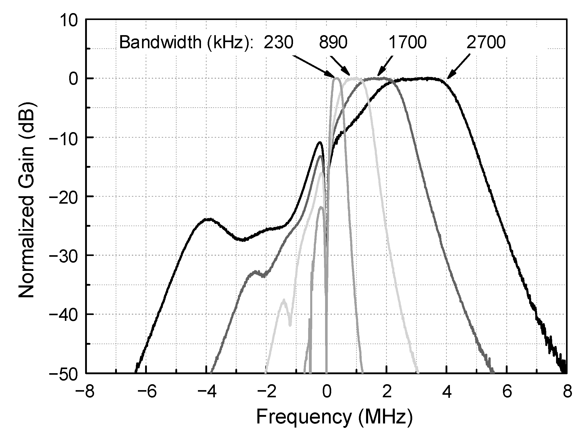
Figure 10 shows the measured frequency responses of the complex BPF. The measured curves exhibit the bandwidth tuning and image rejection performances at a medium gain condition. Although not shown here, the gain is also tunable between −22.5 and +45.4 dB in 24 steps. However, normalized gains are drawn in
Figure 10 for the sake of clarity. The bandwidth is tunable between 230 and 2700 kHz in 16 steps by tuning the switched resistor and capacitor components R
1, C
1, R
3, and C
3 in
Figure 4.
Figure 10 only displays the four selected curves out of the total 16 curves. The image rejection ratio can be evaluated by taking the ratio of the two gain values, one at the passband’s center-frequency point and the other at its image-frequency point. The resulting image rejection ratio is 26.4–33.3 dB, which is sufficient enough considering that the minimum required SNR is 14 dB.
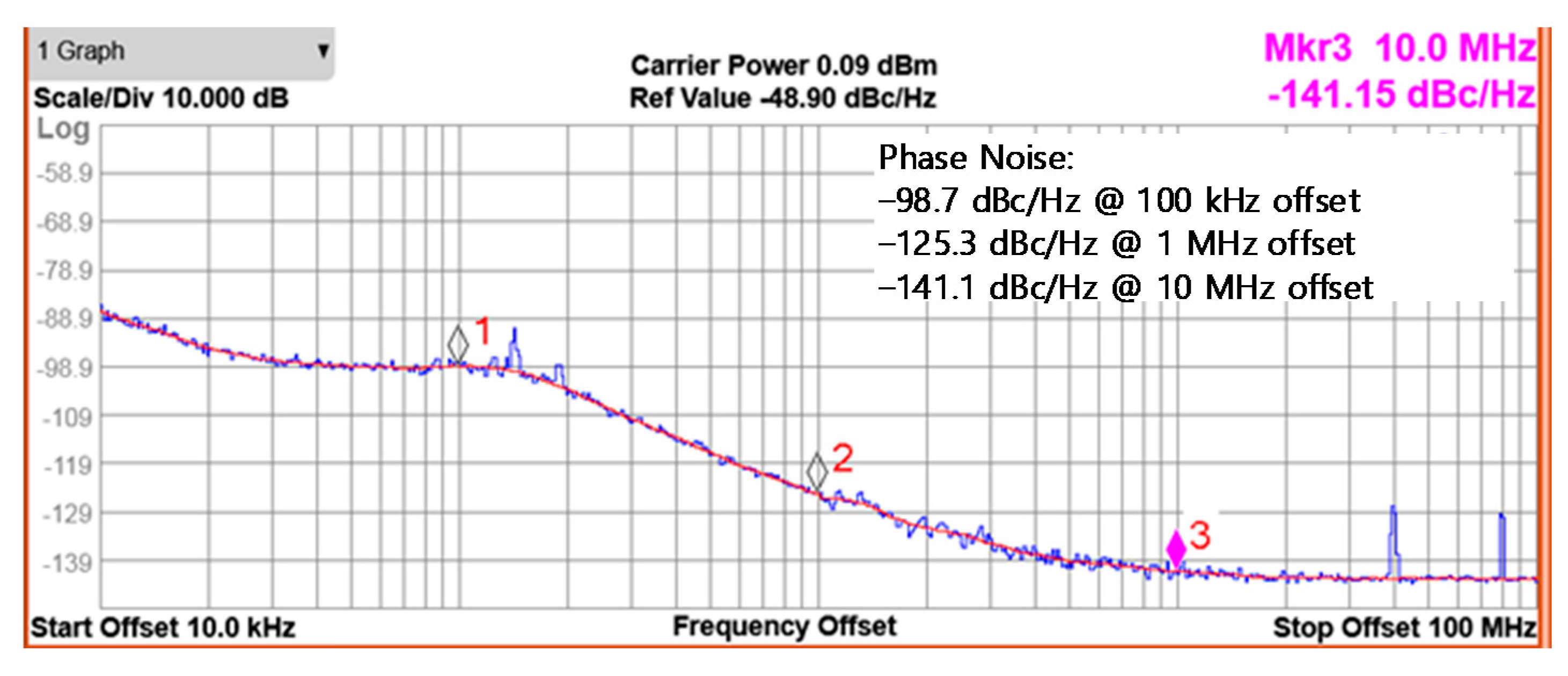
Figure 11 is the measured phase noise of the PLL synthesizer at the output frequency of 400 MHz. The measured phase noise is −98.7 and −125.3 dBc/Hz at 100 kHz and 1 MHz offsets, respectively. The phase noise performance is comparable to the previously reported similar LC VCOs in [
12,
17], whereas it is much better than [
30] for the same MedRadio applications because of the LC cross-coupled structure rather than the ring oscillator structure.
The IM2 calibration is verified through extensive measurements over more than five samples. All results show reasonably good agreements with acceptable variability.
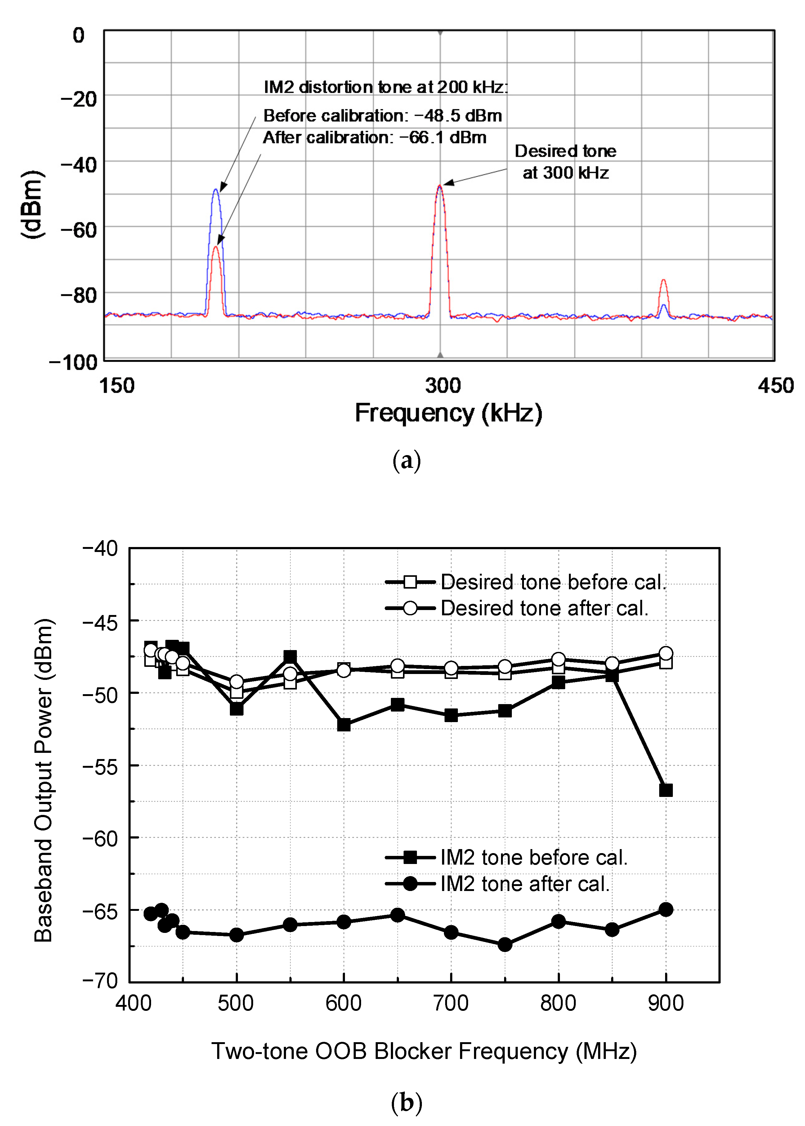
Figure 12a shows the measured spectrum, demonstrating how the IM2 distortion is suppressed by the proposed IM2 calibration. The desired RF single tone of −90 dBm at 403.5 MHz are fed to the receiver together with two-tone blocker of −50 dBm at 433.0 and 433.2 MHz. The receiver is set to a nominal gain condition. Then, the wanted IF and unwanted IM2 tones appear at 300 kHz and 200 kHz, respectively. Before the IM2 calibration, the desired and distortion tones are −47.8 and −48.5 dBm, respectively. After the IM2 calibration is carried out, the desired tone power does not show a noticeable change, whereas the IM2 tone power is significantly reduced from −48.5 dBm to −66.1 dBm. As a result, the signal-to-IM2-distortion ratio is improved from +0.7 dB to +18.3 dB. It implies that before the calibration, the receiver cannot satisfy the 14 dB SNR requirement, but after the calibration, it successfully satisfies the SNR requirement with a sufficient margin of 4.3 dB.
The IM2 calibration measurements are further carried out over the entire UHF band between 420 MHz and 900 MHz, and the results are plotted in
Figure 12b. It is observed that the IM2 distortion is suppressed typically by 15 dB in the range of 8.3–20 dB through the IM2 calibration, while the desired tone remains almost unchanged.
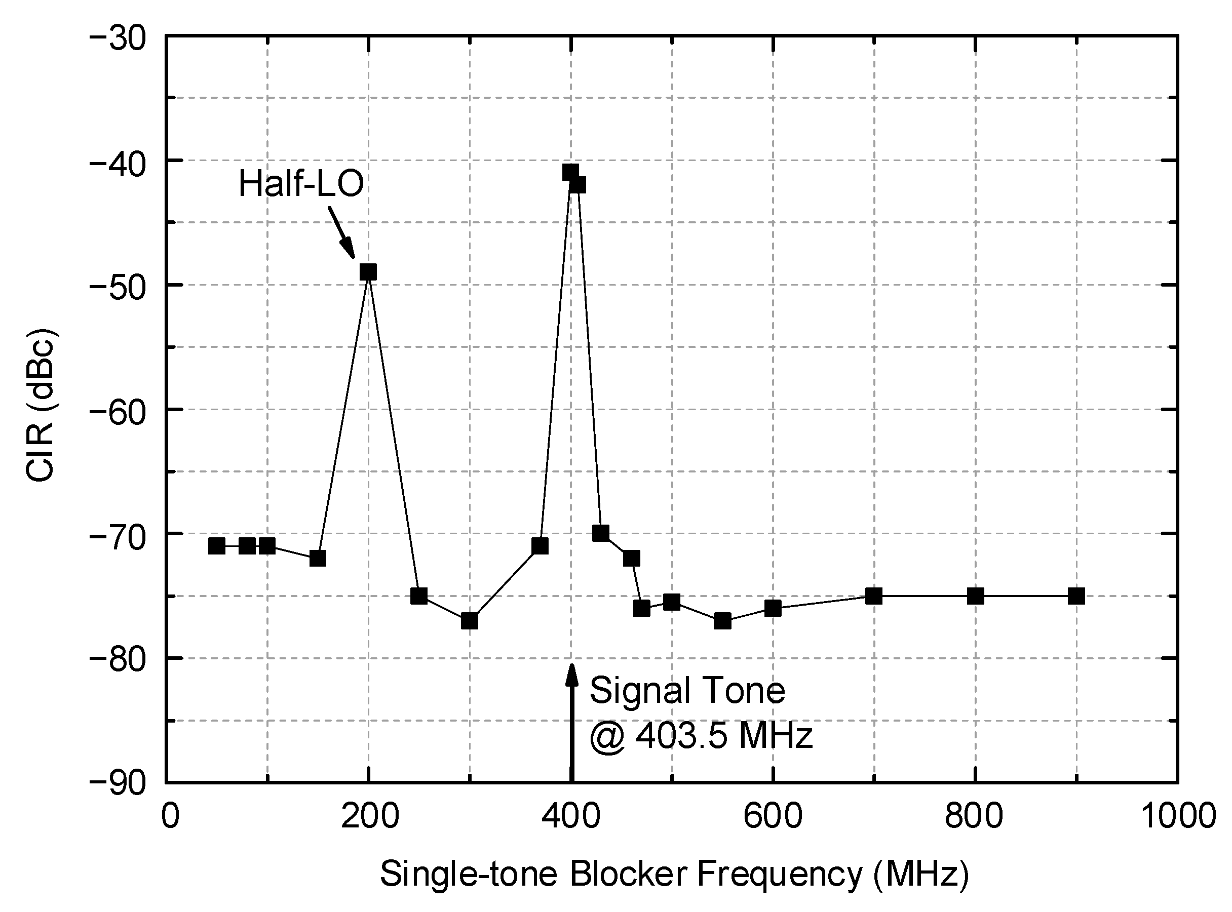
The interference tolerance performances of the receiver against the OOB two-tone blocker are evaluated through the carrier-to-interference ratio (CIR) measurements and plotted in
Figure 13. The maximum tolerable CIR is measured as following. First, a −90 dBm desired signal at 403.5 MHz is fed to the receiver, and an OOB two-tone blocker with 200 kHz spacing between 420 and 900 MHz is injected together. Then, the blocker signal power is raised until the output SNR reaches 17 dB. Note that we use a 3 dB higher SNR requirement for this CIR test by considering that any more noise and distortion contributions other than this IM2 distortion can be additionally involved in practice. Then, the ratio of the signal and blocker power at this 17 dB SNR condition is defined as the maximum tolerable CIR. The measured results are plotted in
Figure 13. The maximum tolerable CIR indicates the receiver’s selectivity performance against the two-tone blocker. As can be seen in
Figure 13, the proposed IM2 calibration effectively improves the CIR by 4–11 dB across the UHF band. The CIR after the calibration is −40.2 dBc at 420 MHz, which is very close to the in-band, and gradually improves up to −71.2 dBc as the blocker frequency moves farther away out of the band. The measured CIR can also be translated to the maximum tolerable two-tone blocker power of −49.8–−18.8 dBm. Then, considering
Poffset = 6.56 dB as discussed in
Section 2, we can conclude that the equivalent OFDM blocker power of −43.2–−12.2 dBm can be tolerated by this RF receiver.
Another important interference tolerance is against a single tone blocker. The measured results are plotted in
Figure 14. The desired signal power is set to −98 dBm at 403.5 MHz, which is 3 dB higher than the sensitivity level. The single-tone blocker signal across the VHF and UHF band is injected together, and its power is raised up to a point such that the output SNR becomes 17 dB in the same reason described earlier. The CIR at a frequency that is only 4 MHz away from the desired tone is found to be −41 dBc, which corresponds to the maximum tolerable single-tone blocker power, is −57 dBm. However, in general, the maximum tolerable CIR shows much better performance as low as −70–−77 dBc for the rest of the band between 50–370 MHz and 430–900 MHz. One exception is observed at a half LO frequency near 200 MHz, where the CIR is observed to be −49 dBc. Although the MedRadio standard [
1] does not clearly state this, such a limited set of exceptions would be generally accepted for the overall system operations because it can be avoided through high-level channel classification and a search process as is typically done in the Bluetooth receiver for internet-of-things (IoT) applications [
28,
29].
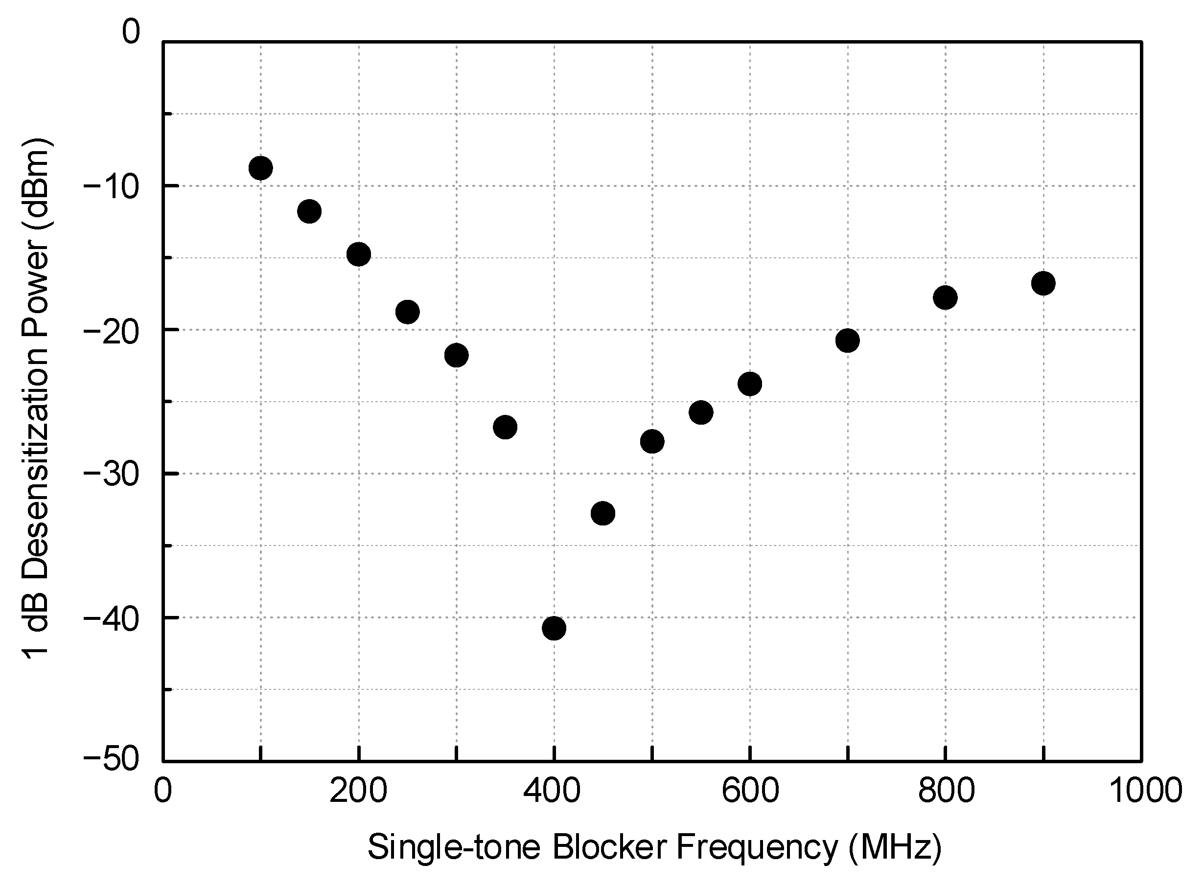
The 1 dB gain desensitization against the single-tone blocker is measured and shown in
Figure 15. The worst point appearing at 403.5 MHz corresponds exactly to the input-referred 1 dB compression power (
IP1dB) of the receiver, which is −40.8 dBm. As the blocker frequency moves away from the in-band, the 1 dB desensitization power continually grows from −26.7 dBm at 350 MHz to −9 dBm at 100 MHz for the lower band and also from −32.7 dBm at 450 MHz to −16.8 dBm at 900 MHz for the upper band.
Key performances of this work are summarized and compared with previous CMOS MedRadio receivers in
Table 1. It should be noted that most of the previous works [
4,
5,
12,
14,
15,
16] did not address the OOB blocker tolerance performances. Only a few works reported selectivity performances. Cho et al. [
18] reported an OOB CIR of −30 dBc against the VHF band interference between 30 and 70 MHz, and Ba et al. [
12] demonstrated the ACR performance of 15 dB in their MedRadio receiver. Huang et al. [
19] reported the CIR of −10 dB in their 915 MHz OOK receiver. Such performances should be compared to the CIR against the single tone blocker of this work. As discussed in
Figure 14, this work shows much better performance, which is better than −41 dBc without an exception, or even better than −70 dBc if two exceptions are allowed at the half LO and 4 MHz away in-band frequencies. As can be seen in
Table 1, this work is the first reporting the OOB CIR performances against the two-tone and single-tone blockers, which can be translated to the maximum tolerable OOB blocker power levels. Additionally, the maximum tolerable CIR against the two-tone blocker can be translated to the maximum tolerable CIR against the OFDM blocker when the
Poffset of Equation (8) is taken into account.


