
Gradually Modified Conductance in the Self-Compliance Region of an Atomic-Layer-Deposited Pt/TiO2/HfAlOx/TiN RRAM Device

Division of Electronics and Electrical Engineering, Dongguk University, Seoul 04620, Korea
*
Author to whom correspondence should be addressed.
Metals 2021, 11(8), 1199; https://doi.org/10.3390/met11081199
Submission received: 3 July 2021
/
Revised: 21 July 2021
/
Accepted: 23 July 2021
/
Published: 28 July 2021
(This article belongs to the Special Issue Machine Learning Methods and Sustainable Development: Metal Oxides and Multilayer Metal-Oxides)
Abstract
:This study presents conductance modulation in a Pt/TiO2/HfAlOx/TiN resistive memory device in the compliance region for neuromorphic system applications. First, the chemical and material characteristics of the atomic-layer-deposited films were verified by X-ray photoelectron spectroscopy depth profiling. The low-resistance state was effectively controlled by the compliance current, and the high-resistance state was adjusted by the reset stop voltage. Stable endurance and retention in bipolar resistive switching were achieved. When a compliance current of 1 mA was imposed, only gradual switching was observed in the reset process. Self-compliance was used after an abrupt set transition to achieve a gradual set process. Finally, 10 cycles of long-term potentiation and depression were obtained in the compliance current region for neuromorphic system applications.
1. Introduction
Resistive switching behavior is observed in many dielectrics under an electric field [1]. The non-volatile resistance states are reversible in the high-resistance and low-resistance states. The types of switching are largely divided into unipolar and bipolar switching [2]. The memory state of the unipolar resistive switching memory can be changed by the electric stress at the same polarity. The reset process from a low-resistance state (LRS) to a high-resistance state (HRS) occurs by rupture of the conducting filament by Joule heating [3]. In contrast, the set and reset processes of the bipolar resistive type occur via the opposite polarity of the electric field. Among the many resistive switching materials, metal oxides are the most popular, owing to their good stability, reproducibility, and repeatability [4,5,6,7,8,9,10,11,12,13,14,15,16,17]. Representative metal oxide-based resistive random access memory (RRAM) materials include TaOx, TiO2, Al2O3, and HfO2 [4,5,6,7,8,9,10,11,12,13,14,15,16,17], with different configurations like anodic oxidation and physical vapor deposition (PVD), and chemical vapor deposition (CVD). It is worth noting that a bilayer stack of metal oxide exhibits relatively better resistive switching performance, such as endurance, retention, and variability performance, compared with a single-layer stack [18,19,20,21,22]. In a previous study, low-power operation was achieved by controlling oxygen vacancies in the case of a HfO2/TiOx bilayer RRAM [20]. In another study, the switching uniformity was improved for a HfO2/TiO2 bilayer device owing to stabilized filament formation and rupture [21]. In the case of a double insulating layer sandwiched by electrodes with a large difference in work function, self-rectifying I–V curves have been reported, which can reduce the sneak current in the cross-point array [22].
Resistive switching dielectrics can be deposited by various methods, such as sputtering. Atomic layer deposition (ALD) systems have the advantages of uniform deposition, excellent step coverage, and accurate thickness control [23]. Therefore, they are suitable for a 3D vertical RRAM structure [24] as well as a conventional 2D cross-point RRAM structure.
Neuromorphic systems are being studied to implement a better and more efficient computing system than the existing von Neumann computing structure [25]. Neuromorphic computing enables data operation and storage to be processed as closely as possible. Parallel data processing with low energy is achieved by adopting a structure in which the RRAM element array acts as an artificial synapse [26,27,28,29,30]. To implement an RRAM-based synaptic array in a neuromorphic system, it is important that the state of RRAM has a multi-level cell (MLC) [26,27,28,29,30]. Therefore, gradual change in the conductance value in an RRAM device is essential to obtain MLCs easily. Through gradual conductance changes, synaptic plasticity is imitated frequently [26,27,28,29,30]. To achieve a gradual change, the current of a RRAM cell should not be changed abruptly by the applied electric field. Filamentary-type resistive switching generally exhibits an abrupt transition in the set process [31]. There have been reports of a gradual transition in the set process using a bilayer stack [32,33]. This gradual set process, by self-compliance, could improve the synaptic properties of a neuromorphic system. A Ti/TaOx/HfO2/Pt device exhibits gradual set and reset processes owing to the oxygen reservoir of the thin TaOx layer [32]. In addition, a Ni/SiN/Al2O3/TiN device shows gradual set and reset I–V characteristics due to the tunnel barrier of Al2O3 [33].
In this study, we demonstrated gradual synaptic modulation in an ALD-deposited TiO2/HfAlOx RRAM device. So far, not much has been reported about ALD-deposited TiO2-based resistive memory. In previous studies, it was found that a high-k alloy type RRAM device can adjust the dielectric band gap while controlling the composition ratio, which can tune the resistance change switching properties [11,34].
2. Materials and Methods
A Pt/TiO2/HfAlOx/TiN RRAM device was prepared as follows. A 100 nm thick TiN layer was deposited on a SiO2/Si wafer via reactive sputtering. Thereafter, a 7 nm thick HfAlOx layer was deposited by the ALD system. Tetrakis (ethylmethylamino) hafnium (TEMAH) and trimethylaluminum (TMA) were used as the metal precursors for the HfO2 and Al2O3 layers, respectively. H2O was used as the oxidant for both layers. One cycle of (TMA + H2O) deposition and 11 cycles of (TEMAH + H2O) deposition were conducted for the alloyed-type dielectric. Next, a 7 nm thick TiO2 layer was deposited using titanium tetraisopropoxide (TTIP) and H2O as reactants. Finally, a 100 nm thick Pt layer was deposited using an electron-beam evaporator via a shadow mask with circular patterns 100 µm in diameter. XPS depth analysis was conducted using a Nexsa photoelectron spectrometer (Thermo Fisher Scientific, Waltham, MA, USA) with a microfocus monochromatic X-ray source (Al-Kα (1486.6 eV)), a sputter source (Ar+), an ion energy of 2 kV, a sputter rate of 0.5 nm/s for SiO2, and a beam size of 100 µm. The current–voltage (I–V) curves and transient curves of the RRAM cells were measured using a semiconductor parameter analyzer (Keithley 4200-SCS and 4225-PMU ultrafast module, Keithley Instrumnets, Cleveland, OH, USA), while a bias was applied to the Pt top electrode, and the TiN bottom electrode was grounded.
3. Results and Discussion
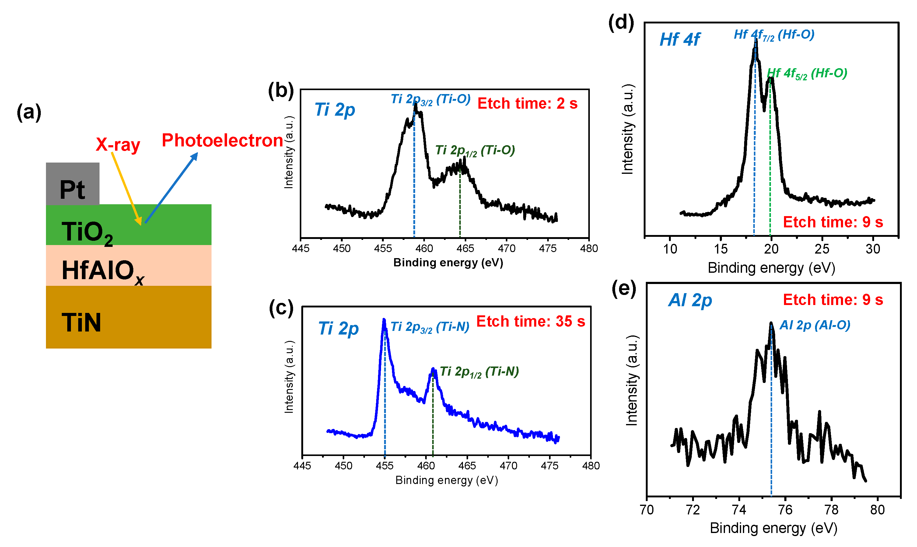
Figure 1a shows a schematic of the Pt/TiO2/HfAlOx/TiN device. XPS analysis was performed as the X-ray was incident from the TiO2 surface, and analysis was conducted on the inner thin film through Ar+ etching. Overall, ALD-deposited film had better stoichiometry compared with films deposited by other sputtering systems [35]. Figure 1b,c shows the Ti 2p spectra for an etch time of 2 s and an etch time of 35 s, which correspond to the TiO2 layer and the TiN bottom electrode, respectively. The Ti 2p XPS spectra included Ti 2p3/2 and Ti2p1/2, as shown in Figure 1b,c. The peak binding energies of Ti 2p3/2 and Ti 2p1/2 were located at approximately 458.94 eV and 464.5 eV for Ti-O bonds [36]. However, the peak binding energies of Ti 2p3/2 and Ti 2p1/2 were found at approximately 454.92 eV and 460.93 eV for Ti-N bonds [37]. Figure 1d shows the Hf 4f spectra at an etch level of 9. Hf 4f7/2 and Hf 4f5/2 doublet peaks were found at 18.63 eV and 20.03 eV, respectively, for Hf-O bonds in the Hf-dominated HfAlOx film. Figure 1e shows the Al 2p spectra at an etch time of 9 s. Because the Al content was low in the HfAlOx film, the Al intensity was low and some noise was observed, but a distinct peak was observed for the Al-O bond at approximately 75.4 eV [12].
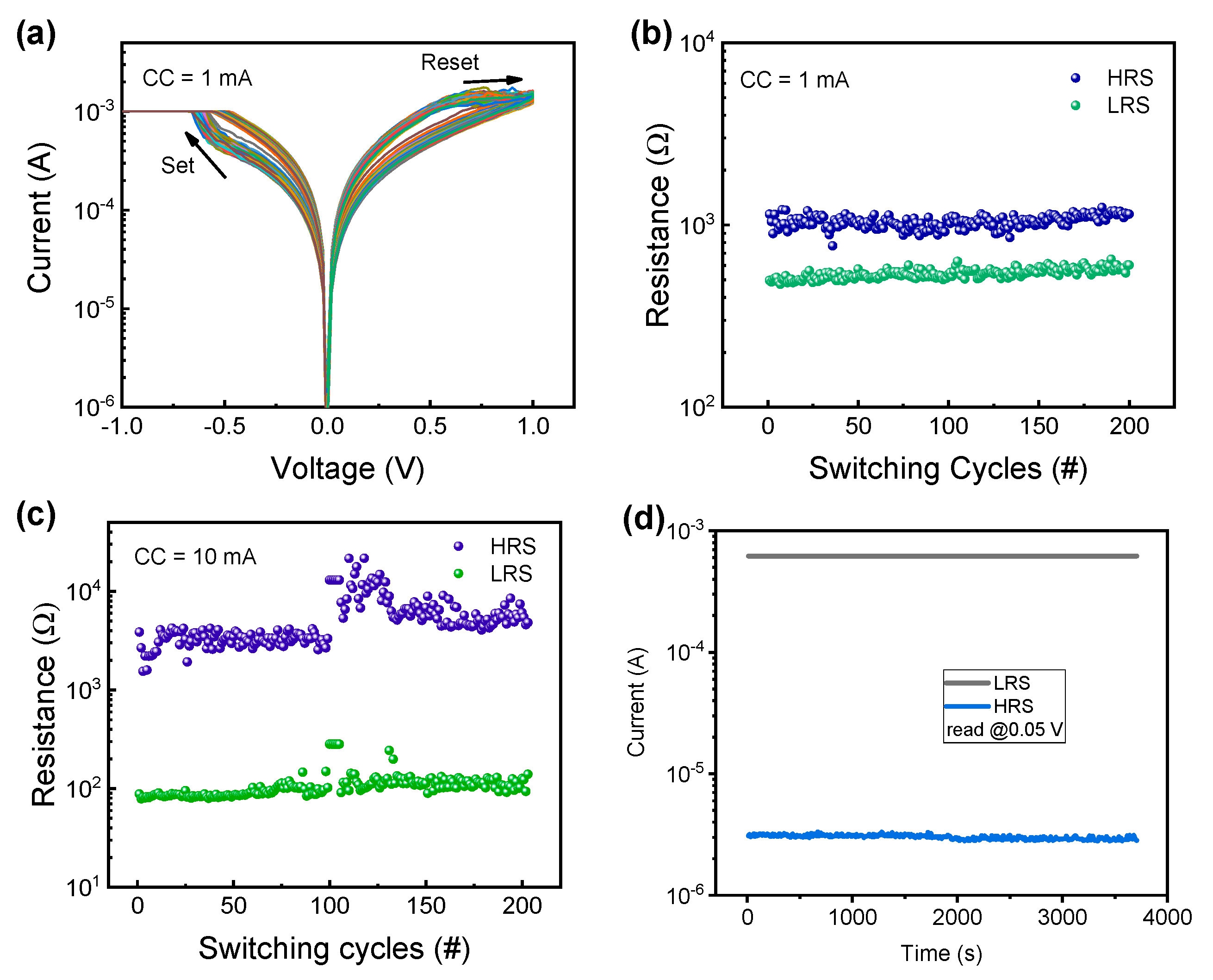
Figure 2a shows the I–V current characteristics, including 200 cycles of the Pt/TiO2/HfAlOx/TiN device. It was noted that initial forming curve is similar to the subsequent I–V curve of the set process, indicating that the device can be operated with a constant set voltage without the need for an additional forming process. We used filamentary model for resistive switching here, referring to existing literature [38,39]. The set process occurred by sweeping from 0 V to –0.7 V. An abrupt set transition was observed from the HRS to LRS, in which the decrease in resistance was due to soft breakdown in the two insulator layers. Here, a compliance current (CC) of 1 mA was used to control the conducting filament. Moreover, the oxygen vacancies in the double insulating layers were created under the applied bias [40]. It should be noted that the negative bias on the Pt/TiO2/HfAlOx/TiN device is relatively more favorable for resistive switching because the TiON interfacial layer acts as an oxygen reservoir [41]. The oxygen can easily move to the TiN layer to form TiON when a negative bias is applied on Pt. The detailed mechanisms have been discussed in previous studies [34,40,42]. The reset process was conducted to return the device to the HRS by sweeping from 0 V to 1 V. The reset process occurs because of the rupture of the conducting filament based on oxygen vacancies. The oxygen ions move from the TiON layer under a positive bias, and the recombination occurs with oxygen vacancies. Subsequently, the conducting filament can be ruptured, which indicates a decrease in conductance. Figure 2b shows up to 200 cycles, in which LRS and HRS possessed a read voltage of 0.3 V. Uniform LRS and HRS were achieved even though a small on/off ratio was observed. To increase the on/off ratio, the CC and reset stop voltages can be increased. The LRS current increased with an increase in CC, and the HRS current decreased with an increase in the reset stop voltage. An on/off ratio of 10 times or more was achieved by a CC of 10 mA and a reset sweep voltage of 2 V for 200 endurance cycles, as shown in Figure 2c. Good retention properties in the LRS and HRS were observed for 1 h (Figure 2d).
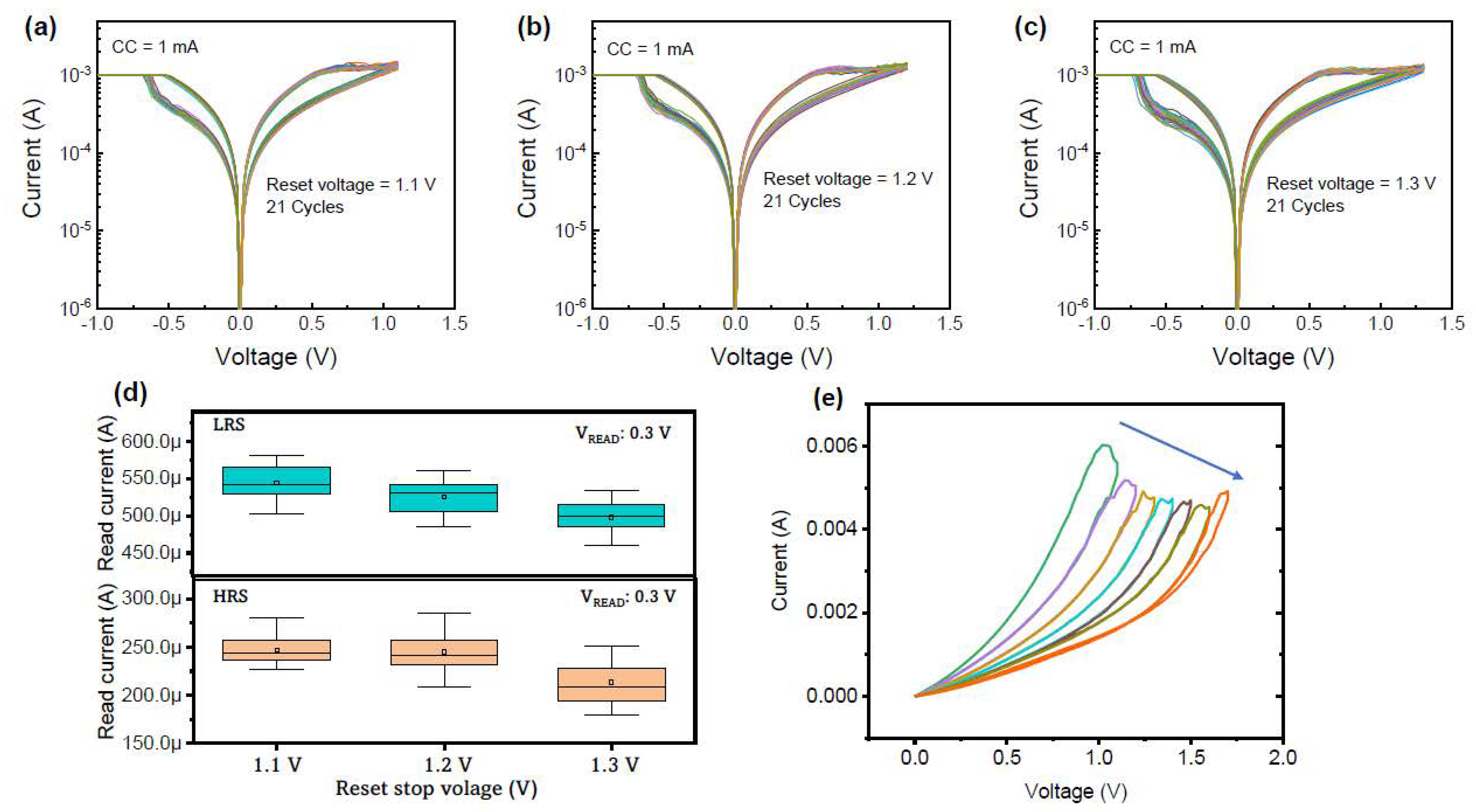
Next, we demonstrated the fine modulation of the LRS and HRS by varying the reset stop voltage. Figure 3a–c shows the I–V characteristics of the Pt/TiO2/HfAlOx/TiN device with reset stop voltages of 1.1 V, 1.2 V, and 1.3 V. Stable and uniform switching was observed for 21 cycles in each case. It can be noted that the LRS and HRS currents decreased with the increasing reset stop voltage in Figure 3d. The higher the voltage, the more the conducting filament ruptures, and thus, the HRS current decreases. It was also observed that the current gradually decreased as the reset stop voltage increased in the DC sweep mode, as shown in Figure 3e. However, MLC can be achieved by CC for the set process, which is not desirable for device control.
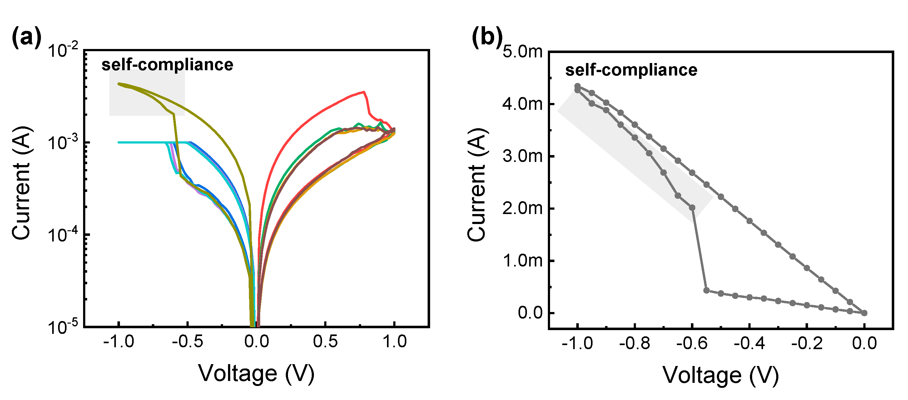
To overcome the limitation of the abrupt set process, we used different current regions in self-compliance for the gradual set process. Figure 4a shows the self-compliance curve after the CC controlled the I–V curves of the Pt/TiO2/HfAlOx/TiN device. The self-compliance region is clearly observed on the linear scale in Figure 4b. The current gradually increased with the voltage in the self-compliance region after an abrupt transition from 432.7 µA to 2 mA at −0.55 V. This gradual transition region is suitable for achieving MLC. The self-compliance behavior during the set transition due to the TiON layer acted as series resistance [43]. Furthermore, the gradual reset switching was maintained after the self-compliance set process.
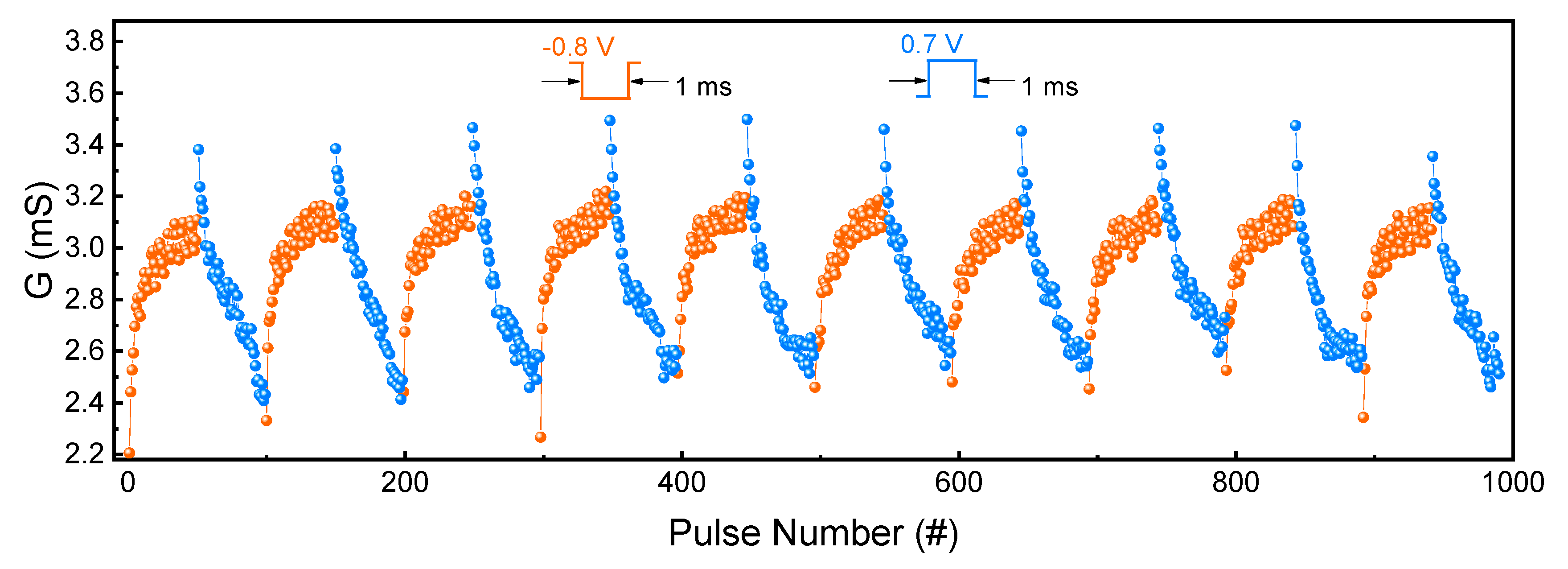
Next, the potentiation and depression characteristics were mimicked to apply the Pt/TiO2/HfAlOx/TiN device to a neuromorphic system. For potentiation, repetitive pulses with a voltage of −0.8 V and a width of 1 ms were used, as shown in Figure 5. Figure S1 shows the transient characteristics of the set and reset process. A low read pulse voltage (0.3 V) was used to not affect the conductance change during the reading. It should be noted that for gradual conductance modulation in the self-compliance region, we demonstrated 10 cycles of long-term potentiation and long-term depression, and found no significant degradation of the MLC.
4. Conclusions
In this study, multilevel cells were achieved in a Pt/TiO2/HfAlOx/TiN RRAM device by gradual resistive switching in the compliance region for neuromorphic system applications. The chemical and material characteristics of the TiO2/HfAlOx/TiN stack were confirmed by XPS depth profiling. The LRS was varied by the CC at a compliance current of 1 mA, and the HRS was accurately controlled by the reset stop voltage. Repetitive endurance and stable retention characteristics were observed in different compliance current modes. The self-compliance current region was used to improve the gradual resistive switching during the set process. Finally, stable and repetitive long-term potentiation and depression were obtained owing to the gradual resistive switching in the compliance current region for neuromorphic system applications.
Supplementary Materials
The following are available online at https://www.mdpi.com/article/10.3390/met11081199/s1. Figure S1: Transient characteristics of the set and reset processes.
Author Contributions
H.R. conducted the electrical measurements and wrote the manuscript. S.K. designed the experiment concept and supervised the study. All authors have read and agreed to the published version of the manuscript.
Funding
This work was supported by the Korea Institute of Energy Technology Evaluation and Planning (KETEP) and the Ministry of Trade, Industry and Energy (MOTIE) of the Republic of Korea (no. 20194030202320).
Conflicts of Interest
The authors declare no conflict interest.
References
- Lee, M.J.; Lee, C.B.; Lee, D.; Lee, S.R.; Chang, M.; Hur, J.H.; Kim, Y.B.; Kim, C.J.; Seo, D.H.; Seo, S.; et al. A fast, high endurance and scalable non-volatile memory device made from asymmetric Ta2O5−x/TaO2−x bilayer structures. Nat. Mater. 2011, 10, 625–630. [Google Scholar] [CrossRef]
- Waser, R.; Dittmann, R.; Staikov, G.; Szot, K. Redox-Based Resistive Switching Memories—Nanoionic Mechanisms, Prospects, and Challenges. Adv. Mater. 2009, 21, 2632–2663. [Google Scholar] [CrossRef]
- Russo, U.; Ielmini, D.; Cagli, C.; Lacaita, A.L. Self-Accelerated Thermal Dissolution Model for Reset Programming in Unipolar Resistive-Switching Memory (RRAM) Devices. IEEE Trans. Electron. Dev. 2009, 56, 193–200. [Google Scholar] [CrossRef]
- Banerjee, W.; Rahaman, S.Z.; Prakash, A.; Maikap, S. High-κ Al2O3/WOx Bilayer Dielectrics for Low-Power Resistive Switching Memory Applications. Jpn. J. Appl. Phys. 2011, 50, 10PH01. [Google Scholar] [CrossRef]
- Wu, M.C.; Lin, Y.-W.; Jang, W.-Y.; Lin, C.-H.; Tseng, T.-Y. Low-power and highly reliable multilevel operation in ZrO2 1T1R RRAM. IEEE Electron. Device Lett. 2011, 32, 1026–1028. [Google Scholar] [CrossRef]
- Wang, Y.; Liu, Q.; Long, S.; Wang, W.; Wang, Q.; Zhang, M.; Zhang, S.; Li, Y.; Zuo, Q.; Yang, J.; et al. Investigation of resistive switching in Cu-doped HfO2 thin film for multilevel non-volatile memory applications. Nanotechnology 2010, 21, 045202. [Google Scholar] [CrossRef]
- Ryu, H.; Choi, J.; Kim, S. Voltage Amplitude-Controlled Synaptic Plasticity from Complementary Resistive Switching in Alloying HfOx with AlOx-Based RRAM. Metals 2020, 10, 1410. [Google Scholar] [CrossRef]
- Prakash, A.; Jana, D.; Maikap, S. TaOx-based resistive switching memories: Prospective and challenges. Nanoscale Res. Lett. 2013, 8, 418. [Google Scholar] [CrossRef] [PubMed] [Green Version]
- Ryu, H.; Kim, S. Synaptic Characteristics from Homogeneous Resistive Switching in Pt/Al2O3/TiN Stack. Nanomaterials 2020, 10, 2055. [Google Scholar] [CrossRef] [PubMed]
- Yang, J.; Ryu, H.; Kim, S. Resistive and synaptic properties modulation by electroforming polarity in CMOS-compatible Cu/HfO2/Si device. Chaos Solitons Fractals 2021, 145, 110783. [Google Scholar] [CrossRef]
- Mahata, C.; Kim, S. Modified resistive switching performance by increasing Al concentration in HfO2 on transparent indium tin oxide electrode. Ceram. Int. 2021, 47, 1199–1207. [Google Scholar] [CrossRef]
- Ryu, H.; Kim, S. Irregular Resistive Switching Behaviors of Al2O3-Based Resistor with Cu Electrode. Metals 2021, 11, 653. [Google Scholar] [CrossRef]
- Chand, U.; Huang, K.C.; Huang, C.Y.; Tseng, T.Y. Mechanism of nonlinear switching in HfO2-based crossbar RRAM with inserting large bandgap tunneling barrier layer. IEEE Trans. Electron. Dev. 2015, 62, 3665–3670. [Google Scholar] [CrossRef]
- Chandrasekaran, S.; Simanjuntak, F.M.; Saminathan, S.; Panda, D.; Tseng, T.Y. Improving linearity by introducing Al in HfO2 as a memristor synapse device. Nanotechnology 2019, 30, 445205. [Google Scholar] [CrossRef]
- Chang, L.Y.; Simanjuntak, F.M.; Hsu, C.L.; Chandrasekaran, S.; Tseng, T.Y. Suboxide interface induced digital-to-analog switching transformation in all Ti-based memristor devices. Appl. Phys. Lett. 2020, 117, 073504. [Google Scholar] [CrossRef]
- Chen, S.; Noori, S.; Villena, M.A.; Shi, Y.; Han, T.; Zuo, Y.; Pedeferri, M.; Strukov, D.; Lanza, M.; Diamanti, V. Memristive Elecronic Synapses Made by Anodic Oxidation. Chem. Mater. 2019, 31, 8394–8401. [Google Scholar] [CrossRef]
- Zaffora, A.; Macaluso, R.; Habazaki, H.; Valov, I.; Santamaria, M. Electrochemically prepared oxides for resistive switching devices. Electrochim. Acta 2018, 274, 103–111. [Google Scholar] [CrossRef]
- Ryu, H.; Kim, S. Gradually Tunable Conductance in TiO2/Al2O3 Bilayer Resistors for Synaptic Device. Metals 2021, 11, 440. [Google Scholar] [CrossRef]
- Ryu, H.; Kim, S. Implementation of a reservoir computing system using the short-term effects of Pt/HfO2/TaOx/TiN memristors with self-rectification. Chaos Soliton. Fract. 2021, 150, 111223. [Google Scholar] [CrossRef]
- Ding, X.; Feng, Y.; Huang, P.; Liu, L.; Kang, J. Low-Power Resistive Switching Characteristic in HfO2/TiOx Bi-Layer Resistive Random-Access Memory. Nanoscale Res. Lett. 2019, 14, 157. [Google Scholar] [CrossRef] [Green Version]
- Ye, C.; Deng, T.; Zhang, J.; Shen, L.; He, P.; Wei, W.; Wang, H. Enhanced resistive switching performance for bilayer HfO2/TiO2 resistive random access memory. Semicond. Sci. Technol. 2016, 31, 105005. [Google Scholar] [CrossRef]
- Ryu, H.; Kim, S. Self-Rectifying Resistive Switching and Short-Term Memory Characteristics in Pt/HfO2/TaOx/TiN Artificial Synaptic Device. Nanomaterials 2020, 10, 2159. [Google Scholar] [CrossRef]
- George, S.M. Atomic Layer Deposition: An Overview. Chem. Rev. 2016, 110, 111–131. [Google Scholar] [CrossRef]
- Wang, I.T.; Chang, C.C.; Chiu, L.W.; Chou, T.; Hou, T.H. 3D Ta/TaOx/TiO2/Ti synaptic array and linearity tuning of weight update for hardware neural network applications. Nanotechnology 2016, 27, 365204. [Google Scholar] [CrossRef] [Green Version]
- Yang, J.J.; Strukov, D.B.; Stewart, D.R. Memristive devices for computing. Nat. Nanotechnol. 2013, 8, 13–24. [Google Scholar] [CrossRef]
- Jo, S.H.; Chang, T.; Ebong, I.; Bhadviya, B.B.; Mazumder, P.; Lu, W. Nanoscale memristor device as synapse in neuromorphic. Nano. Lett. 2010, 10, 1297–1301. [Google Scholar] [CrossRef]
- Cho, H.; Kim, S. Short-Term Memory Dynamics of TiN/Ti/TiO2/SiOx/Si Resistive Random Access Memory. Nanomaterials 2020, 10, 1821. [Google Scholar] [CrossRef] [PubMed]
- Cho, H.; Kim, S. Emulation of Biological Synapse Characteristics from Cu/AlN/TiN Conductive Bridge Random Access Memory. Nanomaterials 2020, 10, 1709. [Google Scholar] [CrossRef] [PubMed]
- Mikhaylov, A.; Pimashkin, A.; Pigareva, Y.; Gerasimova, S.; Gryaznov, E.; Shchanikov, S.; Zuev, A.; Talanov, M.; Lavrov, I.; Demin, V.; et al. Neurohybrid memristive CMOS-integrated systems for biosensors and neuroprosthetics. Front. Neurosci. 2020, 14, 358. [Google Scholar] [CrossRef] [PubMed]
- Surazhevsky, I.A.; Demin, V.A.; Ilyasov, A.I.; Emelyanov, A.V.; Nikiruy, K.E.; Rylkov, V.V.; Shchanikov, S.A.; Bordanov, I.A.; Gerasimova, S.A.; Guseinov, D.V.; et al. Noise-assisted persistence and recovery of memory state in a memristive spiking neuromorphic network. Chaos Solitons Fractals 2020, 146, 110890. [Google Scholar] [CrossRef]
- Ismail, M.; Kim, S. Negative differential resistance effect and dual bipolar resistive switching properties in a transparent Ce-based devices with opposite forming polarity. Appl. Surf. Sci. 2020, 530, 147284. [Google Scholar] [CrossRef]
- Kim, S.; Abbas, Y.; Jeon, Y.R.; Sergeevich, A.; Ku, B.; Choi, C. Engineering synaptic characteristics of TaOx/HfO2 bi-layered resistive switching device. Nanotechnology 2018, 29, 415204. [Google Scholar] [CrossRef]
- Kim, S.; Park, B.G. Nonlinear and multilevel resistive switching memory in Ni/Si3N4/Al2O3/TiN structures. Appl. Phys. Lett. 2016, 108, 212103. [Google Scholar] [CrossRef]
- Sokolov, A.S.; Son, S.K.; Lim, D.; Han, H.H.; Jeon, Y.R.; Lee, J.H.; Choi, C. Comparative study of Al2O3, HfO2, and HfAlOx for improved self-compliance bipolar resistive switching. J. Am. Ceram. Soc. 2017, 100, 5638–5648. [Google Scholar] [CrossRef]
- Zazpe, R.; Ungureanu, M.; Golmar, F.; Stoliar, P.; Llopis, R.; Casanova, F.; Pickup, D.F.; Rogero, C.; Hueso, L.E. Resistive switching dependence on atomic layer deposition parameters in HfO2-based memory devices. J. Mater. Chem. C 2014, 2, 3204–3211. [Google Scholar] [CrossRef]
- Bharti, B.; Kumar, S.; Lee, H.-N.; Kumar, R. Formation of oxygen vacancies and Ti3+ state in TiO2 thin film and enhanced optical properties by air plasma treatment. Sci. Rep. 2016, 6, 32355. [Google Scholar] [CrossRef] [PubMed]
- Rahmani, M.K.; Ismail, M.; Mahata, C.; Kim, S. Effect of interlayer on resistive switching properties of SnO2-based memristor for synaptic application. Res. Phys. 2020, 18, 103325. [Google Scholar] [CrossRef]
- Lin, K.L.; Hou, T.H.; Shieh, J.; Lin, J.H.; Chou, C.T.; Lee, Y.J. Electrode dependence of filament formation in HfO2 resistive-switching memory. J. Appl. Phys. 2011, 109, 084104. [Google Scholar] [CrossRef] [Green Version]
- Privitera, S.; Bersuker, G.; Butcher, B.; Kalantarian, A.; Lombardo, S.; Bongiorno, C.; Geer, R.; Gilmer, D.C.; Kirsch, P.D. Microscopy study of the conductive filament in HfO2 resistive switching memory devices. Microelectron. Eng. 2013, 109, 75–78. [Google Scholar] [CrossRef]
- Zhang, R.; Huang, H.; Xia, Q.; Ye, C.; Wei, X.; Wang, J.; Zhang, L.; Qiang, L.; Zhu, Q. Role of Oxygen Vacancies at the TiO2/HfO2 Interface in Flexible Oxide-Based Resistive Switching Memory. Adv. Electron. Mater. 2019, 5, 1800833. [Google Scholar] [CrossRef]
- Lee, D.Y.; Tsai, T.L.; Tseng, T.Y. Unipolar resistive switching behavior in Pt/HfO2/TiN device with inserting ZrO2 layer and its 1 diode-1 resistor characteristics. Appl. Phys. Lett. 2013, 103, 032905. [Google Scholar] [CrossRef] [Green Version]
- Zhang, W.; Kong, J.-Z.; Cao, Z.-Y.; Li, A.-D.; Wang, L.-G.; Zhu, L.; Li, X.; Cao, Y.-Q.; Wu, D. Bipolar Resistive Switching Characteristics of HfO2/TiO2/HfO2 Trilayer-Structure RRAM Devices on Pt and TiN-Coated Substrates Fabricated by Atomic Layer Deposition. Nanoscale Res. Lett. 2017, 12, 2735. [Google Scholar] [CrossRef] [PubMed]
- Jeon, H.; Park, J.; Jang, W.; Kim, H.; Kang, C.; Song, H.; Kim, H.; Seo, H.; Jeon, H. Stabilized resistive switching behaviors of a Pt/TaOx/TiN RRAM under different oxygen contents. Phys. Status Solidi A 2014, 211, 2189–2194. [Google Scholar] [CrossRef]
Figure 1.
(a) Schematic of the Pt/TiO2/HfAlOx/TiN device. XPS spectra of the TiO2/HfAlOx/TiN stack: (b) Ti 1p for Ti-O bonds, (c) Ti 1p for Ti-N bonds, (d) Hf 4f, and (e) Al 2p spectra.
Figure 1.
(a) Schematic of the Pt/TiO2/HfAlOx/TiN device. XPS spectra of the TiO2/HfAlOx/TiN stack: (b) Ti 1p for Ti-O bonds, (c) Ti 1p for Ti-N bonds, (d) Hf 4f, and (e) Al 2p spectra.

Figure 2.
(a) I–V characteristics of the Pt/TiO2/HfAlOx/TiN RRAM device. (b) Endurance at a compliance current (CC) of 1 mA in the high-resistance state (HRS) and low-resistance state (LRS). (c) Endurance at a CC of 10 mA. (d) Retention characteristics for 3600 s.
Figure 2.
(a) I–V characteristics of the Pt/TiO2/HfAlOx/TiN RRAM device. (b) Endurance at a compliance current (CC) of 1 mA in the high-resistance state (HRS) and low-resistance state (LRS). (c) Endurance at a CC of 10 mA. (d) Retention characteristics for 3600 s.

Figure 3.
I–V characteristics of the Pt/TiO2/HfAlOx/TiN RRAM device at reset stop voltages of (a) 1.1 V, (b) 1.2 V, and (c) 1.3 V. (d) Read current distribution as a function of reset stop voltage. (e) MLC by reset stop voltage.
Figure 3.
I–V characteristics of the Pt/TiO2/HfAlOx/TiN RRAM device at reset stop voltages of (a) 1.1 V, (b) 1.2 V, and (c) 1.3 V. (d) Read current distribution as a function of reset stop voltage. (e) MLC by reset stop voltage.

Figure 4.
Self-compliance characteristics of the Pt/TiO2/HfAlOx/TiN RRAM device: (a) log-scale; (b) linear scale.
Figure 4.
Self-compliance characteristics of the Pt/TiO2/HfAlOx/TiN RRAM device: (a) log-scale; (b) linear scale.

Figure 5.
Potentiation and depression characteristics of the Pt/TiO2/HfAlOx/TiN RRAM device.

Publisher’s Note: MDPI stays neutral with regard to jurisdictional claims in published maps and institutional affiliations. |
© 2021 by the authors. Licensee MDPI, Basel, Switzerland. This article is an open access article distributed under the terms and conditions of the Creative Commons Attribution (CC BY) license (https://creativecommons.org/licenses/by/4.0/).
Share and Cite
MDPI and ACS Style
Ryu, H.; Kim, S. Gradually Modified Conductance in the Self-Compliance Region of an Atomic-Layer-Deposited Pt/TiO2/HfAlOx/TiN RRAM Device. Metals 2021, 11, 1199. https://doi.org/10.3390/met11081199
AMA Style
Ryu H, Kim S. Gradually Modified Conductance in the Self-Compliance Region of an Atomic-Layer-Deposited Pt/TiO2/HfAlOx/TiN RRAM Device. Metals. 2021; 11(8):1199. https://doi.org/10.3390/met11081199
Chicago/Turabian StyleRyu, Hojeong, and Sungjun Kim. 2021. "Gradually Modified Conductance in the Self-Compliance Region of an Atomic-Layer-Deposited Pt/TiO2/HfAlOx/TiN RRAM Device" Metals 11, no. 8: 1199. https://doi.org/10.3390/met11081199
Note that from the first issue of 2016, this journal uses article numbers instead of page numbers. See further details here.