

Abstract
We report uniaxially oriented nickel aluminum (NiAl) films grown by DC magnetron sputtering under in situ heating. The films self-organize in (110) orientation with relatively low surface roughness and tight grain boundaries in columnar structure. The electrical carrier concentration and resistivity are on the order of 1021 cm−3 and 10−5 Ω · cm, respectively. The plasmonic performance, as indicated by the dielectric function, is comparable to that of a NiAl single crystal and exceeds those of conventional refractory materials (molybdenum, tungsten, titanium nitride) at visible to NIR wavelengths. This work paves the way to superalloy-based plasmonic nanostructures for photothermal energy applications.
Export citation and abstract BibTeX RIS
The use of refractory materials such as molybdenum, 1) tungsten, 2) titanium nitride (TiN), 3) or lanthanum hexaboride (LaB6), 4) in high-temperature plasmonic applications has been proposed. However, these materials are severely oxidized at high temperatures in air. Nickel-based superalloys containing Ti, Ta, and W are used in a base material for turbine blades or turbine vanes in jet engines with surface oxide coating on a base material to inhibit further oxidation and heating. 5) In this context, intermetallic nickel aluminum (NiAl) can be a promising candidate with the advantages of a high melting point, 6) extreme hardness, a low density (5.90 g cm−3), 7) and high thermal/electrical conductivity. In particular, because of its excellent oxidation resistance resulting from the formation of a protecting alumina layer on the NiAl surface, this material is sufficiently robust against oxidation at elevated temperature in air. 8) Consequently, NiAl is a desirable material for practical high-temperature energy applications.
Although the growth of high-quality NiAl single crystals is well-established, 9) research on lower-dimensional materials is needed to obtain high-crystallinity or epitaxial thin films with the optimal surface orientation. Research on NiAl has extended to various configurations, such as shape memory alloy thin films, 10) and hybrid materials in which NiAl can serve as an underlayer. 11) Various techniques have been used to synthesize NiAl films, including magnetron sputtering, 12) electron beam evaporation, 13) chemical vapor deposition, 14) and molecular beam epitaxy. 15) Sputter deposition is highly feasible owing to its CMOS compatibility, versatile controllability, and suitability for mass production. However, previous reports reveal the main drawback of non-stoichiometric films, as aluminum and nickel sources were deposited separately, and non-uniform multilayer films with a Nix Aly component ratio of x ≠ y ≠ 1 were produced. Here, we report the stoichiometric and uniaxial growth on silicon substrates of NiAl thin films sputtered from a single NiAl alloy target at elevated temperatures (≥744 K). The structure, morphology, and electrical and optical properties of the NiAl films are discussed in the context of optical applications at high temperatures. Among superalloys, NiAl has a rather high melting temperature and is more difficult to grow as bulk highly-oriented crystals. However, as thin films, our study demonstrates a method of preparing high-crystallinity uniaxial NiAl thin films at temperatures well below its melting point of 1911 K; these films have optical properties comparable to those of single crystals. This method will open a wide variety of practical applications, especially photothermal applications such as radiative heating and photothermal catalysis at high temperatures.
NiAl films were deposited from a commercial NiAl alloy target (99.9%, Furuuchi Chemical, Japan) on silicon(100) substrates by a sputtering apparatus (i-Miller, Shibaura Mechatronics Corporation). The silicon substrates were ultrasonically cleaned with acetone, ethanol, and isopropyl alcohol sequentially for 5 min each. The base pressure in the sputtering chamber was approximately 2.5 × 10⁻⁵ Pa, and the sputtering power was 200 W. High-purity argon gas (20 m3 s−1) was introduced into the chamber to obtain a working pressure of 0.51 Pa. The deposition temperature was varied from room temperature (298 K) to 967 K.
The crystallographic information of the NiAl films was obtained using X-ray diffraction (XRD, SmartLab, Rigaku, Japan) with Cu Kα radiation (λ = 1.5425 Å). The film surface morphology and roughness were examined by scanning electron microscopy (SEM, SU-4800, Hitachi High-Technologies, Japan) and atomic force microscopy (AFM, Multimode Nanoscope IIIA, Bruker, US) in tapping mode using a Si cantilever (SI-DF20, Hitachi Hightech). Complex permittivity values from the UV to NIR (0.3–3.5 μm) were obtained by spectroscopic ellipsometry (SE 850 DUV, SENTECH, Germany) using a Drude–Lorentz model with three Lorentz oscillators for all the fittings. The carrier mobility, concentration, and film resistivity were determined by Hall measurements (Resitest 8400 series, TOYO, Japan).
NiAl alloy has bcc structure with a lattice constant of 2.88 Å (CsCl-type lattice, space group Pm-3m), where the aluminum atom is located at the center of the unit cell, and nickel atoms appear at the corners. 16) Figure 1 shows the XRD patterns of NiAl films deposited at temperatures ranging from 298 to 967 K. All the samples had cubic structure with space group Pm-3m (PDF #44-1187). NiAl samples prepared at room temperature exhibited two preferred orientations, (100) and (110). However, as the deposition temperature increased from 744 to 967 K, the diffraction patterns showed a predominant sharp peak with (110) orientation at 2θ ≈ 44.7°, which is similar to that of a (110)-cut single crystal reference sample. Furthermore, four additional small peaks corresponding to (100), (111), (200), and (210) orientations appeared at 31.2°, 55.5°, 65.0°, and 73.9°, respectively. At room temperature, NiAl has an intrinsic high antiphase boundary energy. In both the polycrystalline and single crystal forms, the (100) orientation is considered to be a hard orientation, whereas the (110) orientation is considered a soft orientation. The predominant initial orientation of this compound is (100), and other orientations are energetically less favorable at room temperature. Higher deposition temperatures promote mass transport and accommodate stress; thus, they may increase the entropy term in the free energy owing to slight disorder at grain boundaries associated with the presence of other minor orientations. 17)

Fig. 1. (Color online) XRD patterns of NiAl films on Si (100) substrates at different temperatures. Standard diffraction pattern of NiAl (PDF#44-1188) at the bottom. Inset: unit cell of NiAl with an aluminum atom at the center and surrounding nickel atoms. Diffraction pattern from a (110)-cut single crystal NiAl is also placed for comparison.
Download figure:
Standard image High-resolution imageFigure 2 shows the surface morphology of the NiAl films. All the films exhibit a continuous and closed morphology on the Si(100) substrate. As the deposition temperature increased to 744 K, the grain size increased and the film morphology remained continuous. Higher temperatures up to 889 K promoted better crystallinity and grain growth. At 889 K, small grains coalesced to form larger grains with very small gaps between them, which introduced surface porosity and increased the surface roughness. The separation between grains become more obvious at 967 K. During crystal growth at this temperature, tiny pores were created, and the formation and expansion of secondary grains were promoted, resulting in increased pressure at grain boundaries. The average grain size was calculated from the XRD patterns using the Scherrer equation. Porous morphology with large grains assembled from smaller grains was observed [Fig. 2(e)]. 18) From room temperature to 744 K, the grain size clearly increased. At elevated temperatures, the morphology changed dramatically, especially at 889 K, where the grain size reached a maximum value of 25.7 nm; thus, NiAl film prepared at this temperature had the highest crystallinity.

Fig. 2. SEM images of NiAl films sputtered at (a) room temperature (grain size 12.2 nm), (b) 744 K (grain size 21.4 nm), (c) 814 K (grain size 20.4 nm), (d) 889 K (grain size 25.7 nm) and (e) 967 K (grain size 23.5 nm) on silicon substrates. Grain size was taken from the XRD analysis showing reasonable agreement with the SEM result.
Download figure:
Standard image High-resolution imageFigure 3 shows AFM images of the surface morphologies of NiAl films deposited at 744, 814, and 889 K. The root mean square roughness (Rrms) of these samples was determined to be 6.7, 10.0, and 13.1 nm, respectively, and shows the same trend as the XRD and SEM results.

Fig. 3. (Color online) AFM images of NiAl films deposited at various temperatures: (a), (d) 744 K (Rrms = 6.7 nm); (b), (e) 814 K (Rrms = 10.0 nm); (c), (f) 889 K (Rrms = 13.1 nm) on Si substrates displayed in two-dimensional (above) and three-dimensional (below) styles.
Download figure:
Standard image High-resolution imageThe electrical properties of the NiAl films were characterized by Hall measurement at room temperature (Fig. 4). The Hall mobility increased gradually with increasing substrate temperature from 298 K (10.9 cm2 V−1 · s−1) to 814 K (30.6 cm2 V−1 · s−1); it reached a maximum value at 889 K (45.2 cm2 V−1 · s−1) and decreased sharply at 967 K (20.7 cm2 V−1 · s−1). This behavior indicates enhanced crystallinity, larger grains, and less electron scattering at grain boundaries/defects with increasing temperature. All the sputtered NiAl films had high carrier densities of ∼1021 cm−3. At elevated temperatures, the dense fine columnar structure was transformed to wider columns along grain boundaries, and the electron mobility varied with the grain size in the columns. Columnar NiAl films wider grain boundaries have higher electron mobility than dense fine columnar films. The reason could be the larger grain size of films with columns aligned nearly in the preferential (110) direction, which minimizes carrier scattering under DC current flow, resulting in higher mobility and a better optical response of the film. By contrast, the carrier concentration tended to decrease with increasing growth temperature; it had a minimum value at 889 K (5.17 × 1021 cm−3) and increased at 967 K (9.52 × 1021 cm−3), indicating considerable mass rearrangement and a transition to a porous and roughened surface morphology, which might lead to the underestimated carrier density in the Hall measurement. Owing to these changes, as a whole the electrical resistivity decreased as the temperature increased, reaching a minimum (2.67 × 10⁻⁵ Ω · cm) at 889 K. The resistivity was calculated from the mobility and carrier concentration results using the formula in Fig. 4(b). The resistivity decreased by a factor of approximately two as the film thickness increased from 20 nm (5.85 × 10⁻⁵ Ω · cm) to 100 nm (2.67 × 10⁻⁵ Ω · cm) and was approximately 2.5 × 10⁻⁵ Ω · cm for thicker films. The resistivity ρ, carrier concentration n, and mobility μ are related as ρ = 1/nqμ, and as shown in Fig. 4(b), resistivity and mobility show stronger correlation compared with the carrier concentration. As the film growth proceeds beyond a thickness of 20 nm under heating, the connectivity of the film becomes sufficiently high, and the resistivity drops thereafter. In addition, the grains remain tightly packed and stay connected by suppressing the dewetting of the film. Consequently, free electrons can travel easily from grain to grain, dramatically increasing the film mobility. Furthermore, as the film thickness increased, the surface scattering effect decreased and the electron scattering path length increased, decreasing the film resistivity. 19) By contrast, the decrease in mobility at a deposition temperature of 967 K is ascribed to the increased porosity and surface roughness of the film.
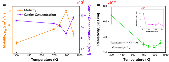
Fig. 4. (Color online) Hall measurement results of NiAl films at different deposition conditions. (a) Mobility and carrier concentration versus growth temperature, and (b) resistivity versus growth temperature, and effect of film thickness on the resistivity.
Download figure:
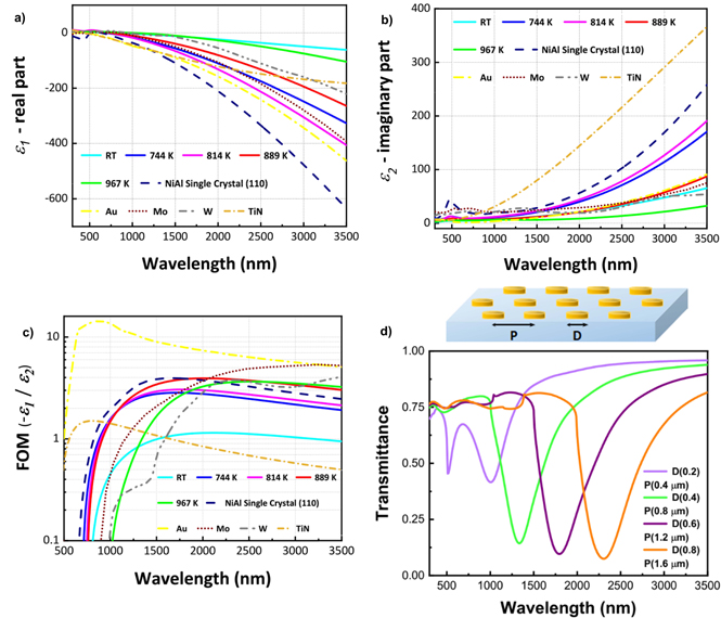
Standard image High-resolution imageThe dielectric functions (permittivities) of the NiAl films were obtained by spectroscopic ellipsometry at wavelengths of 300–3500 nm (Fig. 5). All the samples exhibited crossover points (ε1 = 0) between 586 and 750 nm. The films behaved as dielectric materials in the UV–vis region and exhibited strong metallicity from the NIR to the mid-infrared region. Furthermore, the metallicity increased with increasing deposition temperature, indicating increased free carrier mobility, in good agreement with the Hall measurements. For comparison, the permittivities of the sputtered NiAl films, a NiAl single crystal, and other refractory metals are plotted in Fig. 5. Figure 5(a) clearly shows that the real part ε1 of the permittivity of the films approached single crystal values (that is, the films became more metallic) as the deposition temperature increased. Interestingly, the permittivity of the NiAl film sputtered at 814 K was comparable to that of gold, 20) and better than those of the commonly used materials Mo, 21) W, 22) and TiN. 3) The imaginary part ε2 of the complex permittivity of the sputtered films was lower (indicating less loss) than those of the single crystal, which could be ascribed to the presence of undefined particles seen in SEM on the polished surface (most possibly polishing powders) which causes some carrier scattering. The figure of merit (FOM), −ε1/ε2, which indicates the suitability for use as a plasmonic material, is plotted in Fig. 5(c) for comparison with Au as a standard reference. The FOM of the NiAl film sputtered at room temperature is low, mainly because of the low metallicity (poor carrier mobility). The films prepared at 744 and 814 K have higher FOMs than the typical refractory materials Mo and W up to 2000 nm and a much higher FOM than TiN. The NiAl film sputtered at 889 K had the highest FOM, which was quite close to that of the NiAl single crystal at approximately 2000 nm and even slightly higher than that at longer wavelengths. Consequently, the as-grown NiAl films exhibited a larger plasmonic response than conventional refractory materials (Mo, W, and TiN). Figure 5(d) represents the electromagnetic simulation (calculated using the RCWA method, Synopsys' RSoft) of NiAl-based nanostructure to examine the properties of localized surface plasmon resonance. The complex permittivity of NiAl film used for this simulation was derived from the film sputtered at 889 K. NiAl nanodisks were modeled in a hexagonal lattice on a glass substrate, and the disk diameter (D) is varied from 0.2 to 0.8 μm. The periodicity P was set as P = 2D. The thickness of the NiAl nanodisks was fixed at 50 nm. Well defined resonant absorption (dips in the transmission spectra) were seen, and by changing the disk diameter, the resonant wavelength shifts from visible to the near-infrared region. These results indicate that NiAl disks will function as plasmon polariton resonators in the NIR region, which are highly suitable for heat/electricity transducers, for example, such as for IR thermal emitters, photothermal heaters/catalysts, and photodetectors. 23–26)
Fig. 5. (Color online) Comparison of the measured complex permittivities and figure of merit (FOM) −ε1 /ε2 of the NiAl films deposited at different temperatures of deposition against NiAl single crystal, Au, W, Mo, and TiN. (a) Real part; (b) imaginary part and (c) FOM. (d) Simulated transmittance spectra of circular NiAl disks arranged in hexagonal arrays on a glass substrate. The diameter D of the disks and the periodicity P of the arrays are varied from 0.2–0.8 μm to 0.4–1.6 μm, respectively, while NiAl thickness is fixed at 50 nm.
Download figure:
Standard image High-resolution image
In summary, the growth of high-quality NiAl film by magnetron sputtering from a single NiAl target under in situ heating at temperatures ranging from room temperature to 967 K was reported. All the films exhibited intense, sharp peaks indicating the preferred (110) orientation with columnar grains. High carrier concentrations of ∼1021 cm−3 and a minimum resistivity of 2.67 × 10⁻⁵ Ω · cm were obtained. The optical FOMs of the NiAl films indicated better performance than the commonly used refractory optical materials, molybdenum, tungsten, and titanium nitride, indicating their strong potential for use as photothermal converters. Surprisingly, the FOM of the (110)-oriented NiAl film deposited at 889 K was nearly comparable to that of a NiAl single crystal from the visible to the NIR region and even higher at longer wavelengths. We believe that the NiAl (110) films reported here could be a material of choice for various NiAl-based refractory photonic applications.
Acknowledgments
We appreciate the technical assistance provided by N. Furuhata. This work was initiated and partially supported by JSPS KAKENHI (16H06364) and CREST "Phase Interface Science for Highly Efficient Energy Utilization" (JPMJCR13C3), Japan Science and Technology Agency.