Optical Absorption and Reflectivity of Four 2D Materials: MoS2, MoP2, NbS2, and NbP2
 E. Garcés
 O. Salas2
  L. F. Magaña
- 1Instituto de Física, Universidad Nacional de México, México City, Mexico
- 2Escuela Superior de Ingeniería Mecánica y Eléctrica, Instituto Politécnico Nacional, Avenida Instituto Politécnico Nacional S/N, México City, Mexico
We calculated the energy band structure and the optical absorption and reflectivity for each of the ultrathin 2D hexagonal materials MoS2, MoP2, NbS2, and NbP2. Our simulations included density functional theory, generalized gradient approximation (GGA), and the Quantum Espresso code. Other researchers already synthesized the first three materials. We obtained that NbP2 should be another hexagonal 2D material. In all cases in the infrared and visible ranges, the absorptions present much larger concerning graphene. However, the absorptions for MoP2, NbP2, and NbS2, are far more prominent concerning MoS2. In the ultraviolet region, the absorptions are like each other and differ from graphene. In all cases, the reflectivities are similar to each other and vary from graphene.
Introduction
Graphite is a layered material with strong bonds between atoms of the same layer and a much weaker interaction between particles of different layers, basically Van der Waals type interactions among layers. The experimental obtention of a graphite monolayer (i.e., what we know today as graphene) was only theoretical speculation since 1968 when Mermin (1968) proved that one and two-dimensional materials could within the harmonic approximation not exist naturally. However, in 2004 Novoselov and Geim isolated the first 2D material, graphene (Novoselov et al., 2004). They deserved the Nobel Prize in 2010. Nevertheless, we must say that the careful investigation of graphene shows the presence of ruffles, ripples (Fasolino et al., 2007; Meyer et al., 2007) that make graphene strictly a 3D material. In this way, the theoretical theorem about 2D materials holds still.
Today, clearly layered compounds, i.e., materials that show a strong bonding in a plane and a weak van der Waals interaction between layers, are excellent candidates to produce 2D materials. As examples of these materials, we can mention chalcogenides, halides, nitrides, hydrides, clays, carbides, and layered oxides. We have, among them, metals, insulators, superconductors, semimetals, and semiconductors. Notice that the one-layer obtained from these materials is not atomically thin, so they are three-dimensional strictly speaking (Brivio et al., 2011; Miró et al., 2013). We may call them ultra-thin 2D materials.
The spectrum of design and applications of nanodevices has enlarged rapidly with the layered ultra-thin 2D materials. It is clear at present that graphene is only one of an expanding 2D materials Universe. In particular, the transition metal dichalcogenides attract much research today. The molecules of these materials form layers with weak interaction with each other by van der Walls-type forces. Their symmetry is hexagonal or rhombohedral (Ganatra and Zhang, 2014; Miró et al., 2014; Das et al., 2015).
The presence of these materials gives excellent support to the development of flexible devices, optoelectronics, and nanoelectronics. This fact is due to their electronic properties. Among these materials, we find insulators, semiconductors, metals, semimetals, and superconductors. Moreover, we see band gaps, direct and indirect, and imply radiation from infrared to ultraviolet. Therefore, investigating these materials’ electronic and optical properties is necessary to use them (Ganatra and Zhang, 2014; Miró et al., 2014; Das et al., 2015).
Ultra-thin 2D MoS2 is a semiconductor with various possible applications in optoelectronics, nanoelectronics, and flexible devices (Ganatra and Zhang, 2014; Miró et al., 2014; Pan, 2014; Schaak, 2014; Das et al., 2015). NbS2 is a metallic material, superconductor (Kačmarčík et al., 2010). Furthermore, ultrathin NbS2 is a nonlinear optical helpful material in optoelectronic devices (Maldonado et al., 2020). 2D MoP2 is a material used as an abrasive and possible catalyst in crude oil hydro-processing (Soto et al., 2004). Furthermore, it is utilized for efficient electrocatalytic hydrogen evolution (Gao et al., 2018). We know a report on the structure of bulk NbP2 from almost six decades ago (Hullinger, 1964) and work on its electronic properties (Elkana Kipkogei Rugut, 2017). However, to our knowledge, there is no empirical evidence of 2D NbP2.
Materials and Methods
We used density functional theory, generalized gradient approximation (GGA), and the Quantum Espresso code to optimize the ultrathin materials MoS2, NbS2, MoP2, and NbP2. We calculated the band structure and the optical absorption and reflectivity of these 2D materials and compared them to each other and graphene.
We obtained the optimized configurations of graphene and each of the four ultra-thin 2D materials MoS2, MoP2, NbS2, NbP2. We employed density functional theory with the Quantum Espresso code (Giannozi et al., 2009). Given that the systems we are investigating are not magnetic, we did not perform relativistic nor spin-polarized simulations; we used the norm-conserving Troullier–Martins pseudopotentials (Troullier and Martins, 1991) and the Perdew-Burke-Ernzerhof (PBE) approximation for generalized gradient approximation (GGA) (Perdew et al., 1996). We considered 50 k points within the Monkhorst–Pack k point scheme (Monkhorst and Pack, 1976), and we took cut-off energy of 1,000 eV. For the threshold value for convergence, we chose 1.0 × 10⁻⁶ eV. We used periodic conditions and an initial hexagonal unit cell to perform our simulations with a = b = 3.189 Å, c = 25 Å. The magnitude of c is large enough to avoid inconvenient interactions between the surfaces of adjacent cells. There are 18 atoms in the unit cell (nine metallic and nine non-metallic). We validated our pseudopotentials for C, Mo, S, P, and Nb, from the optimized configurations, obtaining corresponding bond lengths. In this manner, we found for graphene a C-C bond size of 1.419 Å, which is in good agreement with an experimental value of 1.421 Å (Gmelin Handbuch Der Anorg, 1968). For MoS2, we got 2.4140 Å for the Mo-S bonding compared to 2.41 Å (Joensen et al., 1986). In the case of MoP2, we obtained the Mo-P bond length 2.4835 Å that compares well with the observed value of 2.5 Å (Wu et al., 2016). For NbS2, we calculated 2.4473 Å for the Nb-S bonding compared to 2.473 Å (Morosin, 1974). To visualize the calculated configurations, we used the XCrySDen software (Kokalj, 1999).
We employed the modified Bloch tetrahedron for integration in the first Brillouin zone (Blöch et al., 1994) and calculated the band energy structure. From this, we obtained the dielectric tensor and the optical absorption and reflectivity.
In the limit of the linear optics and using the random phase approximation (RPA) (Kumar et al., 2008), the imaginary part of the dielectric tensor
Here ω is the photon frequency, n is the electron density, and m is the effective mass. The indices α and β are the cartesian components of p that is the vector defining the incident electric field’s polarization. The symbols ck and νk are the wave functions corresponding to the conduction, and the valence bands with crystal wave vector k;fc is the Fermi distribution function for the state c. The sum of the transitions from occupied to unoccupied states is over the first Brillouin zone. Finally, we weigh the probability of a change.
By the Kramers-Kronig relations (Kittel, 1966) and using Eq. 1
In Eq. 2, P denotes the principal value. We take a normal incidence of the electromagnetic wave; thus, the reflectivity and absorption Rii and Aii are (with n and k being the refractive index and extinction coefficient, respectively):
And
Results
We performed our simulations with density functional theory to optimize the geometry of graphene and four ultra-thin 2D materials for comparison. We calculated the energy band structure and the optical absorption and reflectivity of each one of them.
In Figure 1, we show the optimized structures for graphene and the other materials. To our knowledge, there is not an empirical report of 2D NbP2. Thus, we tested the stability of this predicted material. We optimized this structure utilizing a first-principles molecular dynamics (FPMD) simulation at 300 K and atmospheric pressure. The calculation includes all the vibrations, rotations, velocities of each particle, and interactions in this method. Of course, this is for every particle of the whole system. See references (Payne et al., 1992; Marx and Grotendorst, 2000; Frenkel and Smit, 2001; Marx and Hutter, 2009) for more details of FPMD. We obtained the same final structure for 2D NbP2. Thus, we show that it is dynamically stable at 300 K and atmospheric pressure. We present in Figure 2 the evolution of the system towards equilibrium with time after 1,600 femtoseconds.
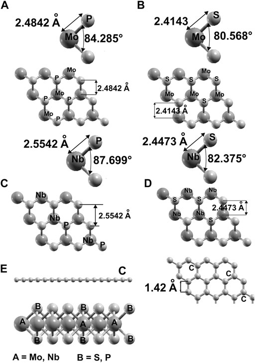
FIGURE 1. We present the result of our optimization for the structures we considered. For MoP2: (A); for MoS2: (B); for NbP2: (C), for NbS2: (D). In (E) we show top and side views for graphene and the side view of the other materials.
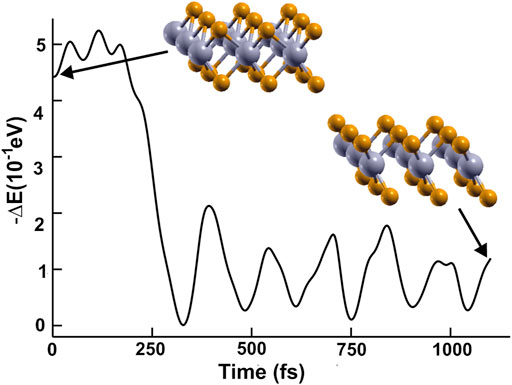
FIGURE 2. We present the evolution of the system towards equilibrium using FPMD at 300 K and atmospheric pressure.
In Figures 3, 4, we show the density of states (DOS) and the projected density of states (PDOS) of the four ultra-thin 2D materials we consider. In Figure 3A, we notice the hybridization of orbitals s from sulfur and p from molybdenum below the Fermi Energy. Notice in Figure 3B the hybridization of orbitals p from phosphorus and d from molybdenum around the Fermi energy. From Figure 4A, we notice the hybridization of orbitals s (with a small contribution) and p from sulfur, and orbitals p and d from niobium around the Fermi energy. In Figure 4B, we notice the hybridization of orbitals s and p from phosphorus and orbitals p and d from niobium around the Fermi energy.
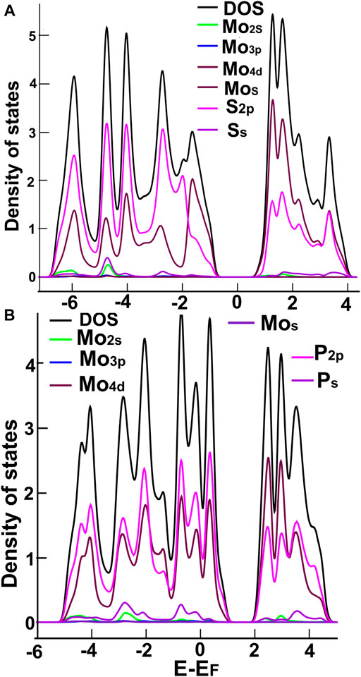
FIGURE 3. We show the DOS and PDOS para MoS2 (A) and MoP2 (B).
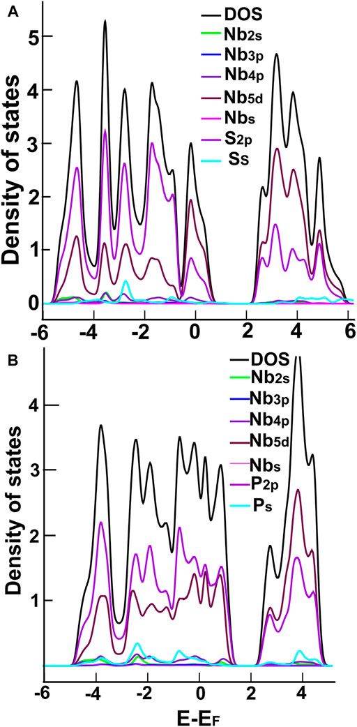
FIGURE 4. We show the DOS and PDOS para NbS2 (A) NbP2 (B).
Energy Band Structures
In Figures 5–7, we show our calculations for the band structure for graphene, MoS2, MoP2, NbS2, and NbP2, respectively.
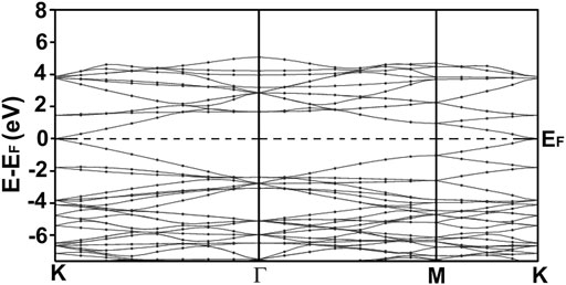
FIGURE 5. We present our calculated band structure for graphene. Our calculation agrees with other results reported in the literature (Novoselov et al., 2005; Wu et al., 2016). Notice the Dirac cones at the K points. Graphene is a non-typical semiconductor with a zero-gap.
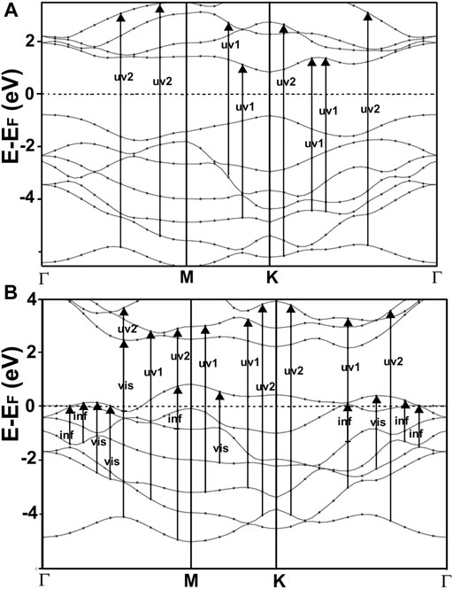
FIGURE 6. We show our result for the band structure of MoS2(A) and MoP2(B). For MoS2, the gap is at the K point, and it has a value of 1.714 eV. This value and the general features of the band structure agree with reports from other authors (Novoselov et al., 2004; Ganatra and Zhang, 2014). In the case of MoP2, Notice the two bands that cross several times the Fermi energy, indicating that this is a metallic material. To our knowledge, there is no other calculation of the band structure for MoP2 reported in the literature.
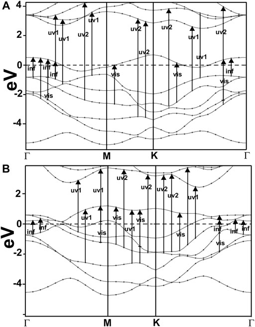
FIGURE 7. We show our result for the band structure of NbS2(A) and NbP2(B). For NbS2, notice the band crossing several times at the Fermi level, indicating a metallic material. These results agree with the works of other authors (Mermin, 1968; Miró et al., 2014). In the case of NbP2, we can see several bands crossing the Fermi level, too, and thus, it is a metallic material.
Figure 5 shows our calculation of the energy band structure for graphene. We can notice the Dirac points at the K points. Our results agree with other author’s reports (Novoselov et al., 2005). Graphene is a strange semiconductor with a zero bandgap and interesting and peculiar electronic properties.
In Figure 6A, we present our calculated band structure for MoS2. This material has a typical semiconductor bandstructure; it shows a gap of 1.714 eV at the K point. The width of the opening and the general features of the band structure agree with reports from other authors (Ganatra and Zhang, 2014).
Figure 6B shows our calculation of the band structure for MoP2. Note that this is a metallic material since we have two bands crossing several times the Fermi energy. As far as we could know, there are no previous works on the band structure of MoP2 to compare with our results.
We present in Figure 7 our calculated band structures for NbS2 (c) and NbP2 (d). In the first case, we can see a band crossing the Fermi level several times, indicating the metallic nature of NbS2. These results agree with the works of other authors (Miró et al., 2014). For NbP2, we notice various bands crossing the Fermi energy. This fact shows that this is a metallic material. To our knowledge, there are only band structure calculations by other authors (Elkana Kipkogei Rugut, 2017) for three-dimensional NbP2, and they report on the metallic character of this material.
Optical Properties
Our results for the optical absorption and reflectivity are in Figures 8–15. We obtained the absorption and reflectivity for graphene for comparison, and our calculations agree with the reports from other authors (Morosin, 1974; Rani et al., 2014). Our results for the absorption and reflectivity for MoS2 agree with works from other authors (Fasolino et al., 2007; Pan, 2014). It is the same for NbS2; our work agrees with the results from other authors (Schaak, 2014; Elkana Kipkogei Rugut, 2017). Additionally, we could find no previous reports on optical absorption and reflectivity calculations for 2D MoP2 nor 2D NbP2.
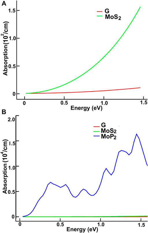
FIGURE 8. We present the absorption in the infrared region. Results for MoS2 and graphene: (A); for graphene, MoS2 and MoP2: (B).
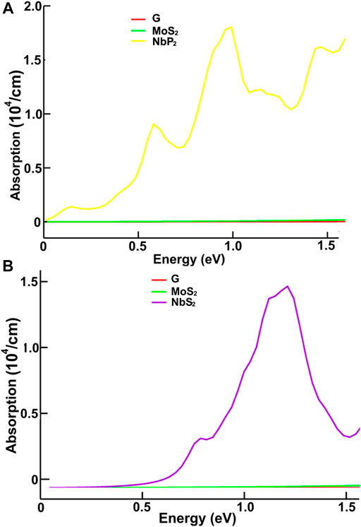
FIGURE 9. We present the absorption in the infrared region. Results for MoS2, NbP2, and graphene: (A); for graphene, MoS2 and NbS2: (B).
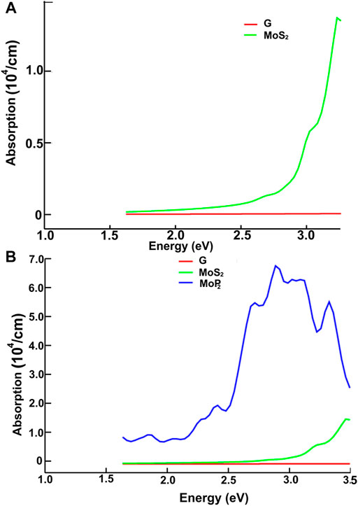
FIGURE 10. We present the absorption in the visible range. Results for MoS2 and graphene: (A); for graphene, MoS2 and MoP2: (B).
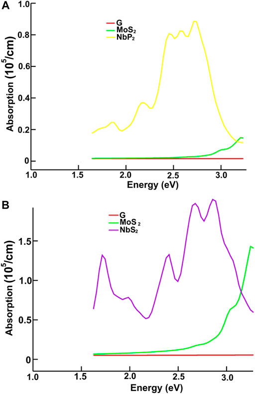
FIGURE 11. We present the absorption in the visible range. Results for graphene, MoS2 and NbP2: (A); for graphene, MoS2 and NbS2: (B).
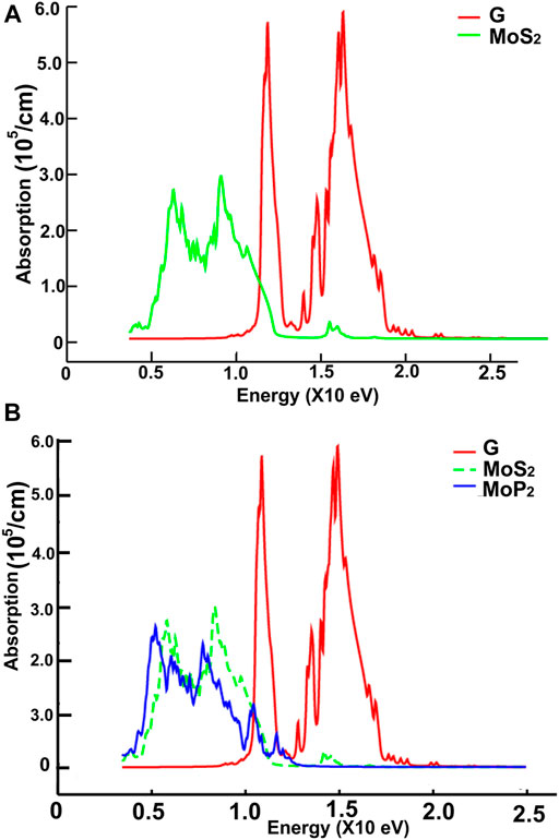
FIGURE 12. We present the absorption in the ultraviolet region. Results for MoS2 and graphene: (A); for graphene, MoS2 and MoP2: (B).
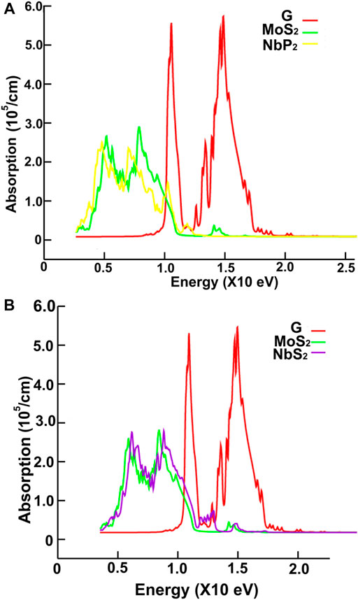
FIGURE 13. We present the absorption in the ultraviolet range. Results for graphene, MoS2 and NbP2: (A); for graphene, MoS2 and NbS2: (B).
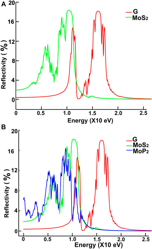
FIGURE 14. We present our calculations for the reflectivity. Results for MoS2 and graphene: (A); for graphene, MoS2 and MoP2: (B).
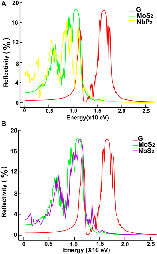
FIGURE 15. We present our results for reflectivity. Results for graphene, MoS2 and NbP2: (A); for graphene, MoS2 and NbS2: (B).
Absorption
We present our results in Figures 8–11. Figures 8, 9 show our results for the infrared region. We compare graphene’s absorption. We found absorptions of ultrathin 2D materials far more significant than that of graphene, from infrared to the spectrum’s visible ranges.
In the infrared, the optical absorption of graphene is near zero. The corresponding MoS2 is around one thousand times larger. The optical absorptions of MoP2, NbS2, and NP2 are about one million times larger than graphene. It is straightforward to understand these results from the energy band structure. The density of bands below the Fermi energy in graphene is much smaller than in the other materials. Thus, the energy required to pass from one allowed state to another above the Fermi energy may be smaller in the other four materials.
Furthermore, This density is more significant in MoP2, NbS2, and NbP2 than in MoS2; Besides, MoS2 presents a bandgap of 1.7 eV. In this manner, more allowed transitions for the electrons, using low energy in MoP2, NbS2, and NbP2 (which are metallic) than in MoS2; and more low energy transitions in MoS2 than in graphene. The absorption peak for MoP2 in Figure 8B at about 1.5 eV comes from the excitations shown with arrows labeled “inf” in Figure 6B. In the same way, we used the same label in Figures 7C,D to indicate transitions related to the absorption peaks for NbS2 at 1.25 eV and NbP2 at 1.0 eV.
Figures 10, 11 present our results for the visible range. Note that the values for graphene remain near zero. The values for MoS2 increase quickly. The absorption value of MoP2 augments, reaching a peak around 2.7 eV, begins to diminish; at around 3.3 eV, its value is close to the value for MoS2. The top for NbS2 is at 1.2 eV and NbP2 at 0.95 eV; the magnitudes for MoP2, NbS2, and NbP2 are similar. From the energy band structure features, it is easy to understand the differences in the absorption spectra. Notice that there are few bands, within this energy range (around 1.6–3.5 eV), in the band structure of graphene to allow these transitions. Thus, the absorption in graphene is deficient compared with the other four materials. We used the label “vis” in Figures 6B, 7A,B to indicate some transitions related to the absorption peaks of MoP2 at 2.75 eV, of NbP2 at 2.5 eV, and NbS2 at 2.8 eV.
Figures 10, 11 show our calculations for the ultraviolet range. The optical absorption for graphene has only two significant peaks, one is around 11.5 eV, and the other is around 16 eV. The four materials show two maxima, which are about one-half the size of the corresponding peak values of graphene. For the four materials, the peaks around 5 and 8 eV. In this energy range of the incident electromagnetic radiation, the absorption in graphene is more similar to the other four materials. The energy band structures show more possible transitions for this energy range (from around five to about 20 eV). In figures corresponding to the band structure (Figures 6A,B, 7A,B), we use the labels “uv1” and “uv2” to show some transitions associated with the two prominent peaks for the absorption for the four materials; MoS2 (at 5.8 and 8.8 eV); MoP2 (at 5 eV and 8 V); NbS2 (at 6.1 and 9.3 eV), and NbP2 (at 5 and 7.1 eV).
Reflectivity
We show in Figures 12, 13 our calculations for the reflectivity.
The reflectivity for graphene is nearly zero for the infrared and visible parts of the spectrum. It has two prominent peaks, around 11.5 and 16 eV. The four ultra-thin 2D materials have much larger reflectivity than graphene. However, all of them go to zero at around 15 eV. Graphene’s reflectivity has its most significant peak at about 16 eV, and then it goes to zero at approximately 24 eV.
Our results for the absorption and reflectivity for MoS2 agree with calculations from other authors (Pan, 2014). It is the same for NbS2; our work agrees with the results from other authors (Elkana Kipkogei Rugut, 2017). However, as far as we know, there are no other previous reports on calculations of the optical absorption and reflectivity for 2D MoP2 or 2D NbP2.
Conclusion
We performed numerical simulations with density functional theory to optimize the geometry of four ultra-thin 2D materials, MoS2, MoP2, NbS2, and NbP2. We obtained that NbP2 should be a new ultra-thin 2D material. To test the stability of this predicted 2D material, we optimized its structure using FPMD. We calculated the energy band structure and the optical absorption and reflectivity of each of the four ultra-thin materials and graphene for comparison.
We found that the absorptions of the four ultra-thin materials are far more significant than that of graphene, from infrared up to the visible region of the spectrum.
In the ultraviolet range, the absorptions of the four ultra-thin 2D materials are like each other and resemble graphene. The absorptions of all five materials show two peaks. However, the sizes of these peaks are about one-half of those of the corresponding peak values of graphene. The maxima are located between 5 and 8 eV for the four materials and displaced about 0.9 eV to the left compared with the graphene spectrum. The peaks for graphene are at 11.5 and 16 eV.
The reflectivity for graphene is nearly zero for both the infrared and visible parts of the spectrum. However, in the ultraviolet range, it shows two peaks around 12 and 16 eV. In contrast, the other four materials have much larger reflectivity than that of graphene below 11 eV. They all have their most significant values below 12 eV. These values are comparable to the maximum reflectivity of graphene. However, all of them decrease to zero at around 15 eV. Graphene’s reflectivity has its most prominent peak at about 16 eV, and it goes to zero around 24 eV.
Data Availability Statement
The original contributions presented in the study are included in the article/Supplementary Material, further inquiries can be directed to the corresponding author.
Author Contributions
Conceptualization and methodology, LM; validation, formal analysis, investigation, EG, OS, and LM; resources, LM; data curation, EG and OS; writing—original draft preparation, LM; writing—review, EG, OS, and LM; project administration, funding acquisition, LM.
Funding
We thank Direction General de Asuntos del Personal Académico de la Universidad Nacional Autónoma de México, partial financial support by Grant IN-113220.
Conflict of Interest
The authors declare that the research was conducted in the absence of any commercial or financial relationships that could be construed as a potential conflict of interest.
Acknowledgments
We appreciate UNAM-Miztli-Super-Computing Center’s technical assistance with the project LANCAD-UNAM-DGTIC-030.
References
Blöch, P. E., Jepsen, O., and Andersen, O. K. (1994). Improved Tetrahedron Method for Brillouin-Zone Integrations. Phys. Rev. B. 49, 16223. doi:10.1103/PhysRevB.49.16223
Brivio, J., Alexander, D. T. L., and Kis, A. (2011). Ripples and Layers in Ultrathin MoS2 Membranes. Nano Lett. 11, 5148–5153. doi:10.1021/nl2022288
Das, S., Robinson, J. A., Dubey, M., Terrones, H., and Terrones, M. (2015). Beyond Graphene: Progress in Novel Two-Dimensional Materials and van der Waals Solids. Annu. Rev. Mater. Res. 45, 1–27. doi:10.1146/annurev-matsci-070214-021034
Elkana Kipkogei Rugut (2017). Numerical Simulation of Structural, Electronic, and Optical Properties of Transition Metal Chalcogenides. Johannesburg, South Africa: University of the Witwatersrand. MSc. Thesis.
Fasolino, A., Los, J. H., and Katsnelson, M. I. (2007). Intrinsic Ripples in Graphene. Nat. Mater 6, 858–861. doi:10.1038/nmat2011
Frenkel, D., and Smit, B. (2001). Understanding Molecular Simulation. London: Academic Press. From Algorithms to Applications.
Ganatra, R., and Zhang, Q. (2014). Few-Layer MoS2: A Promising Layered Semiconductor. ACS Nano 8, 4074–4099. doi:10.1021/nn405938z
Gao, Y., Zhang, M., Ding, J., Hong, S., Masa, J., Liu, S., et al. (2018). Simple Synthesis of Two-Dimensional MoP2 Nanosheets for Efficient Electrocatalytic Hydrogen Evolution. Electrochemistry Commun. 97, 27–31. doi:10.1016/j.elecom.2018.09.018
Giannozi, P., Baroni, S., Bonini, N., Calandra, M., Car, R., Cavazzoni, C., et al. (2009). QUANTUM ESPRESSO: A Modular and Open-Source Software Project for Quantum Simulations of Materials. J. Phys. Condens. Matter 21, 395502. doi:10.1088/0953-8984/21/39/395502
Gmelin Handbuch Der Anorganischen Chemie (1968). Handbuch der Anorganischen Chemie. eighth edn., Vol. 14B/2. Weinheim: Verlag Chemie, 143.
Hullinger, F. (1964). New Representatives of the NbAs2 and ZrAs2 Structures. Nature 204, 775. doi:10.1038/204775a0
Joensen, P., Frindt, R. F., and Morrison, S. R. (1986). Single-layer MoS2. Mater. Res. Bull. 21, 457–461. doi:10.1016/0025-5408(86)90011-5
Kačmarčík, J., Pribulová, Z., Marcenat, C., Klein, T., Rodière, P., Cario, L., et al. (2010). Specific Heat Measurements of a Superconducting NbS2 Single crystal in an External Magnetic Field: Energy gap Structure. Phys. Rev. B. 82, 014518. doi:10.1103/PhysRevB.82.014518
Kokalj, A. (1999). XCrySDen-a New Program for Displaying Crystalline Structures and Electron Densities. J. Mol. Graphics Model. 17, 176–179. doi:10.1016/S1093-3263(99)00028-5
Kumar, S., Maurya, T. K., and Auluck, S. (2008). Electronic and Optical Properties of Ordered BexZn1−xSe Alloys by the FPLAPW Method. J. Phys. Condens. Matter 20, 075205. doi:10.1088/0953-8984/20/7/075205
Maldonado, M., da Silva Neto, M. L., Vianna, P. G., Ribeiro, H. B., Gordo, V. O., Carvalho, I. C. S., et al. Femtosecond Nonlinear Optical Properties of 2D Metallic NbS2 in the Near Infrared. J. Phys. Chem. C. (2020). 124, 15425–15433. doi:10.1021/acs.jpcc.0c02383
Marx, D., and Hutter, J. (2009). Ab Initio Molecular Dynamics, Basic Theory and Advanced Methods. Cambridge: Cambridge University Press. doi:10.1017/cbo9780511609633
Marx, H. (2000). “Ab Initio molecular Dynamics: Theory and Implementation,” in Modern Methods and Algorithms of Quantum Chemistry. Editor J. Grotendorst (Jülich, Germany: NIC, FZ Jülich), 301–449.
Mermin, N. D. (1968). Crystalline Order in Two Dimensions. Phys. Rev. 176, 250–254. doi:10.1103/PhysRev.176.250
Meyer, J. C., Geim, A. K., Katsnelson, M. I., Novoselov, K. S., Booth, T. J., and Roth, S. (2007). The Structure of Suspended Graphene Sheets. Nature 446, 60–63. doi:10.1038/nature05545
Miró, P., Audiffred, M., and Heine, T. (2014). An Atlas of Two-Dimensional Materials. Chem. Soc. Rev. 43, 6537–6554. doi:10.1039/c4cs00102h
Miró, P., Ghorbani-Asl, M., and Heine, T. (2013). Spontaneous Ripple Formation in MoS2 Monolayers: Electronic Structure and Transport Effects. Adv. Mater. 25, 5473–5475. doi:10.1002/adma.201301492
Monkhorst, H. J., and Pack, J. D. (1976). Special Points for Brillouin-Zone Integrations. Phys. Rev. B 13, 5188–5192. doi:10.1103/PhysRevB.13.5188
Morosin, B. (1974). Structure Refinement on NbS2. Acta Crystallogr. Sect B 30, 551–552. doi:10.1107/S0567740874003220
Novoselov, K. S., Geim, A. K., Morozov, S. V., Jiang, D., Katsnelson, M. I., Grigorieva, I. V., et al. (2005). Two-dimensional Gas of Massless Dirac Fermions in Graphene. Nature 438, 197–200. doi:10.1038/nature04233
Novoselov, K. S., Geim, A. K., Morozov, S. V., Jiang, D., Zhang, Y., Dubonos, S. V., et al. (2004). Electric Field Effect in Atomically Thin Carbon Films. Science 306, 666–669. doi:10.1126/science.1102896
Pan, H. (2014). “Progress on the Theoretical Study of Two-Dimensional MoS2 Monolayer and Nanoribbon,” in MoS2. Lecture Notes in Nanoscale Science and Technology. Editor Z. Wang (Springer), 21, 1–35. doi:10.1007/978-3-319-02850-7_1
Payne, M. C., Teter, M. P., Allan, D. C., Arias, T. A., and Joannopoulos, J. D. (1992). Iterative Minimization Techniques Forab Initiototal-Energy Calculations: Molecular Dynamics and Conjugate Gradients. Rev. Mod. Phys. 64, 1045–1097. doi:10.1103/revmodphys.64.1045
Perdew, J. P., Burke, K., and Ernzerhof, M. (1996). Generalized Gradient Approximation Made Simple. Phys. Rev. Lett. 77, 3865–3868. doi:10.1103/PhysRevLett.77.3865
Rani, P., Dubey, G. S., and Jindal, V. K. (2014). DFT Study of Optical Properties of Pure and Doped Graphene. Physica E: Low-dimensional Syst. Nanostructures 62, 28–35. doi:10.1016/j.physe.2014.04.010
Schaak, R. E. (2014). Amorphous Molybdenum Phosphide Nanoparticles for Electrocatalytic Hydrogen Evolution. Chem. Mater. 26, 4826–4831. doi:10.1021/cm502035s
Soto, V., Knorr, K., Ehm, L., Baehtz, C., Winkler, B., and Avalos-Borja, M. (2004). High-pressure and High-Temperature Powder Diffraction on Molybdenum Diphosphide, MoP2. Mop2. Z. Kristallogr. 219, 309–313. doi:10.1524/zkri.219.6.309.34642
Troullier, N., and Martins, J. L. (1991). Efficient Pseudopotentials for Plane-Wave Calculations. Phys. Rev. B 43, 1993–2006. doi:10.1103/PhysRevB.43.1993
Keywords: ultra-thin materials, 2D materials beyond graphene, energy band structure, optical properties, diphosphides, disulfides
Citation: Garcés E, Salas O and Magaña LF (2021) Optical Absorption and Reflectivity of Four 2D Materials: MoS2, MoP2, NbS2, and NbP2. Front. Mater. 8:720768. doi: 10.3389/fmats.2021.720768
Received: 04 June 2021; Accepted: 07 July 2021;
Published: 20 July 2021.
Edited by:
Weiliang Wang, Sun Yat-Sen University, ChinaReviewed by:
Debnarayan Jana, University of Calcutta, IndiaRaad Edaan Haleoot, Al-Mustansiriya University, Iraq
Copyright © 2021 Garcés, Salas and Magaña. This is an open-access article distributed under the terms of the Creative Commons Attribution License (CC BY). The use, distribution or reproduction in other forums is permitted, provided the original author(s) and the copyright owner(s) are credited and that the original publication in this journal is cited, in accordance with accepted academic practice. No use, distribution or reproduction is permitted which does not comply with these terms.
*Correspondence: L. F. Magaña, fernando@fisica.unam.mx