
Abstract
The light extraction efficiency (LEE), external quantum efficiency (EQE), and current–voltage characteristics of deep ultraviolet light emitting diodes (DUV-LEDs) with different aluminum mole fractions in the p-AlGaN layers have been investigated. Optimizing the p-AlGaN layer composition requires a tradeoff between reducing the absorption losses and limiting the increases in the p-contact resistance and operation voltage. AlGaN multiple quantum well LEDs emitting around 263 nm with different AlGaN:Mg short period super lattices (p-SPSL) ranging from x = 33% (UV-absorbing) to x = 68% (UV-transparent) average aluminum mole fraction have been explored. DUV-LEDs with different p-contact metals and UV-reflectivities have been characterized by electroluminescence measurements and analyzed by ray-tracing simulations. The comparison shows an increased operating voltage and a five-fold increase of the on-wafer EQE with a maximum value of 3.0% for DUV-LEDs with UV-transparent p-SPSL (x = 68%) and UV-reflective indium contacts in comparison to LEDs with a UV-absorbing p-SPSL (x = 33%). Ray-tracing simulations show that the increase in EQE can be partially ascribed to a 2.5-fold improved LEE in combination with a two-fold increase in internal quantum efficiency.
Export citation and abstract BibTeX RIS

Original content from this work may be used under the terms of the Creative Commons Attribution 4.0 license. Any further distribution of this work must maintain attribution to the author(s) and the title of the work, journal citation and DOI.
1. Introduction
Typically the p-side of deep ultraviolet light emitting diodes (DUV-LEDs) utilizes highly absorbing p-GaN contact layers and a low aluminum mole fraction p-(Al)GaN heterostructure [1–4]. Such approach enables low series resistances in the p-layers as well as ohmic p-contacts resulting in low operating voltages that can be close to the diode built-in potential. However, the strong UV-absorption in the p-(Al)GaN layers limits the external quantum efficiency (EQE) of such devices due to the resulting poor light extraction efficiency (LEE). To realize high power LEDs with a high EQE, a UVC-transparent p-AlGaN heterostructure in combination with highly UV-reflective p-metal contacts is required to enhance the light extraction [4–10]. However, it has been experimentally observed that high aluminum mole fraction p-AlGaN layers show higher series resistances, higher contact resistances as well as higher operating voltages thus reducing the wall plug efficiency [11, 12].
In this paper, the effects of the AlGaN:Mg/AlGaN:Mg short period super lattice (SPSL) of AlGaN-based DUV-LEDs and the p-contact metal on the electro-optical characteristics and LEE are investigated by electroluminescence (EL) measurements and Monte-Carlo ray-tracing simulations. In particular, LEDs with highly UV-absorbing and UV-transparent p-AlGaN SPSL as well as UV-absorbing and UV-reflective p-contacts were compared with regards to their operation voltages, EQE, LEE, and internal quantum efficiency (IQE). Here, the IQE is the product of the radiative recombination efficiency and charge carrier injection efficiency and was determined from the ratio between the measured EQE and simulated LEE [1]. For this study a series of DUV-LEDs with UV-transparent and UV-absorbing p-side (different Al mole fractions in the p-AlGaN SPSL) as well as three different p-contact metal stacks with high and low UV-reflectivity have been investigated.
2. Experimental
The DUV-LEDs were grown by metal organic vapor phase epitaxy on (0001) oriented epitaxially laterally overgrown (ELO) AlN/sapphire templates with threading dislocation densities of 1.4 × 109 cm−2 [13]. The hetero-structure consists of a 1 µm thick Al0.76Ga0.24N:Si current spreading layer, a 200 nm thick Al0.65Ga0.35N:Si contact layer [14], a three-fold multiple quantum well (MQW) active region with 1.4 nm thin Al0.48Ga0.52N quantum wells and 5 nm thick Al0.63Ga0.37N barriers, a 10 nm Al0.85Ga0.15N interlayer, a 25 nm Al0.75Ga0.25N:Mg electron blocking layer and a 90 nm thick Alx Ga1−x N:Mg/Aly Ga1−y N:Mg SPSL with a layer thickness of 3 nm/3 nm (figure 1). Four different DUV-LED heterostrucutres were grown with nominal Al mole fractions x/y in each SPSL layer of 0.29/0.37, 0.41/0.48, 0.55/0.62, and 0.65/0.71. However, an optically relevant average Al mole fraction in the p-AlGaN SPSL of 33%, 44%, 58% and 68%, respectivly, was determined by high resolution x-ray diffraction reciprocal space maps (RSM). The RSMs indicate a pseudomorphic growth of the whole heterostructure for all p-AlGaN SPSL compositions.
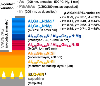
Figure 1. Schematic sketch of the DUV-LED heterostructure, the variation in the p-AlGaN SPSL with nominal well Al mole fraction x, nominal barrier Al mole fraction y and measured average Al mole fraction Ø, as well as the variation of the p-contact metallization.
Download figure:
Standard image High-resolution imageAll wafers were processed with standard micro-fabrication techniques into LEDs with an active area of 0.02 mm2. The LEDs feature V/Al-based annealed n-contacts [15] and three different types of p-contacts for comparision (figure 1): a 200 nm thick Au contact, a Pd/Al/Au (2 nm/200 nm/200 nm) metal stack, and a 200 nm thick indium contact, hereafter referred as Au, Pd+Al, and In, respectively. Only the Au contact was thermally annealed at 500 °C for 1 min in N2, while the Pd+Al and In contacts were tested as deposited. As these metals are in direct contact with the p-AlGaN SPSL, there was no intent in optimizing the p-contact resistance. Therefore, a comparison of the wall plug efficiency between these LEDs was not considered. The optical and electrical characterization has been performed by on-wafer EL measurements with a calibrated UV-enhanced Si photodiode and a fiber spectrometer under continuous wave operation at room temperature without active cooling. For transmission and reflection measurements, a Shimadzu UV-2600 UV–VIS spectrophotometer was used in a free beam configuration orthogonal to the surface. The LED transmission spectra were measured on the full LED structure before processing and the metal reflectivities were measured through double side polished sapphire samples.
The simulation of the LEE is based on Monte-Carlo ray-tracing simulations taking into account the dispersion of refractive indices [16], the reflectivity of the different metal contacts and an in-plane degree of polarization (ITE − ITM)/(ITE + ITM) of 0.92 for the light polarization and emission pattern of the active region [17]. The absorption within the AlGaN MQW and the n-AlGaN heterostructure layers were assumed to be 103 cm−1 and 10 cm−1, respectively [18, 19], while the absorption of the p-AlGaN was determined by transmission measurements. The ray-tracing simulations take also into account the finite size of the Si photodiode with a detection area of 1 cm2 positioned 3.0 mm below the wafer as well as the light scattering at the ELO AlN/sapphire interface and the rough sapphire backside [20]. The latter is based on a model which takes into account the surface inclination angle distributions that change the ray path through the interface. Here, the rough sapphire backside (with a root mean square value of 0.7 µm) and the rough ELO inner interfaces have a mean inclination angle of 18° and 63° with a full width at half maximum of 30° and 45°, respectively, both nearly normally distributed [21].
3. Results
3.1. Transmission and reflection measurements
In order to obtain key parameters for the ray-tracing simulations, the reflectivities of the different p-contact metals and the transmission spectra of the different LED heterostructures were measured. Figure 2(a) shows the reflectivities of Au, Pd+Al, and In metal contacts measured on double side polished sapphire substrates as a function of the wavelength. Additional reflections from the sapphire/air interface are subtracted during the evaluation. The spectrum of a fully-transparent LED (also shown in figure 2) exhibits a single emission peak around 263 nm and a full width at half maximum of 10 nm. In the relevant region of the QW emission between 255 nm and 275 nm, the reflectivities of Au, Pd+Al, and In are RAu = 24%, RPd+Al = 63%, and RIn = 87%, respectively. Based on these experimental results, refractive indices of nAu = 1.3 + 1.65 i [22], nPd+Al = 0.6 + 2.4 i [23, 24], and nIn = 0.2 + 2.7 i [25], were used in the ray-tracing simulation for the Au, Pd+Al, and In contacts, respectively. Figure 2(b) shows the transmission spectra of four different LED heterostructures with an average aluminum mole fraction in the p-AlGaN SPSL between x = 33% and x = 68%. The transmission is normalized to the transmission at 263 nm of the LEDs with x = 68%, assuming a negligible absorption of the p-AlGaN SPSL of ⩽102 cm−1 [26]. All transmission spectra show a slight reduction in the transmission with decreasing wavelength which is mainly attributed to losses by light scattering at the ELO AlN/sapphire and sapphire/air interface. Furthermore, all samples show an absorption edge below 250 nm corresponding to the absorption edge of the Al0.65Ga0.35N:Si contact layer. A second absorption tail is visible below 300 nm for x = 33%, 280 nm for x = 44%, and below 265 nm for x = 58% corresponding to the absorption edges of the respective AlGaN:Mg SPSL layers. Using the transmission values at the peak emission wavelength of 263 nm absorption coefficients of 1.5 × 105 cm−1, 1.2 × 105 cm−1, 7 × 103 cm−1 were evaluated by the Beer–Lambert law for the p-AlGaN SPSL with x = 33%, 44%, and 58%, respectively.

Figure 2. In both graphs the typical emission spectrum from a fully-transparent LED at 5 mA is shown in gray in the background. (a) Measured reflectivity of Au, Pd+Al and In on double side polished sapphire as a function of the wavelength. (b) Transmission spectrum of the entire LED heterostructure structure as a function of the emission wavelength for different aluminum mole fractions in the p-AlGaN SPSL normalized to the transmission at 263 nm of the LEDs with 68% Al mole fraction in the p-AlGaN SPSL.
Download figure:
Standard image High-resolution image3.2. Ray-tracing simulations
Based on the experimentally determined absorption coefficients and contact reflectivities, ray-tracing simulations were performed. Figure 3 shows the simulated extracted light intensity of an LED on wafer as a function of the emission angle θ of the AlGaN MQW active region. An angle of θ = 0° refers to an emission in the substrate direction, θ = 180° refers to emssion directed towards the p-contact, and θ = 90° correspond to emission in in-plane direction. Note that the light intensity (unit: one per degree) at a particular angle θ is integrated over the radiant intensity (unit: one per steradian) over all azimuthal angles. The grey line indicates the radiation emitted by the active region whereas the differently hatched areas denote the extracted light for certain heterostructures and templates. Since the integral of the grey line is normalized to 1, this method allows an interpretation of the hatched area under the curve as the LEE. LEDs with UV-absorbing (x = 33%) and UV-transparent (x = 68%) p-AlGaN SPSL―both with In p-contacts―as well as smooth sapphire backside with flat AlN/sapphire interface (labeled as 'smooth') and rough sapphire backside with patterned ELO AlN/sapphire interface (labeled as 'rough & ELO') are shown. The intensity of the active region (figure 3, gray) increases sharply with increasing emission angle and reaches a broad plateau of 6.8 × 10⁻³/° for 40° < θ < 140°. This distribution is a product of the dominant TE polarized radiation pattern and the integration over all azimuthal angles. For smooth interfaces and DUV-LEDs with a UV-absorbing p-AlGaN SPSL, the light extraction is limited to an escape cone of θ = 22° due the refractive index (n) difference between the active region (n = 2.64) and air (n = 1.0). The remaining emission is totally internally reflected and eventually absorbed at the n-contacts and the UV-absorbing p-AlGaN SPSL, resulting in an overall LEE of only 4.5%. For the LED with a UV-transparent p-AlGaN SPSL and smooth interfaces the light extraction is still limited to an escape cone of θ = 22° but also light emitted to θ > 158° can be partly reflected at the In contact and extracted through the substrate leading to a nearly doubled LEE of 8.1%. This intuitive result changes with the introduction of the patterned AlN/sapphire interface and rough sapphire/air interface. For the LED with a UV-absorbing p-AlGaN SPSL, the light extraction is again limited to the bottom hemisphere (θ < 90°) but the light escape cone is now increased to θ = 60°, given by the change of refractive index between n-AlGaN and AlN. Due to the patterned AlN/sapphire interface, the light extraction is reduced for θ < 22° due to light scattering but improved for 22° < θ < 60° due to the partially suppressed total reflection at the AlN/sapphire and sapphire/air interfaces. The LEE is slightly improved from 4.5% ('smooth') to 5.1% ('rough & ELO'). For the LED with a UV-transparent p-AlGaN SPSL also light emitted to the top hemisphere (θ > 120°) is reflected back and scattered at the patterned AlN/sapphire interface. Due to the possibility of multiple ray paths inside the fully transparent heterostructure the extracted light intensity is increased for 22° < θ < 60° as well as for θ > 120° compared to the UV-absorbing p-AlGaN SPSL. In this optimized case the LEE is 13.4% and 2.5 times larger than for the LED with UV-absorbing p-AlGaN SPSL.
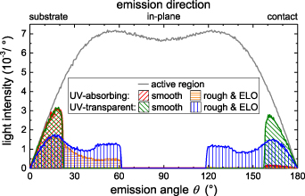
Figure 3. Simulated extracted light intensity (LED on wafer) as a function of the emission angle θ inside the active region integrated over the radiant intensity over all azimuthal angles in case of LEDs with an UV-absorbing p-AlGaN SPSL and smooth interfaces (red, diagonal right up striped), a UV-absorbing p-AlGaN SPSL and rough sapphire backside and ELO AlN/sapphire (orange, horizontal striped) as well as a fully-transparent p-AlGaN SPSL and smooth interfaces (green, diagonal right down striped), and a fully-transparent p-AlGaN SPSL and rough sapphire backside and ELO AlN/sapphire (blue, vertical striped).
Download figure:
Standard image High-resolution image3.3. Electroluminescence measurements
Figure 4 shows the typical current–voltage-characteristics as well as the on-wafer emission powers as a function of the current for LED with x = 33% average Al mole fraction in the p-AlGaN SPSL (UV-absorbing) and a fully-transparent LED with x = 68% in case of Au, Pd+Al and In p-contacts. Note that, due to the high contact resistance of p-contacts on high Al mole fraction AlGaN:Mg layers the maximum current for the Pd+Al p-contacts was 15 mA for x = 33% and only 6 mA for x = 68%. For the UV-absorbing p-AlGaN SPSL (figure 4(a)), the turn-on voltage for the LEDs at a current density of 1 A cm−2 is between 5.6 V and 6.3 V. Transfer-length method measurements exhibit an ohmic behavior for the n-contact but a rectifying behavior for the p-contacts. Therefore the higher voltage of the LED in comparison to the built-in potential of 4.7 V is most likely attributed to the large Schottky barrier height of the p-AlGaN/metal interface. Nevertheless, the LED with a Au p-contact has the lowest turn-on voltage for the different p-contacts, which we attribute to the larger work function of 5.1 eV for Au compared to 4.1 eV for In [27]. The on-wafer measured emission power increases nearly linearly with increasing injection current and reaches 0.5 mW at 20 mA independent of the p-contact metal. Due to the strong UV-absorption in the p-AlGaN SPSL the LEE is independent of the metal reflectivity. For the fully-transparent LED (figure 4(b)), the turn-on voltage of the device is larger than 10 V. This can be most likely attributed to the higher aluminum mole fraction in the p-SPSL resulting in a more pronounced Schottky barrier at the p-AlGaN/metal interface and an increasing resistivity of the p-AlGaN SPSL layer [11, 12]. The on-wafer measured emission power increases again nearly linearly with increasing injection current but shows the beginning of a thermal rollover for currents exceeding 5 mA due to Joule heating. However, the emission power of 2.1 mW at 20 mA in case of In p-contact (RIn = 87%) is higher than 1.2 mW at 20 mA in case of Au p-contact (RAu = 24%), while the emission power of the LED with Pd+Al p-contact (RPd+Al = 63%) is in-between those with an In or Au p-contact. Due to reduced absorption in the UV-transparent p-AlGaN SPSL, the light extraction is strongly affected by the metal reflectivity of the p-contacts. Furthermore, all reached emission powers of LEDs with UV-transparent p-AlGaN SPSL are also much higher in comparison to the emission power of LEDs with UV-absorbing p-AlGaN SPSL (i.e. 0.5 mW). Due to the low absorption in the UV-transparent p-AlGaN SPSL, multiple reflections between a highly reflective p-contact and the patterned AlN/sapphire are possible. The light scattering at the patterned AlN/sapphire then increases the probability for the light to escape.
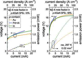
Figure 4. Typical voltage vs current (solid line) and on-wafer emission power vs current characteristics (dashed line) for DUV-LEDs with (a) 33% (UV-absorbing) and (b) 68% (UV-transparent) aluminum mole fraction in the p-AlGaN SPSL in case of Au, Pd+Al or In p-contacts.
Download figure:
Standard image High-resolution imageTo compare the results of the entire series at least five LEDs for each p-AlGaN SPSL and for each p-contact type were measured and the EQE was evaluated at 5 mA (corresponding to a current density of 25 A cm−2) before thermal rollover. Figure 5 shows the measured EQE (on-wafer), the simulated LEE, as well as the calculated IQE by the quotient of EQE and LEE as a function of the avg. aluminum mole fraction of the p-AlGaN SPSL. It should be mentioned that the simulated LEE considers the pure detectable light emission on the experimental setup. For the UV-absorbing p-AlGaN SPSL (x = 33% and x = 44%, figure 5(a)), the EQE is less than 0.8% and nearly independent of the p-contact metal. In contrast, the EQE is higher than 1.2% for the UV-transparent p-AlGaN SPSL (x = 58% and x = 68%), clearly affected by the p-contact reflectivity and up to 3% in case of In contacts. The experiment shows more than a five-fold increase of the EQE between a UV-absorbing and UV-transparent p-AlGaN SPSL with highly reflective In p-contacts. Similarly, the LEE (figure 5(b)) is nearly constant at 4% for x = 33% and x = 44% and independent from the p-contact metal. For x = 58% and x = 68%, the LEE increases and differentiates depending on the p-contact reaching a maximum of 10% for x = 68% and In p-contacts, matching the predicted improvement of a factor of 2.5.

Figure 5. (a) On-wafer measured external quantum efficiency (EQE) at 5 mA direct current, (b) simulated setup light extraction efficiency (LEE), and (c) calculated internal quantum efficiency (IQE) as quotient of EQE and LEE as a function of the average Al mole fraction in the p-AlGaN SPSL in cases of Au, Pd+Al and In p-contacts.
Download figure:
Standard image High-resolution image
4. Discussion
The gain in the measured EQE and the rise in the simulated LEE (figure 5) with increasing average aluminum mole fraction of the p-AlGaN SPSL shows a good qualitative agreement. However, the observed increase in EQE is significantly larger than the simulated increase in LEE with increasing average Al mole fraction in the p-AlGaN SPSL. Therefore additional factors need to be considered. The EQE is defined as the product of IQE and LEE [1]. By dividing EQE with LEE, the resulting IQE (figure 5(c)) shows an increase from 15% at x = 33% to 29% at x = 68% independent from the p-contact type. One explanation may be an underestimation of the simulated LEE for the transparent p-AlGaN SPSL. However, the comparison of three different metals (with different UV-reflectivities) shows a perfect overlap for the IQE values for every p-AlGaN SPSL composition, except for In p-contacts on 44%, which had a processing issue. This indicates a correctly simulated light propagation and scattering, especially in case of the fully-transparent heterostructure. Furthermore, the impact of the Purcel effect seems negligible [28], since the IQE is the same for In (high reflectivity) and Au (low reflectivity) p-contacts. On the other hand, a change in the refractive index near the active region from a UV-transparent p-AlGaN SPSL (n = 2.5 + 0.0 i) to UV-absorbing p-AlGaN SPSL (n = 2.6 + 0.3 i) could change the dipole radiation pattern in the active region [29]. This would lead to an asymmetric radiation profile to the top and bottom hemisphere and thus reduce the LEE. In order to take this effect into account wave optics simulations will be employed but are beyond the scope of this paper. Another explanation could be an improved charge carrier injection efficiency into the AlGaN MQW active region. An increasing aluminum content in the p-AlGaN SPSL reduces the potential barrier between the electron blocking layer and the p-AlGaN SPSL for holes, which could then increase the hole injection. Furthermore, the UV-transparent p-AlGaN SPSL have a higher aluminum mole fraction in the SPSL barriers than in the MQW barriers, which might increases the electron blocking behavior of these devices. At this point, it is not clear whether one of these mechanisms dominates or if all contribute to the observed behavior. Nevertheless, the results show that the optimum Al mole fraction in the p-AlGaN layers are governed by the UV-transparency in order to enhance the LEE as well as the charge carrier confinement in order to maximize the current injection efficiency. In addition the operating voltage increases with higher Al mole fraction due to larger p-AlGaN series resistance and p-contact resistance. Therefore it is not straightforward to find an ideal composition range that satisfies all parameters.
5. Conclusion
In conclusion, the influence of the average Al mole fraction in the AlGaN:Mg/AlGaN:Mg SPSL and the p-contact metal reflectivity on the EQE, LEE and IQE of DUV-LEDs was investigated by EL measurements and ray-tracing simulations. The measured on-wafer EQE shows a five-fold increase of the on-wafer EQE from 0.6% for UV-absorbing p-AlGaN SPSL (x = 33%) to 3.0% for UV-transparent p-AlGaN SPSL (x = 68%) with reflective In p-contacts. This improvement was partially ascribed to a 2.5-fold improved LEE, determined by ray-tracing simulation, in combination with a two-fold increase of the IQE for the UV-transparent p-AlGaN SPSL. The increased IQE could be explained by an improved charge carrier injection due to a reduced potential barrier for holes and enhanced electron blocking effect.
Acknowledgments
The authors would like to thank Sylvia Hagedorn (Ferdinand-Braun-Institut, Leibniz-Institut für Höchstfrequenztechnik, Berlin, Germany) for providing the ELO AlN/sapphire templates for the LEDs. This work was partially supported by the German Federal Ministry of Education and Research (BMBF) within the 'Advanced UV for life' project and by the Deutsche Forschungsgemeinschaft (DFG) within the Collaborative Research Centre 'Semiconductor Nanophotonics' (SFB 787).
Data availability statement
The data that support the findings of this study are available upon reasonable request from the authors.