
Abstract
Pulsed hydrocarbon ions produced in a plasma focus device were used to irradiate different substrate materials (Si, Ti, Mo and W) and to deposit thin films of carbon material over it. High energetic and high intensity pulsed hydrocarbon ions were produced when plasma focus device was filled with 0.5 mbar of acetylene gas and operated at 2 kJ. Effects of substrate materials properties, its thermal evolution under pulsed irradiation of energetic ions and plasma streams on the deposited films have been studied. Visible Raman spectroscopic measurements confirmed that deposited films were of diamond-like-carbon. Fraction of sp3 bonded carbon in films on different substrate materials (16%, 8.7%, 13% and 18.9% on Si, Ti, Mo and W respectively) was found to be correlated to substrate materials thermal properties i.e. high fraction of sp3 bonded carbon was observed over substrate materials having high thermal conductivity. Carbon atom concentrations were measured to be different (22.46 at. %, 22.7 at. %, 10.4 at. % and 32 at. % on Si, Ti, Mo and W respectively) over different substrates. Surface morphologies of DLC were also observed to be different for different substrates. On inserting graphite at anode tip, fraction of sp3 bonded carbon in DLC coating over Si substrate increased to 19.5%.
Export citation and abstract BibTeX RIS
1. Introduction
Diamond-Like-Carbon (DLC) [1], owing to its outstanding properties including high hardness, high thermal conductivity, electrical insulation, low friction coefficient, and chemical inertness, has found many industrial applications [2], These properties of DLC are found to be strongly dependent on its method of formation [3] which has generated vast interest among the researchers across the world. Various methods are currently in use for deposition of DLC thin films at low temperature on various substrate materials of different shapes and sizes. The most popular methods amongst them are plasma enhanced chemical vapor deposition (PECVD) techniques [4–6], vacuum arc deposition [7, 8], pulsed laser deposition (PLD) [9], and ion beam-assisted deposition (IBAD) techniques [10], Nevertheless, the above listed methods required various external agents, e.g. external substrate heating, external DC/RF biasing to substrates, and electric and magnetic fields to focus the electrons/ion beams, either alone or in combination to get high purity and uniform thin films of desired thickness. Plasma focus (PF) devices have also been used for deposition of DLC thin films on various substrates at high deposition rate. Deposition of uniform thin films at room temperature without external heating and/or biasing of substrate makes plasma focus device suitable for depositing thin films of various materials on different substrate materials, suitable to many applications. Moreover, their simple design and operation at a relatively low cost has also proven to be beneficial for such applications.
Plasma focus device [11] is a well-known pulsed source of hot plasma streams, ions, electrons, X-rays and neutrons (with deuterium or deuterium-tritium mixture gas only). Depending on applications, it is operated with different filling gases e.g. Hydrogen (H2), Deuterium (D2), Neon (Ne), Nitrogen (N2), Methane (CH4) and Argon(Ar) for producing energetic ions and plasma streams of respective gases and its constituents. The ions are of wide energies ranging from a few keV to several hundreds keV and plasma stream has high speed of ≥105 m s−1 [12–15]. These ion and plasma streams have been used for many applications like for irradiation on various fusion reactor relevant materials [16–19] and for deposition of thin films of various materials on different substrate materials. For example, Rawat [20] and Ghareshabani et al [21] have used a low energy (219 J) plasma focus device filled with hydrogen gas for deposition of DLC on Si(100) substrate. Bhuyan et al [22] reported formation of surface layer of hexagonal silicon carbide on Si(100) substrate using a low energy (2.2 kJ) plasma focus device operated with methane gas. Production of different types of sub-micron characteristic size carbon composite coatings using high energy carbon ion beam irradiation of solid targets such as silicon, titanium has also been reported by Bhuyan et al [23]. Soh et al [24] used 3.3 kJ PF device with neon as the filling gas to deposit DLC thin films by ablating the high purity graphite fitted to the top of the anode. Deposition of DLC films on silicon substrates by ablation of graphite anode material with the help of pulsed electron beam in a 1.45 kJ DPF device under nitrogen environment has been reported by S. Zeb et al [25]. Thin films of several other materials such as titanium carbide [26], cobalt platinum (CoPt) [27], iron cobalt (FeCo) [28], zinc-oxide [29], lead zirconate titanate [30] have also been deposited using plasma focus device with selecting the appropriate filling gas, anode and substrate material.
The substrate material is among the various other factors which effect the DLC characteristics as various report suggests. Moreover, thermal evolution of substrate surface temperature under irradiation of pulsed energetic and intense ions is also expected to influence the DLC characteristics. In view of this, deposition of DLC thin films over substrates of different materials namely Silicon (Si), Titanium (Ti), Molybdenum (Mo) and Tungsten (W) using a low energy operating plasma focus device has been presented. Moreover, the plasma focus device has been used as a simple and economical tool to understand the effects of substrate material properties on the DLC films characteristics and vice versa, as the DLC coating is also applied over various materials to improve their surface properties suitable for various industrial applications [2] as also mentioned above. Different substrate materials with widely different physical and thermal properties have been chosen to understand their effects on the various characteristics of the deposited DLC thin films such as chemical bond characteristics, surface morphologies, carbon atom concentrations, thickness among others. In addition, effects of graphite ablation on the characteristics of the DLC thin films have also been studied by inserting graphite material at its anode tip. A comprehensive analysis of the effects of different substrate materials as well as of ablation of the graphite material on the properties of DLC thin films has been presented here.
2. Experimental methods
The plasma focus device used in present study has been assembled in house. A schematic of the experimental set up has been shown as figure 1(a).The plasma focus electrodes geometry was of Mather type and of squirrel cage geometry. The cathode, consisting of twelve rods (each 10 mm diameter), was placed around the anode at 90 mm pitch circle diameter (PCD). The anode was in the form of a rod of 30 mm diameter. The length of the anode and the cathode were chosen to be 105 mm and 95 mm respectively. Both electrodes were made out of stainless steel (SS304) material. The tip of the anode was made deep hollow (20 mm diameter × 40 mm deep) to avoid its erosion due to collision of high energetic relativistic electrons post plasma focus disruption. The bottom of the electrodes was closed on a quartz insulator whereas the top was kept open. The external and internal diameter of quartz insulator was 25 mm and 22 mm respectively. The plasma focus electrode assembly was placed inside a high vacuum compatible experimental chamber of volume 4.5 liter. The experimental chamber has two side ports, one of the port was used for its evacuation and filling of the working gas using multiport whereas other port was meant for diagnostics purpose. This complete unit was termed as 'plasma focus load'. A single energy storage capacitor (10 μF, <30 nH, 30 kV) was used as the energy driver for the plasma focus device. A triggered spark gap switch was embedded in between the capacitor and the plasma focus load in a compact assembly as depicted in figure 1(a).

Figure 1. Schematic of the experimental setup (a) with bare hollow anode and (b) graphite inserted anode.
Download figure:
Standard image High-resolution imageIn plasma focus device, plasma is produced through pulsed fast (typically a few μs) electrical discharge of energy stored in the capacitor into a low pressure gas (typically a few mbar). The plasma is accelerated in the annular gap between electrodes and then compressed over the anode tip by the J × B force due to interaction of high discharge current with its self-produced magnetic field. This results into formation of high dense (∼1019 per cm3) and high temperature (≥1 keV) plasma column, termed as 'plasma focus', for a few tens of nanosecond. However, rapid growth of instability (Sausage, m = 0) breaks the plasma focus column, resulting into bursts of high energetic plasma streams and radiations including ions, electrons, X-rays, and neutrons (when the filling gas is D or D-T mixture) for a few tens to one hundred ns. High energetic plasma streams, ions and electrons have been utilized for deposition of thin films of various materials over different substrate materials, since long. Generally, the materials, of which thin film is to be deposited, are fitted at the tip of the anode and the substrate is kept axially away from it. Relativistic electrons moving along axially downward direction [31] [shown in Figure 1(a)] towards the positive PF anode and ablate the anode tip material. The ablated material forms plasma plume near the anode tip and it moves towards the substrate along the anode axis. In order to avoid formation of any composites of evaporated material and operating gas, non-reactive gas such as neon, argon is used as the filling gas in many experiments [24, 29, 30]. In some report, target material was kept along axis which gets sputtered on irradiation of energetic ions. The sputtered atoms get deposited over substrate kept at off axis position. Wang et al [32] has reported the deposition of diamond-like carbon (DLC) films on Si substrates through the ablation of graphite by intense pulsed ion beam emitted from a 20 kJ DPF operated with hydrogen gas. The substrates were mounted on a holder away from the anode tip, which allowed for deposition at positions between normal and 20◦ off-normal to the target.
Here, for deposition of DLC thin films, acetylene (C2H2) gas was used as the filling gas with the bare hollow anode [figure (1(a))] as well as with the graphite inserted to the anode tip [figure 1(b)]. High energetic (a few keV up to MeV) precursor ions of various kinds (C2H+, H+, C+n etc) have been reported to have formed post plasma focus disruption when hydrocarbon gases (CH4, C2H2 etc) were used as filling gas. Typical fluence of precursor ions were observed to be of 1017–1018 ions m−2 with its energies ranging from a few keV to several hundreds of keV [13, 23, 33]. For example, Bhuyan et al [23] have reported the production of ion beam of hydrogen (H+) and carbon of characteristics charge states (C+5 and C+4) of energies ranging between 50 keV and 600 keV using 1.8 kJ, 160 kA plasma focus (PF) device operating in CH4 gas, with a hollow anode. With bare hollow anode, precursor ions move axially away from anode tip and get deposited over substrate kept axially away from it. Whereas with graphite inserted tip, ablated graphite material along with precursor ions also get deposited on the substrate. The distance between the substrate and the anode tip was optimized in order to avoid fracture of the Si substrate due to shock generated in the post plasma focus disruption [12] and also to ensure that precursor ions overcome the collision with background or thermal plasma and reach the substrate with sufficient energy.
The substrates were kept at 10 cm away from anode tip along the axis. At a distance lower than this, the Si substrate was found to be broken in few plasma focus shots due to thermal shock induced by the energetic precursor ions as well as shock generated post plasma focus disruption as earlier mentioned. The Si substrate was cut out in square form of size 8 mm × 8 mm from a large size Si wafer of 0.5 mm thickness whereas other substrates (Ti, Mo and W) were cut into discs of 2 mm thickness from a 10 mm diameter rod of respective materials. They were mirror polished and ultrasonically ringed in alcohol and deionized water for 10 min each before placing in the experimental chamber. The surface roughness (measured using surface profilometer) of the substrate surface along with other properties have been tabulated below (table 1). The substrates were kept at room temperature in the experimental chamber. A shutter, made out of aluminum was placed before substrate to prevent it from exposure to thermal plasma during optimization of plasma focus operation conditions.
Table 1. Various properties of different substrate materials.
| Substrates | Specific heat (J g−1.K−1) | Thermal conductivity [W/(m·K)] | Melting temperature (deg K) | Substrate roughness (nm) |
|---|---|---|---|---|
| Si | 0.71 | 150 | 1687 | 118 |
| Ti | 0.52 | 22 | 1941 | 120 |
| Mo | 0.25 | 139 | 2896 | 211 |
| W | 0.13 | 170 | 3695 | 207 |
Optimum filling pressure of acetylene gas was obtained for operation at 2 kJ. It was essential in order to ensure efficient energy transfer to the plasma at the time of plasma focus formation. This would be translated into high energy and high fluence of precursor carbon ions which would further be useful in depositing uniform thin films at high deposition rate. To obtain optimum filling pressure, it was varied from 0.5 to 3.0 mbar in steps of 0.5 mbar. The experimental chamber was evacuated to a base pressure of ≤10–5 mbar using rotary-diffstak vacuum pumping system before filling with C2H2 gas to the desired pressure. At each filling pressure, plasma focus formation has been observed though the measurement of the discharge current-derivative using in house made Rogowski coil. A plastic scintillator detector in combination with photomultiplier tube was used in the radial direction to measure time-resolved emission of hard x-rays. Typical oscilloscope image of discharge current-derivative and hard x-rays signals for a typical plasma focus discharge have been presented in figure 2. The large dip observed in the current-derivative signal is due to sharp increase in the inductance during fast radial compression of plasma above the anode tip [34]. The form of this dip is signature of plasma focus characteristics. The hard X-rays recorded in the plastic scintillator detector is due to collision of relativistic electrons with plasma focus anode [11] as discussed earlier. Emission of energetic ions in direction opposite to this i.e. away from the anode tip can also be inferred from the hard x-ray emission.

Figure 2. Typical oscilloscope image of current derivative (pink color) and hard x-ray (blue color) signals from plasma focus device.
Download figure:
Standard image High-resolution imageStrong and sharp dip in the current derivative signal was observed at 0.5 mbar filling pressure. This could be the optimum filling pressure for plasma focus operation at 2 kJ capacitor bank energy. Total 200 plasma focus discharges were performed at optimum operation conditions for deposition of the DLC thin films on each substrate (mild or no focus shots have not been included). The mild or no focus was observed in some plasma focus discharges (<3%) mainly due to misfire of the spark gap switch at a voltage lower than the intended operation voltage. After each plasma focus discharge, plasma focus chamber was evacuated to base pressure ≤10–5 mbar using rotary-diffstak vacuum pumping system. Then for next discharge, it was fresh filled with 0.5 mbar of acetylene filling gas. Filling gas pressure before and after discharge was found to be same. The time gap between two plasma focus discharge was kept minimum 5 min. Deposited DLC thin films were characterized using multiple techniques e.g. chemical-bond characteristics using visible Raman spectroscopy, surface morphologies and thickness using scanning electron microscope (SEM), elemental compositions using energy dispersive x-ray spectroscopy (EDS), and roughness of the substrate surface using surface profilometer.
3. Results and discussion
Visible Raman spectroscopic measurements on DLC thin films deposited on different substrates have been carried out using excitation wavelength of 514.5 nm of Argon ion laser. The laser beam spot size was around 10 microns. The recorded Raman spectrum has been displayed in figures 3(a)–(d). The continuous Raman spectra of DLC thin films in the 1000–2000 cm−1 region have been observed to be consisting of multiple peaks including those of G (Graphite) and D (Disorder) peaks. The G and D peaks are due to sp2 bonded carbon and their presence have confirmed the DLC formation. The G peak is due to the bond stretching of all pairs of sp2 bonded carbon atoms in both rings and chains. The D peak is due to the breathing modes of rings. Thus, no rings, no D peak [35].
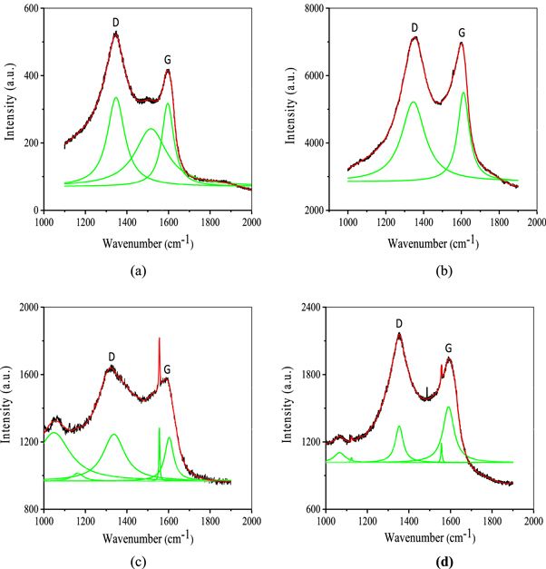
Figure 3. Raman spectras of DLC thin films deposited over substrates of (a) Si (b) Ti (c) Mo and (d) W materials using hollow anode in PF device.
Download figure:
Standard image High-resolution imageVisible Raman only has sufficient energy to excite sp2 vibrations, the higher energy of the UV Raman at 244 nm (5.1 eV) is required to excite vibrations from sp3 bonded carbon. Nevertheless, visible Raman can also be used to determine the sp3/sp2 fraction which has usually been extracted from shift or broadening of the G peak and also from the peak intensities ratio of D and G peaks as discussed in detail below. Other than that, the spike observed in Raman spectra [figures 3(b)–(d)] at around 1555 cm−1 could possibly be attributed to some unknown background source as its position was observed to be the same for all the samples. Moreover, it was also observed to be at the same position in the spectra recorded for some Raman inactive samples like metals.
The Raman spectra have been decomposed into two or more peaks using multiple Lorentzian peak fit. The number of peaks chosen for decomposition has been maximized in order to have reduced chi-square value and therefore proper fitting of the spectra. Various characteristics of these two peaks including the ratio of peak integrated intensities (ID/IG), full width at Half Maximum (FWHM) of G peak, G and D peak positions which signify different properties of DLC films are found to be varying for thin films deposited on different substrate. In general, a lower intensity ratio (ID/IG) can be interpreted as corresponding to higher sp3 content. However, values less than unity were reported even at the highly graphitized films [36]. The intensities of the D and G peaks calculated using the peak fitting of Raman spectra are not unique and it varies strongly with the choice of width and intensity of other nearby peaks. Hence, use of intensity ratio of two peaks may yield in erroneous estimation of sp3/sp2 carbon bonded ratio in the DLC thin films.
The FWHM and position of G peak have also been found to be strongly correlated to the fraction of sp3 bonded carbon atoms and the size of the sp2 bonded carbon clusters in films [35, 37]. The percentage fraction of sp3 bonded carbon (fsp3) in the deposited carbon thin films can be estimated using following equation: [37]

Here,
 G is the 'G' peak position in μm−1. The fraction of sp3 bonded carbon calculated using the above equation has been listed in table 2 along with various other characteristics of D and G peaks. The position of G and D peaks for DLC films deposited on various substrates viz Si, Ti, Mo and W were observed to be in the range 1590 cm−1–1611 cm−1 and 1337 cm−1–1353 cm−1, respectively. Variation in G peak position indicates different concentration of sp3 bonded carbons on different substrates and this has been calculated to be 16%, 8.7%, 13% and 18.9%, for DLC films deposited on Si, Ti, Mo and W substrates respectively.
Table 2. Characteristics of D and G peaks of Raman spectra of DLC thin films deposited on different substrates using hollow anode.
| Peak Positions (cm−1) | ||||||
|---|---|---|---|---|---|---|
| Anode | Substrate | D peak | G peak | G Peak width [FWHM (cm−1)] | Integrated Peak Intensity Ratio (ID/IG) | sp3 bond fraction (%) |
| Hollow anode | Si | 1347.3 | 1596.1 | 69.3 | 1.6 | 16 |
| Ti | 1345.8 | 1611.2 | 73.7 | 1.8 | 8.7 | |
| Mo | 1337.2 | 1603.1 | 51.1 | 2.7 | 13 | |
| W | 1353.3 | 1590.5 | 64.3 | 0.5 | 18.9 | |
As discussed earlier, DLC have been produced on rapid cooling or quenching of high energy precursor carbon ions on irradiation over relatively cold substrate surfaces (room temperature). Because of the pulsed discharge, the time available for any of the hybridizations (sp2 and sp3) to grow at the expense of others before the precursor carbon atoms are 'frozen' over the substrate surface (layer by layer) is too short and could depend upon thermal properties of substrate material. Hence, variation in concentration of sp3 and sp2 bonded carbon in DLC films deposited upon different substrate could be attributed to the difference in the thermal properties of substrates. In general, formation of sp3 bonded carbon is favored over other hybridization at high substrate temperature as also reported by Yadav V S et al [38]. Numerical calculations of surface temperature of different target material under pulsed ion irradiation have suggested that the temperature of the material irradiated to energetic ion beams from plasma focus rises fast (~10 K ns−1) up to a few thousand K and then rapidly cools down to room temperature [39]. The rate of rise in surface temperature and subsequent rapid cooling off strongly related to materials thermal properties. Hence, relatively low specific heat capacity (0.13 J g−1.K−1), high thermal conductivity (170 W m−1.K−1) and high melting temperature (3695 K) of W might have resulted into fast increase in its surface temperature to high value before its melting and subsequent cooling off rapidly, which, in turn favored more sp3 bonded carbon formation over it compared to those of formed over other substrates. Moreover, sp3 bonded carbon content on other substrates were found to be strongly correlated to their thermal conductivity i.e. substrate material having high thermal conductivity has high content of sp3 bonded carbon in the DLC films deposited over it. The widths of G peak have also found to be different for DLC thin films on different substrates as presented in table 2. The size of sp2 bonded carbon clusters was estimated to be maximum for Mo and minimum for Ti, respectively.
Surface morphologies of the DLC thin films over different substrates were observed to be different as revealed in plain view and cross section view of SEM images (figures 4–7). Microclusters of hybridized carbon atoms were seen to be formed on all the substrates. These microclusters were seen to be of different sizes distributed all over the substrate. The sizes of microclusters were measured to be in the range of a few hundred nm to a few μm. They could possibly have formed due to agglomeration of precursor ions of various kinds (C2H+, H+, C+n etc) on the substrate surface. The energetic precursor ions get cooled off on colliding with substrate at room temperature and transfers all its energy to substrate. This results into rapid increase in the substrate surface temperature. Enhanced surface temperature could possibly have escalated the combining of these precursor ions over the substrate. Hence, depending on the rise in substrate surface temperature, microclusters of different sizes were formed over different substrate.
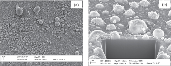
Figure 4. Plain view SEM image (a) and cross section view SEM image (b) of DLC thin films deposited over substrates of Si using hollow anode in the PF device.
Download figure:
Standard image High-resolution image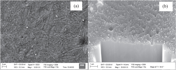
Figure 5. Plain view SEM image (a) and cross section view SEM image (b) of DLC thin films deposited over substrates of Ti using hollow anode in the PF device.
Download figure:
Standard image High-resolution image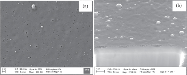
Figure 6. Plain view SEM image (a) and cross section view SEM image (b) of DLC thin films deposited over substrates of Mo using hollow anode in the PF device.
Download figure:
Standard image High-resolution image
Figure 7. Plain view SEM image (a) and cross section view SEM image (b) of DLC thin films deposited over substrates of W using hollow anode in the PF device.
Download figure:
Standard image High-resolution imageThese microclusters have appeared to be bright in SEM images which could be due to nanogranules of diamond (sp3 bonded carbon) formed within them. These nanogranules of diamond, being electrically insulating get electrically charged when exposed to focused electron beam during SEM characterization and produce more secondary electrons as well as fluorescence. Therefore, they can be clearly distinguished from other hybridized carbon atom clusters in the deposited films.
The wide variation observed in surface morphologies could be attributed to many factors including substrate surface physical conditions prior to thin film deposition and its thermal evolution on bombardment of energetic precursor ions. The important surface physical conditions prior to exposure to energetic precursor ion exposures are surface roughness, surface microstructure, and various other surface defects such as surface nodes among others. Evolution of these conditions over exposures to energetic precursor ions was mainly dependent of their thermal properties such as thermal conductivity, thermal expansion coefficients, melting temperature, etc [39]. Thickness of the DLC thin film was also measured using the cross section view SEM image and it was found to be around (274 ± 67) nm, (287 ± 54) nm, (236 ± 42) nm and (304 ± 63) nm, respectively, for films deposited on Si, Ti, Mo and W substrates.
Thin films of DLC have also been deposited on the Si substrate by inserting a graphite disc of size approximately 20 mm diameter × 40 mm long at the tip of the hollow anode [figure 1(b)]. Using graphite inserted anode, DLC thin film has been deposited on Si substrate using 200 plasma focus discharges by keeping all other parameters unchanged. The graphite was ablated on collision with the relativistic electrons, accelerated in post plasma focus disruption. This ablated graphite along with the energetic precursor carbon ions were deposited on the Si substrate placed at 10 cm axially above the anode tip. Hence, ablation of the graphite material provides carbon ions in addition to those from the carbon ions of acetylene precursor gas. Soh et al [24] have carried out the shadowgraphic studies of plasma focus dynamics and ablation of graphite for graphite inserted anode. They observed that the ablated material forms plasma plume near the anode tip and it moves towards the substrate along the anode axis. The ablated plasma plume remains collimated along the anode axis probably due to the its magnetic confinement by the azimuthal magnetic field due to discharge current that is there beyond plasma focus disruption. The collimation of the ablated plasma plume along the anode axis results in greater ablated ion energies (maximum energy of only a few tens of eV) and flux along the anode axis. Moreover, the energetic ions generated by m = 0 instabilities provides additional momentum along the anode axis to the ablated ions on collision with them.
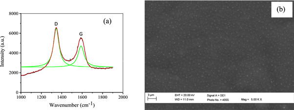
Raman spectra of DLC thin films deposited on Si substrate using graphite inserted anode has been obtained [figure 8(a)]. Typical characteristics of D and G peak have been derived from the multipeak fitted Raman spectra and its comparison with those for DLC films deposited using hollow anode has been tabulated in table 3. Using G peak position, the fraction of sp3 bonded carbon in DLC thin film was calculated to be 19.5% which is more than that of DLC thin films deposited without graphite insert. Moreover, the concentration of sp3 bonded carbon is found to be in line with that of 19% reported by Ghareshabani et al [21] for DLC deposited on Si substrate using 200 plasma focus shots of a low energy miniature repetitive plasma focus device. Increase in FWHM of G peak from 69.3 cm−1 to 73.4 cm−1 could be possibly due to decrease in sp2 cluster size. The possible reason of this could be quenching of deposited carbon layer by energetic precursor ions in subsequent plasma focus discharges.
Figure 8. Raman spectrum (a) and plain view SEM image (b) of DLC thin films deposited over Si substrate using graphite inserted anode in PF device.
Download figure:
Standard image High-resolution image
Table 3. Characteristics of D and G peaks of Raman spectra of DLC thin films deposited on Si substrates using hollow anode and graphite inserted anode.
| Peak Positions (cm−1) | ||||||
|---|---|---|---|---|---|---|
| Anode | Substrate | D peak | G peak | G Peak width [FWHM (cm−1)] | Integrated Peak Intensity Ratio (ID/IG) | sp3 bond fraction (%) |
| Hollow anode | Si | 1347.3 | 1596.1 | 69.3 | 1.6 | 16 |
| Graphite inserted anode | 1345.7 | 1589.2 | 73.4 | 1.63 | 19.5 | |
Surface morphology of DLC films has been shown in figure 8(b). It has revealed formations of micro-clusters similar to that formed using hollow anode [figure 4(a)], but, the gaps between the micro clusters have been bridged uniformly by the ablated graphite materials. The size of microclusters was in the range of a few hundred nanometers and it has been uniformly formed over the substrate. It is possibly because of the fact that a uniform layer of ablated graphite atoms covers the entire Si substrate in first few plasma focus discharges which in turns alters the substrate conditions for the precursor ions produced in the subsequent plasma focus discharges. Hence, use of graphite insert has helped in uniform deposition of DLC thin film over Si substrate with high sp3 bonded carbon content. Also, this has resulted into more thick DLC films of thickness around (387 ± 38) nm. Disadvantage of using graphite insert was that the ablated graphite got deposited all over experimental plasma chamber and on the plasma focus insulator surface along with those deposited on the substrate. This in turn unsettled the plasma focus operation as it required frequent dismantling of setup and frequent cleaning of plasma focus components. Hence, for deposition of high purity thin films at high deposition rate, proper selection of various parameters namely plasma focus anode material, anode geometry, substrate material, filling gas is required.
All the deposited films have been characterized using EDX. The EDX measurement confirmed the presence of carbon atoms along with impurity atoms from the erosion of plasma focus anode constituent material i.e. SS, and melting of substrate material. The concentrations of carbon atoms were measured to be different in the DLC films deposited on different substrates. Table 4 presents concentrations of carbon (at. %) in DLC thin films deposited over different substrates. Carbon atom concentration in the DLC films was measured to be 22.46, 22.7, 10.4 and 32 at.% on Si, Ti, Mo and W substrates, respectively when hollow PF anode was used. Moreover, the concentration of carbon on Si substrate was found to have increased to 56.74 at.% (Si = 42.49%, O = 0.48%, Fe = 0.1%, Cr = 0.15%) when graphite inserted PF anode was used. The reason for this has been attributed to the ablation of graphite by the high energy electron beam and then its deposition along with precursor carbon ions as mentioned earlier also.
Table 4. Elemental Composition (at.%) of DLC thin films deposited over various substrates using hollow anode.
| Substrate Material | ||||
|---|---|---|---|---|
| Element | Si | Ti | Mo | W |
| Si | 38.29 | — | — | — |
| Ti | — | 65.0 | — | — |
| Mo | — | — | 7.28 | — |
| W | — | — | — | 44.3 |
| C | 22.46 | 22.7 | 10.40 | 32.0 |
| O | 18.42 | 5.7 | 6.56 | 11.4 |
| Cr | 3.97 | 1.1 | 14.11 | 2.2 |
| Fe | 15.11 | 5.0 | 56.15 | 9.0 |
| Ni | 1.74 | 0.5 | 5.50 | 1.1 |
In addition to carbon, varying concentration of impurity elements such as Iron (Fe), Nickel (Ni), Chromium (Cr), and Oxygen (O) along with that from substrate materials have been measured in the different DLC thin films as presented in table 4. These impurities are due to erosion of plasma focus anode material i.e. SS304 by the high energy electron beams during post plasma focus disruptions and its deposition over the substrate. The concentration (at. %) of constituent elements of anode material i.e. Ni, Fe, Mn, Cr and C were measured to be 6.82, 62.93, 1.97, 17.22 and 11.06 at.%, respectively. Similarly, on exposure to high energy and high intensity precursor ions, substrate surface temperature rapidly increases to a few thousand deg. C and also beyond its melting point. This has already been confirmed through various observations and reported elsewhere [18, 19]. The melted surface layer intermixes with the precursor ions and gets deposited over it after cooling. All these contribute to the signals in EDX measurement. The impurities concentration can be significantly reduced by modifying the anode tip by using materials of high resistance to erosion e.g. Tungsten. The substrate can also be placed at off normal position to avoid direct interaction with energetic precursor ions.
4. Conclusions
Thin films of Diamond like carbon (DLC) have been deposited on four different substrate materials (Si, Ti, Mo and W) using a low energy operating plasma focus device. Each substrate was exposed to 200 plasma focus discharges performed at 2 kJ operation energy and 0.5 mbar filling pressure of acetylene gas. The characteristics of D and G peak of the DLC thin films were derived from their Raman spectra. The size of sp2 clusters was estimated qualitatively using the width of the G peak whereas fraction of sp3 bonded carbon has been calculated using the G peak position. Concentration of the sp3 bonded carbon has been calculated to be maximum (18.9%) and minimum (8.7%) for the DLC thin films deposited on W and Ti substrates, respectively. The concentration of sp3 bonded carbon for DLC thin films deposited on Si and Mo substrates was calculated to be 16% and 13%, respectively. The difference in sp3 bonded carbon concentration in DLC film deposited on different substrates has been attributed to the difference in substrate materials thermal properties specifically thermal conductivity, which, has resulted into different rate of increase in substrate surface temperature and subsequently rapid cooling down at different rates on exposure to energetic precursor ions. Surface morphologies of DLC thin films were observed to be different over different substrates. Thin films in form of microclusters of different sizes and shapes were observed to have formed over Si and W substrates whereas uniform and dense films were seen over Ti and Mo substrates. The difference in surface morphologies of the DLC thin films could be attributed to difference in substrate physical conditions prior to film deposition and further to its thermal evolution over the successive exposures to plasma focus discharges. Rise in surface temperature of different substrates to different values on exposure to energetic precursor ions may also have affected the surface morphology of the deposited thin films. The carbon concentration in different DLC thin films was also measured to be different, i.e., for DLC thin films on Si, Ti, Mo and W, the at.% of carbon was 22.46%, 22.7%, 10.4% and 32%, respectively.
DLC thin film on Si substrate has also been deposited using graphite insert at the anode tip. Due to graphite ablation, uniform and dense thin films of DLC have been observed to be deposited over Si. Also, the carbon concentration and sp3 bonded carbon concentration have been found to increase from 22.46 at.% and 16% to 56.74 at.% and 19.5%, respectively as compared to that of deposited using hollow anode. This demonstrates that the high purity, thick and uniform films of the required material can be deposited at high deposition rate just by inserting it at the tip of the plasma focus anode or simply attaching to the anode in the pellet form for ablation.
Acknowledgments
Authors are grateful to Dr T C Kaushik, former Head APD and Dr R K Rout, Raja Ramanna Fellow, BARC for fruitful discussion. We are thankful to Dr H K Poswal, HP&SRPD, BARC for his help in Raman spectroscopic measurement. We sincerely thank Dr Naveen N Kumar, MSD, BARC and Dr R Tiwari, Head MSD for their help in SEM characterization and EDX measurement.
Data availability statement
The data generated and/or analysed during the current study are not publicly available for legal/ethical reasons but are available from the corresponding author on reasonable request.