
Abstract
Piezoelectric inchworm actuators allow for a large stroke and high precision. This paper aims to minimize the footprint of the actuator by using semiconductor and MEMS fabrication techniques to build the frame and channel out of silicon wafers. The high precision of the semiconductor processes allows for precise tolerances as well as the ability to use batch processing for a shorter fabrication time. Using silicon as the mechanical material can also allow for the incorporation of the electrical signals into the frame.
Export citation and abstract BibTeX RIS
1. Introduction
Linear actuators are used in a vast number of applications that range from large scale, where the actuators exert a very large force, to very small, where the actuators are optimized for precision. The type of linear actuator used for a specific application will be determined based on the force, size, stroke, and step resolution of the actuator. Since these metrics can vary wildly across applications, there are multiple operating principles for the different types of linear actuators. These operating principles include but are not limited to hydraulic, pneumatic, rotary motor with a rack and pinion, and piezoelectric materials. Piezoelectric actuators are used in numerous applications due to their high precision, high force, and fast response [1–4]. Piezoelectric materials produce a voltage when a mechanical stress is applied or conversely mechanically deform with an applied electric field. The converse piezoelectric effect is described by the equation

where [dt ] is the matrix of the converse piezoelectric effect, [E] is the constant electric field, σ is the constant stress, and ε is the strain [5].
Piezoelectric materials have a very small strain per unit length. It is common for multiple layers to be placed on top of each other to amplify the deformation and these are referred to as piezoelectric stack actuators. Even with this increase in deformation, stack actuators have a displacement of approximately 0.1% of the total length. Direct piezoelectric actuators use this movement for nanometer resolution and a large force dependant on the size [1, 6]. The stroke is dependent on the length of the stack actuator, but it can be increased by flexible amplification [6]. Inertial drive piezoelectric actuators are driven with a periodic signal that expands then contracts the piezoelectric stack each cycle. Each cycle is used as an individual step and repeating steps can achieve a long linear stroke or rotational motion. There are multiple types of inertial actuators that string the individual steps together in their own way, including but not limited to impact drive and stick-slip piezoelectric actuators [1, 2, 6–8]. Impact drive actuators consist of piezoelectric material, a body, and an inertial mass. They are driven by a sawtooth waveform consisting of a slow ramp while actuating the piezoelectric material and a rapid ramp while returning to the original state. During the slow actuation, the inertial mass is extended with the friction holding the body in place. With the rapid shrinking of the actuator, the body breaks friction and slips forward creating a single step that can be repeated for longer motion [2, 6, 7]. Stick-slip actuators also take advantage of friction to move a slider/rotor depending if the design is for linear or rotary motion. The piezoelectric stack will move a fixture that contacts the slider or rotor and moves the piece due to the friction. After the piezoelectric stack is fully extended, it retracts to its original length breaking the friction with the slider/rotor. Stick-slip actuators differ from impact drive actuators because they move a slider or rotor with the piezoelectric stack staying in the same location while the entire piezoelectric stack moves with an impact drive actuator [2, 6, 7, 9].
In addition to inertial actuators, stepping actuators are able to achieve multiple steps to generate longer strokes than the size of the piezoelectric material can generate on its own. Stepping actuators, such as the piezoelectric inchworm, require multiple piezoelectric actuators used in sequence to achieve movement. Inchworm actuators can operate in either linear or rotary motion. There are multiple configurations of the linear piezoelectric inchworm actuator, including the walker, pusher, and walker-pusher designs [1–4, 7, 10–13]. The walker design allows for a stroke as long as the channel while maintaining the same clamp/blocking force throughout. The piezoelectric inchworm actuator uses at least three stack actuators operated in sequence to move throughout a channel. Figure 1 illustrates the sequence for movement to the right and by changing the order of the clamp actuators in the frame, the inchworm moves to the left. The piezoelectric actuators are shown red when extended.
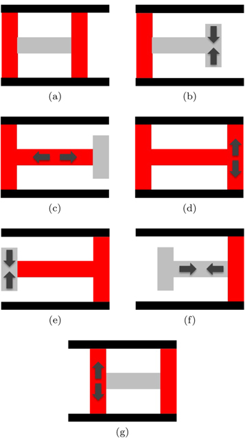
Figure 1. Inchworm Movement Sequence (a) both clamp actuators extended, (b) right clamp actuator relaxed, (c) step actuator extended, (d) right clamp actuator extended, (e) left clamp actuator relaxed, (f) step actuator relaxed, and (g) both clamp actuators extended.
Download figure:
Standard image High-resolution imageIn the piezoelectric inchworm walker design, the stroke of the actuator is determined by the length of the channel that the frame moves through. The required tolerance between the frame and channel is determined by the working stroke of the clamp actuators and the blocking force required on the channel. Mechanical amplification can be built into the frame that increases the clamp stroke from the actuator stroke, but would reduce the force exerted on the channel [4, 14]. When minimizing the footprint of the design, the tolerance is decreased with the reduction of the length of the clamp actuators. The piezoelectric inchworm walker actuator presented in this paper uses silicon as the mechanical material for the frame and channel. Silicon is chosen due to the significant processing capabilities developed in the microelectronics industry to achieve high precision at a fairly low cost. Silicon also allows for the possibility of the electrical connections to be built into the silicon frame negating the need for external wiring.
2. Design
The piezoelectric inchworm actuator presented in this paper is designed with miniaturization in mind. The size of the inchworm frame is dependent on the size of the piezoelectric stack actuator placed in the frame. The clamp actuators must be able to overcome the tolerance between the frame and the channel and exert forces on the channel. The stroke of the stack actuators is proportional to its length, so as the size is reduced, the maximum tolerance between the frame and channel is also reduced. Metal fabrication techniques, such as wire EDM, are able to achieve very tight tolerances [15], but it requires a long, expensive process to achieve the high tolerances. The frame and channel of the design shown in this paper uses silicon as the mechanical material which leverages the extremely high precision of semiconductor manufacturing processes to achieve the tight tolerances required for miniaturizing the piezoelectric inchworm actuator. This silicon frame has been designed using four piezoelectric actuators and is shown in figure 2. The step actuation uses two piezoelectric actuators instead of one. This design was chosen so that a stage can be attached to the top of the inchworm actuator in the middle of the frame and the addition of the stage would have a minimal effect on the actuator frame during movement. The size of the inchworm frame is 36.5 mm × 15 mm × 2.5 mm. The thickness of the frame is much larger than the thickness of standard silicon wafers, so multiple pieces are bonded together to achieve the thickness. Each piece of the frame and channel are the same except for the bottom piece of the frame has "feet" where the stack actuators are placed.

Figure 2. Inchworm frame.
Download figure:
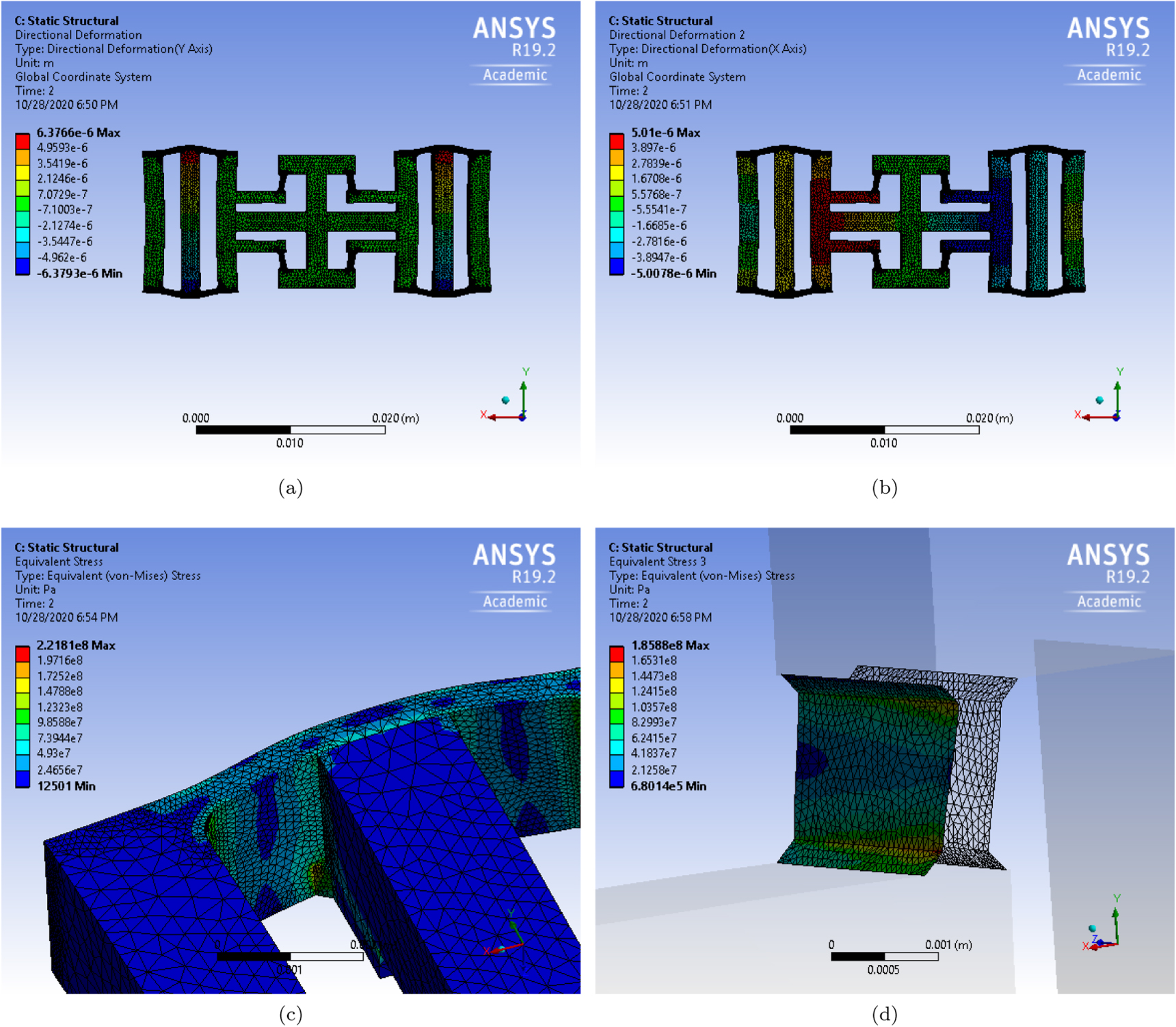
Standard image High-resolution imageThe piezoelectric stack actuators were sourced from a third party manufacturer, CTS Corp. The stack actuators chosen for the clamp and step actuators are from the NAC2011 family. The clamp actuators are 13.95 mm in length with a minimum tested free stroke of 13.2 μm and the step actuators are 7.2 mm in length with a minimum tested free stroke of 5.6 μm. Simulations are performed using Ansys Workbench using a single piezoelectric piece to model the forces of the piezoelectric actuators. The piezoelectric actuator was simulated so that the free stroke and blocking force matched the actuator specifications received from the manufacturer. The frame was simulated to determine the tolerances required for the design to operate, as well as the stress in the frame from operation. Figure 3 shows the deflection and stress with the maximum voltage applied to all of the actuators. Each side of the clamp has a simulated deflection slightly larger than 6.3 μm, which means the fabrication gap between the frame and channel must be less than 12.6 μm to operate. A smaller tolerance results in a larger force exerted on the channel increasing the blocking force of the silicon piezoelectric inchworm actuator. The channel was added to the model and the force reaction of a single side of the clamp was simulated at varying tolerances between the frame and channel. The simulated forces are shown in figure 4 and allows for a tolerance target based on the force requirement of the inchworm actuator. The step deflection of the actuator gives an idea of the individual step size of the actuator with the largest voltage applied. The step size of 2.87 μm was calculated by taking the average deflection of the end of each clamp actuator, since it is that area that makes contact with the channel. Figure 3 also shows the simulated Von-Mises stress in the frame due to the deflection from the piezoelectric actuators. The maximum stress due to the clamp actuators is less than 230 MPa and the largest stress is located on the area where the stack actuators are placed. The maximum stress due to the step actuators is less than 190 MPa which is slightly lower than the stress due to the clamp actuators. The overall stress from the static actuation of the piezoelectric actuators is less than the average bending strength for millimeter scale single crystal silicon from [16].
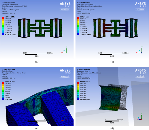
Figure 3. (a) Deflection in direction of clamp, (b) deflection in direction of step, (c) Von-Mises Stress on clamp flexure, and Von-Mises Stress on step flexure.
Download figure:
Standard image High-resolution image
Figure 4. Simulated force exerted on the channel versus tolearnce gap.
Download figure:
Standard image High-resolution imageThe desired velocity of the actuator will determine how fast the sequence of movements can be performed at a specific step size. Each actuator will have to fully deform in each part of the sequence, which is limited by two main constraints. The first is the minimum rise time on the piezoelectric stack actuator, which is discussed in the Drive Circuity subsection. The second is the maximum allowable frame stress due to the frequency of operation. Modal analysis simulations were performed using Ansys and figure 5 shows the first four modes of silicon frame with no boundary conditions. The lowest mode is at 5.967 kHz so the silicon frame can be driven below that frequency without problematic stress induced on the frame. Each of the modes show a larger deflection that then actuators can produce and certain boundary conditions, such as the channel itself, may not allow the frame to deflect in that mode either. These modes provide an idea of what frequencies might be an issue, although additional simulations are needed to better understand which frequencies will be problematic.

Figure 5. (a) Mode 1 at 5.967 kHz, (b) Mode 2 at 8.8054kHz, (c) Mode 3 at 11.195 kHz, and (d) Mode 4 at 14.658 kHz.
Download figure:
Standard image High-resolution image3. Fabrication
Silicon wafers are used to fabricate the frame and channel of this inchworm design. The thickness of each wafer used is 500 μm, so five pieces are needed for both the frame and channel. The fabrication for both the frame and channel are the same except for the method of aligning during bonding. Each silicon wafer is cleaned and a thermal oxide layer is grown. The frame or channel design is then patterned using photolithography. The exposed oxide layer is then etched in buffered oxide etch (BOE) to expose the silicon for Deep Reactive Ion Etching (DRIE). DRIE or the Bosch Process uses alternating isotropic etch and passivate cycles to achieve generally anisotropic etch [17–20]. These alternating cycles cause scallops on the sidewall and while the overall etch is generally anisotropic, it is not exactly 90°. More information on the DRIE process, scalloped edges, and sidewall angle can be found [17, 20].
During the etching process, the etched wafer is placed onto a backing wafer so that the pieces do not crack during etching. Once the etching process is finished, the pieces are released from the backing wafer, cleaned, and the oxide is removed. Figure 6 shows the top and bottom of the inchworm frame pieces after the DRIE process. It can be seen that the sharp corners of the top side are rounded and slightly jagged on the bottom side. Part of this can be attributed to the sidewall angle not being exactly 90°, but it is also believed to be due to fully etching through the wafer. The wafer that is etched is placed on a backing wafer to support the pieces mechanically as they are being etched. To fully etch all of the areas on the wafers, there will be places on the wafer that are fully etched before the etch process is complete. During these remaining etch cycles, reactive ions still impact these areas at the bottom of the channel which may cause the jagged edges.

Figure 6. Frame piece edges after DRIE on (a) top side and (b) bottom side of silicon frame piece.
Download figure:
Standard image High-resolution imageAfter the etched pieces are cleaned and the oxide removed, they are bonded together using Dyantex WaferGrip as the adhesive. The frame pieces are aligned and bonded together using a Karl Suss FC-150. The base pieces are also bonded using the WaferGrip, but are mechanically aligned using clamps. After bonding the excess WaferGrip is removed from the sides of both the frame and channel pieces. Finally the piezoelectric actuators are placed and attached with adhesive in the frame, shown in figure 7. Figure 8 shows the edge of the frame which illustrates that the bonding and etch processes can be further optimized.

Figure 7. Assembled piezoelectric inchworm frame.
Download figure:
Standard image High-resolution image
Figure 8. Edge of inchworm frame that shows alignment tolerance and sidewall angle.
Download figure:
Standard image High-resolution image4. Testing
The channel wafer is designed with three channels of different widths: 15, 20, and 25 μm larger than the width of the frame. These widths allow for larger bonding tolerances in both the frame and channel with worse alignment still functioning in the larger channels. The best results are from testing the frame in the smallest channel which shows good device fabrication and alignment during bonding. The step resolution is measured using an OptoNCDT 2300 by Micro-Epsilon. This laser sensor requires a flat surface which is perpendicular to the direction of movement. Since the channel surrounds the frame and does not allow for a straight line measurement to the frame itself, a piece of ceramic is attached to one edge of the frame to be used as the surface for measurement. The sensor is measuring the top of the ceramic piece and during the step actuation will displace more than the actual frame and vibrate for a short period of time before settling out at a single step. This can be seen in the data in the Results section. Figure 9(a) shows the pieces needed for operation including the DC power supply, drive circuitry, microcontroller, and PC. Figure 9(b) shows the setup for measuring the individual step size, including the ceramic piece attached to the inchworm frame. As previously stated, the ceramic piece is required as the measuring surface for the sensor. Due to how the ceramic piece is attached, it will oscillate like a end-clamped cantilever beam during actuator motion but will eventually settle due to the air resistance. The magnitude of motion is much more than the actual frame, which can be see in the step resolution data in the Results section.
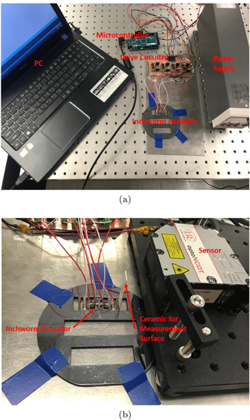
Figure 9. Testing setup for piezoelectric inchworm actuator: (a) all components required for operation and (b) measurement of step sizes.
Download figure:
Standard image High-resolution image4.1. Drive circuitry
The piezoelectric stack actuators act electrically as a capacitor and must be charged with a voltage to produce the mechanical deformation needed for the actuator to operate. Figure 10 shows the circuitry to control the voltage for a single piezoelectric stack actuator. The supply voltage is generated using Keithley 2260B-800-1 DC power supplies. A NMOS transistor is used to charge and discharge the piezoelectric actuator and the resistor RS is used to limit the current while charging/discharging. The NMOS transistor is controlled by a PWM signal from a microcontroller. The voltage is applied to the actautor when the transistor is off and the actuator discharges to zero voltage when the transistor is on. The left side of the circuitry turns off the supply voltage before the stack actuator discharges to minimize current while the actuator is discharging. The resistors R1 and R2 are for biasing the NMOS and PMOS transistors based on the supply voltage. The piezoelectric inchworm actuator was tested for step resolution using a 10 kΩ resistor for RS so that each actuator charge/discharge was 10ms. The supply voltage is turned on/off 10 μs before the PWM signal charging/discharging the piezoelectric actuator and adds to the total time of a single actuation bringing it to 10.01 ms. The velocity of the PIA was tested using five different resistors for RS, a 10 kΩ, 5 kΩ, 1 kΩ, 500 Ω, and 100 Ω. This results in a the time for the single actuation time of 10.01 ms, 5.01 ms, 1.01 ms, 0.51 ms, and 0.11 ms respectively for each of the resistors tested. As the resistor RS is decreased, the charge/discharge time of the actuator is decreased while increasing the current demand from the supply voltage. Other options for charging the actuators, such as using charge pumps are described elsewhere [21]. Since there are six piezoelectric actuator movements for a single step, the actuator is tested at a frequency of 16.6Hz for the 10 kΩ resistor, 33.2 Hz for the 5 kΩ resistor, 165 Hz for the 1 kΩ resistor, 326 Hz for the 500 Ω resistor, and 1.51 kHz for the 100 Ω resistor, all below the first mode simulated in the Design section.

Figure 10. Drive circuitry for a single piezoelectric stack actuator.
Download figure:
Standard image High-resolution image5. Results
The inchworm actuator is tested for step resolution and velocity, although the velocity is limited by the drive circuitry. Since the setup for testing will induce vibration in the ceramic piece, there is a one second lag between steps for the vibration to settle out to test the step resolution. The clamp actuators are driven at 148V, slightly below the maximum voltage for the piezoelectric stack actuators. The step actuators are driven at 148V as well as at every 20V interval between 20V and 140V. One may notice that once the actuator starts or changes direction, the step displacement varies but it stabilizes after a few steps. This variation may be due to the actuator needing to build the inertia in a particular direction and overcoming any friction in the channel. Due to this step variability, the data is plotted after a multiple steps of the PIA once it has started or the direction has changed. Movement towards the sensor is recorded as a negative value and the plots show each step as a negative displacement. The actuator is tested twice at each voltage moving 125 steps in the direction towards the sensor. The first 25 steps of each test were ignored to allow the step displacement to stabilize. During the tests, the actuator has larger step sizes toward the sensor, than away from the sensor. The ceramic piece on the edge may account for some of this, but probably the contributing factor in the step size differences per direction is that one clamp exerts more force on the channel than the other. Tests performed with the sensor measuring the other side of the inchworm frame show similar results with regard to one clamp being more effective than the other. Figure 11 shows the displacement measurements for steps at different voltages: (a) shows the displacement data for the different voltages applied to the step actuators, (b) shows the mean of the step sizes operated at the different voltages with the standard deviation indicated by the error bars. The data plotted for the mean step size and standard deviation was taken at the end of the 1s pause to try and mitigate the vibration of the ceramic piece. The mean value of step size at the different voltages is fairly linear and consistent throughout the higher voltages. When the step actuators were being driven with 20V, there is more variation in each step size than the other voltages tested, with certain steps showing movement in the wrong direction. It is believed that the deviation in initial cycles, as well as the inconsistency of the 20V steps, is due to the friction in the channel. The maximum step size is larger than the simulated step size which is partly due to the piezoelectric actuators having a larger stroke than predicted in simulation.
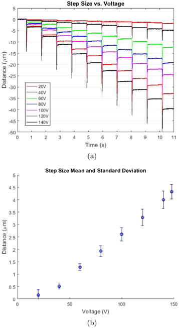
Figure 11. Step resolution data of the piezoelectric inchworm actuator: (a) sensor data during operation and (b) calculated mean with standard deviation error bars.
Download figure:
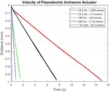
Standard image High-resolution imageFigure 12 shows the velocity test data of the piezoelectric inchworm actuator. The velocity of the PIA is tested by operating the step actuators at the maximum voltage (148V) with varying resistors limiting the current to each stack actuator. The driving frequencies of 16.6 Hz, 33.2 Hz, 165 Hz, 326 Hz, and 1.51 kHz are tested with each corresponding resistor for a total of 250 steps. The distanced covered by each test differs slightly, which is due to each step not being exactly equal, but the velocity is 0.65 mm/s, 0.13 mm/s, 0.63 mm/s, 1.23 mm/s, and 6.3 mm/s for the respective frequencies. During the testing at the frequency of 1.51 kHz, there was more slipping of the actuator during tests than any other frequency. While this frequency did not cause damage to the actuator, it may be too large for consistent steps of the piezoelectric inchworm actuator.
Figure 12. Velocity data of the piezoelectric inchworm actuator.
Download figure:
Standard image High-resolution image
6. Conclusion
This paper presents a piezoelectric inchworm walker actuator with the frame and channel fabricated from silicon wafers. This allowed for a small footprint, 36.5 × 15 × 2.5 mm, without expensive and long metal fabrication techniques. The prototype was successfully tested and achieved a mean step size at the maximum voltage of the step actuators of 4.32 μm and sub-micron step sizes at 40V and below. The friction within the channel causes a large standard deviation of the step sizes along with non-consistent steps when started or switching directions. The friction within the channel can be reduced by optimizing the fabrication processes such as DRIE and bonding the pieces together. A wear resistant material may be required to reduce any chipping of the silicon where the contact is made by the clamps. Using silicon as the mechanical material also allows for the integration of wiring and other electrical signals into the frame which is currently being pursued through follow-on efforts.
Acknowledgments
I would like to thank Robert Wortman at the Microelectronics Department at L3Harris, the Alabama Micro/Nanoelectronics Science and Technology Center, Paul Koeneman, Thomas Stegeman, Amanda Cipriano, Vaibhav Gupta, Brent Bottenfield, and Sherman Peek. This work was supported by L3Harris.