
Abstract
In superconducting radiofrequency accelerating cavities for particle accelerators, the Nb/Cu structure is one of the alternatives to bulk Nb but R&D is required to achieve a reproducible performance that competes with bulk Nb. The DC entry field Hen and critical temperature were studied in the thin Nb films deposited by magnetron sputtering on Cu substrate. The Nb surfaces were further treated by Nd:YAG laser at four energy doses (D1 = 350, D2 = 233, D3 = 175 and D4 = 140 J cm−2). The superconducting properties and other characteristics obtained by atomic force microscope, scanning electron microscope and x-ray diffraction were compared before and after laser treatment. The laser treatment increased the field of first flux entry by up to 65% compared to a non-irradiated sample. The laser irradiation also led to reduction of surface roughness, improvement of the surface morphology, reduction in crystallite size and increase of lattice parameter.
Export citation and abstract BibTeX RIS

Content from this work may be used under the terms of the Creative Commons Attribution 4.0 licence. Any further distribution of this work must maintain attribution to the author(s) and the title of the work, journal citation and DOI.
1. Introduction
Superconducting radiofrequency (SRF) cavities are devices which are used in particle accelerators to accelerate and manipulate charged particles. The most common material used in SRF cavities is bulk Nb due to its highest lower critical field Hc1 = 180 mT (at 0 K) and highest critical temperature Tc = 9.25 K of all pure elements [1, 2]. The SRF cavities operate in a Meissner state with high field performance reduced when the magnetic component of the RF field begins to penetrate the inner surface of the cavity (transition to a mixed state leading to an increase of Ohmic losses) [3]. Thus, the operating limit of the SRF cavity is reaching the so-called first magnetic flux entry field Hen [4].
However, as the performance of the bulk Nb in accelerating cavities has almost reached its theoretical limits [5], employing high purity (400 < RRR < 900) and large grain (∼5–10 cm) Nb, mechanical and chemical surface polishing, bakeout and other post-production treatments. One of the promising alternatives is a thin film of Nb deposited on Cu substrate. Creation of the Nb/Cu structure provides technological and cost advantages compared to bulk Nb, in particular better thermal stability provided by the large thermal conductivity of the Cu, higher mechanical stability, reduced sensitivity to Earth's magnetic field trapping or absence of undissolved inclusions [6]. At 4.2 K and low accelerating fields, the benefits provided by Nb film over Cu make this technology extremely competitive with bulk Nb, finding application in several accelerators [7–10], but this approach has not yet achieved the performance of bulk Nb cavities at high accelerating fields [6]. The structure and morphology of deposited Nb films is different from the bulk Nb: the grain size is much smaller (<3 µm). Thus the innovations in materials as well as treatment technology are required for the new generation of the SRF cavities.
It is well known that the surface of the superconductor provides a barrier against the field penetration [11, 12] and therefore the surface quality of the inner wall of the cavity has a significant impact on its performance [13, 14]. Defects such as microscopic roughness and pitting occurring on the cavity surface can cause enhancement of the local magnetic field and premature flux penetration [15–17]. The improvement of the Nb surface can be achieved by mitigation of the surface defects [18] with a small, disordered Nb grains, and slightly strained lattice parameters [19]. One of the promising solutions to improve the Nb structure and reduce the surface roughness is using laser irradiation which has already been used for the bulk Nb [20, 21] as well as for thin Nb film on Cu [22–24].
In this work, we have investigated structural and superconducting properties of small planar Nb/Cu samples before and after irradiation of the Nb film surface with laser, at several laser light intensities. The superconducting properties were determined at 4.22 K temperature in a DC magnetic field oriented parallel to the sample face, in order to investigate the basic effects of the laser irradiation on the Nb film. Some portion of the results presented in this work was published in [25] but no explanation was given there. It should be noted, however, that these results are initial and only preliminary in respect to the SRF cavity applications, because the conditions that the superconducting thin films are exposed to in the RF cavities are quite different.
First of the substantial differences stems in the fact that the magnetic field in the RF cavity, applied to the surface, exists only on the outer side of the film, no field is present on the substrate side. There are a few methods to address this problem, each of them involving specific experimental challenges, like the requirement for a homogeneous coating of special elliptic-shaped samples [26]. Other of these methods are based on a local probing of planar sample with AC applied magnetic field, detecting the onset of the field penetration in the 3rd harmonic component of the response voltage [27, 28]. If a DC applied magnetic field is used, the full penetration of the applied field through the thin film is detected by means of a Hall probe [29–31].
Another obvious difference comes from the fact that all the presented measurements were performed in DC magnetic field, while AC fields with the frequencies in the range of MHz and GHz exist in the RF cavities. Thus, the conclusion on how laser treatment affects the superconducting cavity performance could only be drawn in the final test at the RF conditions. This work aims at identifying the most promising laser treatment process and at understanding the main tendencies and correlations between the laser parameters, film microstructure, surface morphology and the DC superconducting properties.
2. Experimental
2.1. Sample preparation
The production process of the sample started from the high purity 2 mm thick oxygen-free electronic copper sheet (rolling machined) which was cut to size of 53 × 53 mm2 [32]. In the Nb film production process a great attention was paid to the preparation of the Cu substrate because its roughness and morphology are expected to be replicated by the growing Nb film.
The Cu surface preparation consisted with a two-step polishing process; first by electropolishing (EP) and then by chemical polishing with SUBU5 for a short time. Both polishing procedures were already used in the past for substrate preparation in Nb films for SRF cavities [7, 33]. The two-step polishing approach was used to follow current LNL (Legnaro National Laboratory) protocol of 6 GHz cavity treatment that includes SUBU5 polishing as a final polishing step. The use of SUBU5 allows obtaining a mirror-like surface, but it creates pits on the surface which are caused by the oxygen released from the hydrogen peroxide attacking the metal surface [34, 35]. Thanks to shorter treatment in the SUBU5 solution, the use of the two-step process in principle allows to maintain the mirror-like surface and reduces the amount and dimensions of the pitting holes [36]. It should be noted that from the beginning of our aim was to test the industrial scale substrate polishing procedures that are able to treat the full-size of SRF cavities. We have not optimized the polishing procedures to prepare small planar samples of the best possible surface quality.
The electrolyte used for EP was a mixture of phosphoric acid and n-butanol in a volume ratio of 3:2, at room temperature, without bath agitation. The SUBU5 polishing solution consisted of sulfamic acid (5 g l−1), hydrogen peroxide 32% (50 ml l−1), n-butanol 99% (50 ml l−1) and ammonium citrate (1 g l−1) at a working temperature 72 °C. The treatment protocol included instant passivation of the copper after SUBU5 treatment to ensure oxide-free surface. Passivation was made by inserting the sample into a prepared solution of 10–15 g l−1 of sulfamic acid. The etched thickness removal after the EP process was 36.8 µm and after the SUBU5 solution was 8.7 µm. The total thickness removal from the Cu surface after a two-step polishing process was then 45.5 ±1 µm.
After the polishing processes, the substrate was coated with a 3 μm thick Nb film by magnetron sputtering in argon discharge gas. The parameters set to produce the Nb film are shown in table 1. Standard polishing protocol for the Cu substrate and more information about Nb deposition process are in detail described in [32] (L16 sample).
Table 1. Nb deposition parameters set to produce the Nb film.
| Parameter | Value |
|---|---|
| Substrate heated | 650 °C for >40 h |
| Base pressure at 650 °C on a substrate | <9 × 10⁻⁸ mbar |
| Current density | 27 mA cm−2 |
| Target power | ≈750 W |
| Discharge gas pressure | 5 ×10⁻³ mbar |
| Deposition time | 20 min |
| Deposition rate | 150 nm min−1 |
2.2. Laser post-treatment
After Nb film deposition, five planar samples with almost identical dimensions (∼2 × 2 mm2) were cut from the deposition sample using a laboratory cutting machine with a SiC cut-off disc. Four of them were irradiated by pulsed laser light using different energy doses.
The Q-switched pulsed Nd:YAG laser (model: NL301G, produced by Ekspla, Lithuania) was used in the post-treatment process of the Nb film affecting its surface. The following parameters were used for laser irradiation: wavelength λ= 1064 nm, intensity I= 200.0 MW cm−2, repetition rate of ν= 10 Hz, beam profile 'hat-top', beam diameter d = 1.5mm and the pulse duration of the laser τ = 6 ns. The laser irradiation was performed at room temperature in an argon atmosphere under pressure 1.1 × 10⁻⁶ Pa. Scanning of the laser beam was performed normally to the Nb surface with the constant hatch distance 0.3 mm. Different scanning speeds of the laser (v1 = 0.2, v2 = 0.3, v3 = 0.4 and v4 = 0.5 mm s−1) resulted in different energy doses applied on the Nb surfaces: D1 = 350 J cm−2, D2 = 233 J cm−2, D3 = 175 J cm−2 and D4 = 140 J cm−2. The laser parameters used in this paper were chosen according to earlier study [22] in which the changes in structural properties of the Nb/Cu samples were in detail studied after laser irradiation.
Every laser pulse generated the same energy ∼21 mJ and the samples absorbed thermal incident energy 8.4 mJ due to ∼60% reflection (figure 1). Therefore, the thermal energy of a single laser pulse is the same for each dose. The number of laser pulses at the same spot (dose) has an accumulation character and influences the crystallinity of the material, decreases surface roughness, and improves adhesion Nb to Cu upto 36% according to [22]. These processes take place due to the inhomogeneous distribution of thermal energy in the Nb film. The gradient of temperature with the maximum at the surface, during a laser pulse, takes place. Calculation of temperature distribution in Nb/Cu structure during the laser pulse is presented in [22].
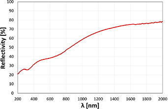
Figure 1. Reflectivity of the non-irradiated Nb surface as a function of applied light wavelength from infrared to ultraviolet. At the wavelength of the applied laser light (1064 nm) the reflectivity is approximately 60%.
Download figure:
Standard image High-resolution image2.3. Nb film characterization
The surface roughness Ra of the Nb films was determined using the NTEGRA prima atomic force microscope (AFM) in tapping mode with a HA_NC measurement probe from NT-MDT spectrum instrument. Before the AFM measurements, the samples were cleaned in an ultrasonic bath of liquid isopropanol for 2 min, then rinsed by acetone and finally dried by nitrogen gas. The surface roughness and corresponding standard deviation were calculated from the average value of four measurements performed on different spots on each sample's surface. Scan areas were for all measurements set to 10 × 10 µm2 with 256 × 256 scan points, scan velocity was 5.6 μm s−1 with a scanning step 29.22 nm.
The surface morphology of the Nb films was observed using FEI quanta 250 FEG scanning electron microscope (SEM). The reflectivity of the sample was characterized by SolidSpec-3700 UV-VIS-NIR spectrophotometer from Shimadzu. The x-ray diffraction (XRD) was measured using Bruker AXS-D8 discover super speed diffraction system.
2.4. Superconducting properties
Critical temperatures (Tc), first magnetic flux entry field (Hen) and full penetration field (Hp) of the Nb films were characterized using vibrating sample magnetometer (VSM) option of the commercial physical property measurement system from Quantum Design Inc. The measurements were performed at the sample temperature of 4.22 K in an applied magnetic field oriented parallel to the flat face of the samples with accuracy of ±1°. The DC magnetization curves were measured after cooling the sample below Tc in zero applied field. The magnetic moment (m) of the sample was then measured in dependence on the increasing applied magnetic field (Ha) at a constant speed 0.2 mT s−1, recording the initial magnetization curve (figure 2).
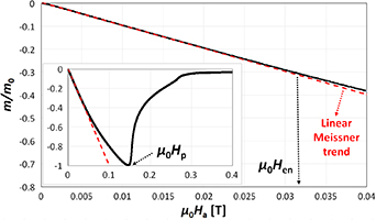
Figure 2. Initial magnetization curve of the non-irradiated sample normalized to maximum magnetic moment m0 (in absolute value) illustrating determination of the Hen and Hp characteristic fields.
Download figure:
Standard image High-resolution imageThe first magnetic flux entry field Hen represents the applied field at which the magnetic flux starts entering into the sample's volume. It was detected as the applied field at which the initial magnetization curve starts to deviate from the linear dependence that the curve follows in the first part starting from the zero applied fields [37, 38]. The field Hen was determined employing a 2% relative difference criterion, i.e. as the applied field at which the relative difference between the magnetization curve and the linear Meissner trend reaches 2%. The choice of the criterion is arbitrary as the deviation of the sample magnetic moment from the linear Meissner trend is smooth and continuous.
Main goal of our study was to compare the superconducting properties of the laser-irradiated films between each other by the same measurement technique as we used in [39]. The Hen values reported here relate to the applied magnetic field and are not corrected for the geometrical effects. They are smaller than the physical first magnetic flux entry field that refers to the field at the sample surface. The field experienced at the sample surface is amplified with respect to the applied field Ha due to geometrical effects. These effects are connected with the fact that sample of finite dimensions is immersed in applied magnetic field (demagnetization effects) and with field enhancement near the sample edges. Analytical study [40] allows estimating the geometrical field enhancement factor to a certain extent. Here, an infinitely long rectangular bar in a transverse applied field is considered, representing an idealized 2D approximation of the VSM sample geometry. For our sample dimensions (aspect ratio ∼0.002) the analytical results show that the field at the flat face surface is practically equal to Ha and at the narrow face surface (sample edge, perpendicular to Ha) the field reaches the value 2Ha in a distance d of approximately d = 0.025 × (Nb − thickness) from the edge, increasing when approaching closer to edge. Hence, the geometrical field enhancement factor could be estimated to a value of approximately two for our samples. In the VSM experiment, both the substrate–Nb interface and the 'top' surface of the Nb film (Nb–air interface) are exposed to the applied magnetic field. We assume, however, that the quality of the Nb surface at the substrate side is much higher than at the top surface and the field penetration thus starts at the top Nb surface.
Another characteristic determined from the initial magnetization curves was the applied field at which the minimum magnetic moment (maximum in absolute value) in the initial magnetization curve is reached, Hp (figure 2). It is proportional to the full penetration field. The Hp value is one of the indicators of the overall strength of flux pinning in the sample, a higher difference between Hen and Hp indicates a stronger pinning. In an ideal pin-free sample one would have Hen = Hp, and further Hen = Hc1 if no geometrical factors were involved.
3. Results and discussions
3.1. Samples
Figure 3(a) shows the surface of the Cu substrate (53 × 53 mm2) after application of the EP. The surface has a mirror-like appearance with visible diagonal texture due to oxygen generation during the polishing process in absence of bath agitation [32, 36]. The application of further chemical polishing using the SUBU5 process (figure 3(b)) reduced the texture, but did not remove it completely. Figure 3(c) shows the sample after deposition of the thin Nb film that has similar optical appearance like the Cu substrate (sample in this figure shows a cut of approximately one quarter of the initial size). The surface features like the diagonal texture are to a great extent replicated in the surface of the deposited Nb film.
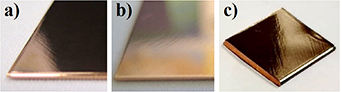
Figure 3. (a) The surface of the Cu substrate after EP process. (b) The Cu surface after the second chemical polishing process (EP+SUBU5). (c) The surface of the sample after deposition of the Nb film.
Download figure:
Standard image High-resolution imageFigure 4(a) shows SEM micrograph of the Cu surface after application of the both polishing processes (EP+SUBU5). The non-uniform distribution of pits observed on the Cu surface was caused by the application of SUBU5 process. The SEM micrograph of the Nb film before laser irradiation is shown in the figure 4(b). It shows a corrugated morphology related to polycrystalline structure with a size of grains 0.5–3 µm. Pits observed on Cu substrate are replicated on the Nb surface after deposition, with similar diameters, ranging from 0.2 to 2 µm. The grain boundary is very clear without annealing and gradually disappeared as the laser dose increased (figures 4(c)–(f)), similar as observed in [23].

Figure 4. SEM micrographs of: (a) Cu surface after EP+SUBU5 treatment. (b) Nb surface before laser irradiation. (c) Nb surface after laser irradiation by dose D4 = 140 J cm−2, (d) D3 = 175 J cm−2, (e) D2 = 233 J cm−2 and (f) D1 = 350 J cm−2.
Download figure:
Standard image High-resolution imageFigure 4(c) shows Nb surface after laser irradiation by the lowest dose D4 which was visibly melted. Some level of the initial corrugation is still presented after laser irradiation. The pitting is no more presented on the Nb surface indicating that the pits were filled by melted Nb. To some extent similar corrugation can be observed on the surface irradiated by dose D3 (figure 4(d)), but with visibly smaller dimensions. No pitting present at the D3 surface was observed as well. The samples irradiated by doses D2 and D1 look well smoothed with practically complete removal of the initial corrugation (figures 4(e) and (f)). However, small holes emerged in both cases, with diameters from approximately 0.1 µm to about 1 µm. Similar features were also observed in [22, 24] after laser irradiation. Possible explanations could be connected with melting, or even boiling of the Cu under the Nb film, also known as subsurface melting or lid effect [41]. Ejection of rapidly expanding molten Cu can create these holes in the solid Nb film. Melting or boiling of the Cu under the Nb film can occur during the thermal action of the laser because of non-uniform thickness of melted Nb film. Moreover, the boiling point of Cu is only 84 K higher than the melting point of Nb (melting temperature of Cu is  = 1357.8 K, boiling temperature of Cu is
  = 2835 K, melting temperature of Nb is
  = 2741 K).
3.2. Surface roughness of Nb films
The surface roughness Ra of the Nb films, determined from the AFM measurements, is summarized in table 2. The laser treated samples show a significant reduction of the surface roughness compared to the non-irradiated sample, reduction by approximately one half can be observed in all cases. Disappearance of the pitting and somewhat persisted corrugated morphology resulted in reduced surface roughness after laser irradiation by doses D4 and D3. The surface roughness of the samples irradiated by doses D2 and D1 combines the positive effect of practically complete removal of the initial corrugation with the negative contribution of holes resulting in weaker increase of Ra compared to D3 sample. This reflects that melting of the Nb surface occurred after laser irradiation resulting in a smoother surface which was also observed in the earlier works [20–23].
Table 2. Microstructure and DC superconducting properties of Nb thin film before and after laser irradiation.
| Energy dose | a (nm) | Ra (nm) | L-vol (nm) | Crystalline size (nm) | μ0 Hen (mT) | μ0 Hp (mT) |
|---|---|---|---|---|---|---|
| Non-irradiated | 0.329755  0.000003 0.000003 | 14.9  2.1 2.1 | 203  7 7 | 26.4 | 31.0  1.5 1.5 | 145 |
| D4 = 140 J cm−2 | 0.32999  0.00002 0.00002 | 8.8  1.9 1.9 | 40  2 2 | 20.2 | 46.8  2.3 2.3 | 145 |
| D3 = 175 J cm−2 | 0.32998  0.00001 0.00001 | 6.4  1.3 1.3 | 35  1 1 | 20.6 | 51.0  2.5 2.5 | 144 |
| D2 = 233 J cm−2 | 0.329823  0.000006 0.000006 | 8.3  1.5 1.5 | 54  1 1 | 20.1 | 38.2  1.9 1.9 | 143 |
| D1 = 350 J cm−2 | 0.32995  0.00003 0.00003 | 7.5  2.0 2.0 | 43  5 5 | 19.7 | 39.4  2.0 2.0 | 145 |
3.3. XRD measurement
The XRD patterns of the investigated samples are shown in figure 5. The Lattice parameter (a), crystalline size and volume weighted mean column height parameter (L-vol) were obtained from XRD data for all investigated samples (table 2). In the evaluation process, a completely homogeneous sample was assumed and all maxima of a given phase were taken into account.
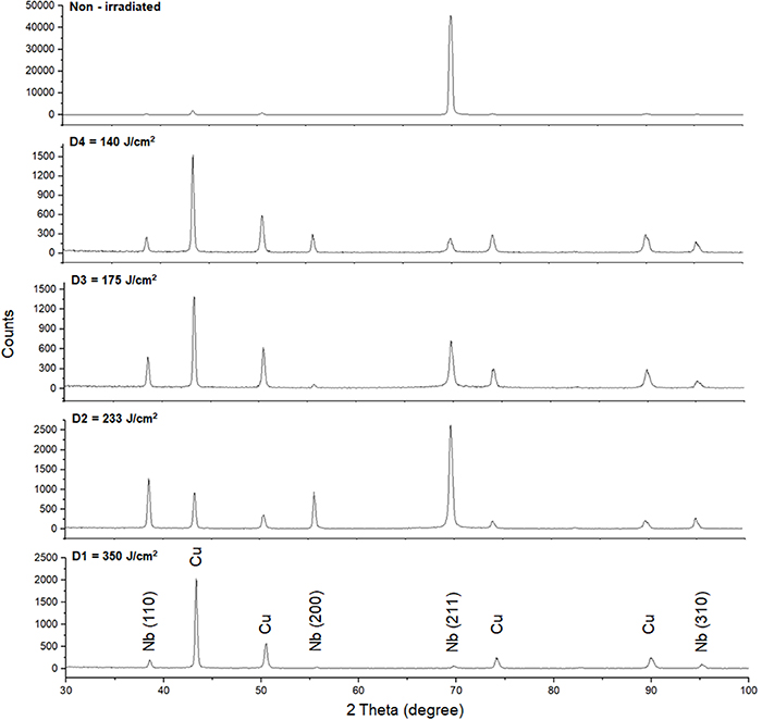
Figure 5. The XRD patterns of the non-irradiated sample and the samples irradiated by the laser doses D1–D4.
Download figure:
Standard image High-resolution imageThe XRD pattern of the non-irradiated sample shows presence of a dominant diffraction maximum at 70° 2θ and weak reflections of other orientations at lower and higher angles. There is a strong orientation in Nb (211) resulting in one order of magnitude larger L-vol parameter compared to samples irradiated by laser. The lattice parameter of the non-irradiated sample exhibits a = 0.329755  0.000003 nm. Strong orientation in (211) and observed Nb grain size reflect hetero-epitaxial texture of the Nb driven by the underlying Cu structure typical for oxide-free films [6].
After the laser irradiation, the initial orientation of Nb crystallites disappeared and new ones entered with a random orientation in all four cases. Size of Nb crystallites, calculated using the Scherrer equation [42], decreased from 26 nm to about 20 nm after laser irradiation. This reflects that recrystallization was probably only in the first phase—nucleation and subsequent limited growth of new crystals. As the size of crystallites is very sensitive to the recrystallization time and temperature, the new Nb crystallites became finer due to short laser pulses (τ = 6 ns) and very fast heat dissipation into the copper. This reflects that rapid solidification occurred after laser irradiation, so that more nucleation centres were formed and finer Nb crystalline structure was created.
The laser irradiation caused a weak increase in the lattice parameters observed in all four cases up to a = 0.32999  0.00002 nm (∼0.08% increase at maximum). The increase of the lattice parameters can be explained by the relaxation of the residual intrinsic compressive stress, considering the lattice parameter of the Nb with zero stress a0 = 0.3300 nm [43, 44], which was also observed in [24] after laser irradiation.
3.4. Superconducting properties of Nb films
The critical temperatures have been determined from the temperature dependence of the sample magnetic moment in the constant magnetic field of 5 mT, applied parallel to the sample flat face. The magnetic moment was measured from initial temperature T = 12 K decreasing to T = 4.22 K in a 0.05 K recording step with a sweep rate of 0.25 K min−1. The superconducting transition temperature Tc was determined as the onset of magnetic moment change. Figure 6 shows the normalized magnetic moment as a function of temperature for all investigated samples.
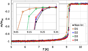
Figure 6. Normalized magnetic moment as a function of temperature for all investigated samples. The m5K represents the magnetic moment at T = 5 K. The inset shows a start of the transition to superconducting state.
Download figure:
Standard image High-resolution imageThe critical temperature of the non-irradiated sample is Tc = 9.3  0.05 K, comparable to typical value of the bulk Nb. After the laser irradiation, the critical temperature decreased slightly in samples irradiated by doses D2 and D4. Somewhat larger difference in Tc was observed in the samples irradiated by doses D1 and D3. However, the change is not very significant, 0.2 K at maximum between the non-irradiated sample and that of irradiated by laser dose D1. These reductions in Tc could be explained by the increase in lattice parameters [45] or due to contaminants which entered the surface after laser annealing [23]. This scenario is possible if the contamination was not systematic in all cases but occurred by random way mostly in samples D1 and D3. However, the observed reduction in Tc was not significant and there is no correlation with the laser dose applied on Nb surfaces or changes in Hen after laser irradiation.
The superconducting properties of the Nb films were analysed from the initial magnetization curves (figure 7) and magnetic hysteresis loops (figure 9). Figure 7 shows initial magnetization curves normalized to the maximum absolute value of the moment m0. As one can see, each curve has slightly different behaviour until the reaching the maximum magnetic moment, where the curves merge at almost identical field value of Hp (table 2). At applied fields higher than Hp, the curves overlap and continue with almost identical behaviour up to the field Hc2 which is also identical for all of the samples (μ0 Hc2 ∼ 0.3 T).
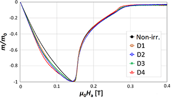
Figure 7. Normalized initial magnetization curves of all the investigated samples.
Download figure:
Standard image High-resolution imageFigure 8 shows initial magnetization curves normalized to linear Meissner trend (mMeiss) as a function of external applied magnetic field for all investigated samples. This graph represents the size of the applied field which starts to penetrate into the sample´s volume as a deviation of the curve from its constant initial value. The later the deviation of the curve from its constant level, the higher the value of Hen. As we can see, the use of a laser irradiation resulted in an increase of Hen values in all four cases. The first flux entry fields Hen values determined from these curves are summarized in table 2.
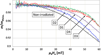
Figure 8. Normalized magnetization curves as a function of external applied field for all investigated samples.
Download figure:
Standard image High-resolution imageThe magnetic hysteresis loops were measured in order to analyse the effect of laser irradiation on the bulk pinning behaviour and the critical current density. Wider magnetization loop in general indicates stronger bulk pinning and higher pinning-based critical current density. The ability of the material to trap the vortices depends on the type and density of material defects suitable to pin the vortices (pinning centres), such as grain boundaries, vacancies, dislocations or precipitates. The curves in the figure 9 show that the width of the magnetization loops increased in all four cases after laser irradiation. This is consistent with the fact that laser irradiation caused finer crystalline structure of the Nb, creating more pinning centres in the film volume. Similar effect was observed in the study [21] after laser irradiation of the Nb film.
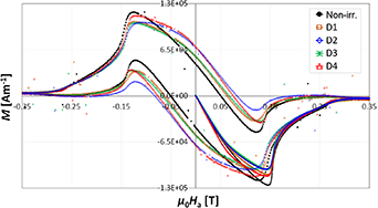
Figure 9. DC magnetic hysteresis loops for all of the investigated samples.
Download figure:
Standard image High-resolution imageGraphs in figure 10 show comparison between surface roughness Ra, lattice parameter a, L-vol parameter, crystalline size and Hen in dependence of the laser dose D. The first flux entry field Hen shows good correlation with the surface roughness Ra, which is associated with the surface features observed by the SEM analysis. The sample irradiated by the dose D4 shows relative increase of Hen by 51%. It is characterized by a smoother surface with some of initial corrugation still persisting and by disappearance of the pits. The highest relative increase by 65% was achieved in the sample irradiated by the dose D3, which has smoother surface compared to the D4 sample and no occurrence of the pitting. A considerably lower relative increase in Hen of 23% and 27% was obtained for the samples irradiated by laser doses D2 and D1, respectively. These samples look well smoothed without any of the initial corrugation persisting, but the holes emerged on their surfaces.

Figure 10. Correlation between: (a) surface roughness Ra and Hen as a functions of laser dose D (non-irradiated sample is plotted as zero laser dose), (b) lattice parameter a and Hen vs D, (c) L-vol and Hen vs D, and (d) crystalline size and Hen vs D.
Download figure:
Standard image High-resolution image
As these DC measurements are very surface-sensitive, the increase in Hen after laser irradiation was not surprising due to observed smoother surfaces and reduced surface defects. The results show that the first flux entry field was mostly influenced by the localized enhanced magnetic field created by the many sources such as grain boundaries [46], pits [47], micro-particles [3], microscopic surface roughness [16] or crystalline defects [17]. As the laser irradiation led to compactness/uniformity of the grains at the surfaces (figure 4), the enhancement of the localized magnetic field at a grain boundaries became lowered [46]. Disappearance of the initial corrugation reduced the enhanced magnetic field as well. However, the presence of the pits or holes have a much bigger effect on enhancement of the magnetic field, as analytically studied in [47]. This mechanism was reduced at the samples irradiated by laser doses >175 J cm−2 which exhibited the holes on the surfaces resulting in lowered increase in Hen. Improvement of the surface morphology after laser irradiation which led to reduced surface roughness has indeed good correlation with a change of Hen as we observed. The maximum increase in Hen thus seems to be associated with the dose showing the maximum improvement of the surface morphology without further defect formation. From the limited number of different laser energy doses we were able to apply, the dose D3 shows the best results in terms of the Hen improvement.
Moreover, the temperature generated by the laser is able to vaporize nearly any contaminant material presented on the Nb surfaces which could also have some contribution in the final SC properties [24]. The laser irradiation also caused a minor increase in lattice parameters as shown in the figure 10(b). However, the increase is not significant (∼0.08% at maximum between non-irradiated sample and D4) and there is probably only negligible impact on Hen change. Figures 7(c) and (d) show that the laser irradiation of Nb surfaces led to reduction of crystallite size as a consequence of rapid solidification of the melted Nb.
It needs to be mentioned that the maximum temperature generated by the laser was distributed close to the Nb surface and rapidly decreased with a distance [22] and thus it can be expected that the properties of the Nb will be different at every stage of the Nb thickness. The effect of laser annealing on DC superconducting properties is then a result of Nb properties through its whole volume. Using a measurement technique [26–31] which applies external magnetic field only from the side of Nb surface would eliminate this problem and it would provide results closer to real SRF applications. All the results presented in this work demonstrate that properties of a superconducting Nb thin film, in particular the first flux entry field, can be enhanced by the laser treatment. Further investigation will include more produced samples which will be characterized varying the film deposition parameters, the film thickness and the laser parameters. Laser treatment should be applied to larger surface area. Such samples will open the possibility of measuring their properties by means of magnetic field penetration method [29], AC/DC magnetic field analysis with 3rd harmonics [27, 28] and at the RF conditions with a quadrupole resonator [48]. Finally, to see an applicable effect of laser treatment, it should be adopted to treat a curved surface of an RF cavity.
4. Conclusions
The effect of Nd:YAG laser post-treatment of the Nb film deposited on Cu substrate (polished by EP+SUBU5) was studied in dependence on different energy dose applied (D1 = 350, D2 = 233, D3 = 175 and D4 = 140 J cm−2). The superconducting properties with main emphasis on first flux entry field Hen and characteristics obtained by AFM, SEM and XRD were compared before and after laser irradiation.
Compared with the non-irradiated sample, the Hen increased gradually with laser dose used up to the point where the new defects (holes) appeared on the Nb surfaces. Certain correlation between reduced surface roughness and enhanced Hen has been observed. Our study has shown that the laser treatment of the Nb film is able to increase the Hen even though new defects appeared in some cases. The best outcome was a 65% increase of Hen for the sample irradiated by the dose D3. The results show that Nb film morphology and structure as well as the superconducting and microstructural properties of the thin Nb films can be enhanced by laser treatment.
Acknowledgments
This research has been supported by European Commission's ARIES collaboration H2020 Research and Innovation Programme under Grant Agreement No. 730871 and by the VEGA Grant Agency under the contract VEGA 2/0097/18. The authors would like to acknowledge A Sublet for providing the copper substrates, C Z Antoine, M Vogel, S Leith and O Kugeler for several fruitful discussions and the whole team of the ARIES-Workpackage 15 for their help and technical support.
Data availability statement
The data that support the findings of this study are openly available at the following URL/DOI: DOI: 10.1016/j.apsusc.2020.146528.