

Abstract
Since 2009, metal halide perovskites have attracted a great deal of attention in different optoelectronic applications, such as solar cells, photodetectors (PDs), light-emitting diodes, lasers etc, owing to their excellent electrical and optoelectrical properties. However, since the discovery of graphene, atomically thin 2D materials have been the central focus of materials research due to its exciting properties. Thus, integrating 2D materials with perovskite material can be highly promising for various optoelectronic applications, in particular for ultrasensitive photodetection. In these PDs, 2D materials serve various roles, such as charge transport layer, Schottky contacts, photo absorbers, etc, while perovskite is the light-harvesting active layer. In this review, we focus on the recent findings and progress on metal halide perovskite/2D material phototransistors and hybrid PDs. We comprehensively summarize recent efforts and developments of perovskite/graphene, perovskite/transition-metal dichalcogenides, perovskite/black phosphorus, and perovskite/MXene based phototransistor and heterojunction PDs from the perspective of materials science and device physics. The perovskite/2D material phototransistor can exhibit very high photoresponsivity and gain due to the amplification function of transistors and the pronounced photogating effect in 2D material, while perovskite/2D material heterojunction PD can operate without external bias due to built-in potential across the heterojunction. This review also provides state-of-the-art progress on flexible, transparent, self-powered and PD systems and arrays based on perovskite/2D materials. After summarizing the ongoing research and challenges, the future outlook is presented for developing metal halide perovskite/2D material hybrid PDs for practical applications.
Export citation and abstract BibTeX RIS

Original content from this work may be used under the terms of the Creative Commons Attribution 4.0 license. Any further distribution of this work must maintain attribution to the author(s) and the title of the work, journal citation and DOI.
1. Introduction
Photodetectors (PDs) are representative optoelectronic devices that can convert optical signals into electrical ones based on the photoelectric effect, which are one of the key components in contemporary multifunctional technologies [1–7]. The efficient and ultrasensitive photodetection is very important in a wide range of fields, such as optical communication, spectroscopy, biomedical imaging, environmental monitoring, biological/chemical sensing, security, fire detection, night vision, motion detection, video imaging, etc [1–6, 8]. In the high-performance PD, typically semiconducting materials are used which efficiently absorb incident photons and produce electron–hole pairs upon photoexcitation, and built-in electric field or external bias is used to separate photogenerated carriers effectively to generate an electrical output [1–6, 9, 10]. Currently, the PDs in the entire UV–NIR spectrum are dominated by detectors fabricated from inorganic semiconductors, such as GaN, Si, and InGaAs [8, 11]. Typically, GaN operates in the UV region, while Si and InGaAs respond in Vis–NIR and NIR–far NIR region, respectively. However, there are certain limitations and shortcomings in these PDs due to their complicated manufacturing technologies, high-quality crystals with low defects, high power consumption, high cost and bulkiness of the devices. Therefore, low-cost PDs with broadband light detection, high sensitivity and fast response are highly desirable. Low-cost and solution-processable optoelectronic materials, such as organic semiconductors, different semiconductor nanostructures have been explored for efficient photodetection. However, the performance of these PDs is often restricted due to their poor charge–carrier mobility. Interestingly, halide perovskite-based semiconductors have shown great promises in low-cost PDs. We provide below a brief account of the important properties of perovskite and 2D materials that are most relevant for PD applications.
1.1. Fundamentals of photodetectors
A PD generally converts the incident optical signal into charge–carrier flux. A PD can work based on two mechanisms: (a) an external field-assisted transport of photoexcited carriers in which the applied external field can stimulate a large number of carrier transport by detrapping of trapped photogenerated carriers; (b) the photogenerated charge carriers produce an electric field, which decreases the injection barrier and consequently amplifies the charge injection. The diffusion and drift of photogenerated charge carriers, the recombination dynamics, and the role of contacts need to be fully understood for the design and optimization of the device for a good PD [12]. Typically, there are two types of architectures for PDs: (a) lateral structure device and (b) vertical structure device [13, 14]. In a lateral structure device, active materials are directly connected to lateral electrodes, while the vertical structure device consists of different stacking layers. Lateral structure-based PDs include photoconductors and phototransistors, while vertical structure PDs include photodiodes, heterojunction PDs, solar cell structure (p-i-n or n-i-p) devices. Except for phototransistors, all the other PDs are two-terminal devices; one electrode is the cathode, and another is the anode. In contrast, phototransistors are PDs with three-terminal: gate, source, and drain electrodes [15, 16]. Figure 1(a) depicts a simple schematic of vertical structure PD while figure 1(b) shows a schematic illustration of PD with a lateral structure.
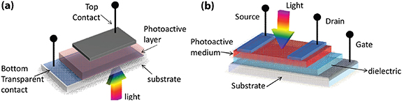
Figure 1. (a) Schematic illustration of the device configurations of (a) vertical structure and (b) lateral structure PDs. [14] John Wiley & Sons. [© 2013 WILEY‐VCH Verlag GmbH & Co. KGaA, Weinheim].
Download figure:
Standard image High-resolution imageThe photoconductor is a simple lateral system with two electrodes and light-absorbing direct bandgap semiconductors in between the electrodes. In this type of PDs, an external bias is applied to observe the light-induced change in conductivity. These PDs can exhibit high gain through multiple carrier recirculation. The metal-semiconductor Schottky junction also plays an important role in photodetection. The Schottky photodiode can operate in different modes: (a) photoexcitation and carrier generation in semiconductors, (b) generation of the carrier from metal to semiconductor over the Schottky barrier. The Schottky PDs can be very useful for broadband photodetection.
Photo field-effect transistors (photo FETs) comprise of a photoconductive channel with drain and source electrodes on two sides, and the carrier transport of the channel can be controlled by the applied gate bias. However, incident light produces photocarriers and serves as an additional gate. Thus, the electrical gate can be either open-circuited or externally biased to control the photoresponse characteristics of the device. In photo FETs, the channel materials should simultaneously exhibit both high carrier mobility and superior light-harvesting capability for efficient charge generation [17]. Note that 2D material shows superior mobility for carrier transport, whereas perovskites have excellent photoelectric conversion efficiency with high absorption coefficient. Thus, the perovskite/2D material hybrid system is a very promising channel material for photo FET. Under illumination, electron and hole pairs are generated in the perovskite layer, which further transports to the source and drain electrodes via the 2D material layer. The applied gate voltage can effectively increase the separation of photocarriers. In a photo FET, often one type of carrier is intentionally immobilized in the device, while another type is free to move and contribute to photocurrent by suitable choice of the materials and designs in the device [18]. This phenomenon is known as photogating effect. Due to the inherent amplification in FET, phototransistor can have high external quantum efficiency (EQE) exceeding 100%, high gain, and high responsivity, which can be controllable by gate bias. Though photo FET exhibits high responsivity, the response speed is significantly lower due to the trapped carriers.
Photodiodes are vertical structure devices in which the active layers are sandwiched between electrodes. Photodiodes may be p–n junction type or semiconductor heterojunction (like type-II) type. Photodiodes possess a very low dark current and very high detectivity of light due to interface layers. Due to the built-in potential, the photodiodes can also detect light without applied bias. These devices are known as self-powered PDs, which are very attractive from the application perspective. In the reverse-bias condition, photodiodes show superior performance due to an increase in charge collection efficiency. Besides, the response speed of photodiodes is generally higher compared to the other kinds of PDs.
Perovskite PDs with 'solar cell structure' (p-i-n or n-i-p) show excellent photodetection without any applied bias due to the photovoltaic effect. In this type of vertical structure device, perovskite serves as light-absorbing intrinsic (i) active layer and one-hole transporting layer (HTL) (p) and another electron transporting layer (ETL) (n) are used to separate and transport of photogenerated electrons and holes to the electrodes. However, as this involves the deposition of additional layers, it is not very commonly used.
To quantitatively measure the performance of a PD, there is a series of figures of merit, such as photoresponsivity (R), gain, specific detectivity (D*), EQE, linear dynamic range (LDR) and response speed, etc. The photoresponsivity of a PD indicates how efficiently the detector responds to an incident optical signal. The responsivity of a PD is a very important figure of merit that describes incident photon to the electrical signal conversion efficiency of the given PD. Responsivity is defined as the ratio of photocurrent to the power of incident light on the active area of PD by the following equation,

where  is the photocurrent defined as the difference between the current of the device in the presence of illumination and dark condition (
 −
−  ).
).  is the incident optical power on the active area of the PDs. Responsivity is generally proportional to the EQE for a PD. It is very significant for a good PD to have a high conversion rate from photons to electron–hole pairs.
The photoconductive gain (G) is defined as the number of charge carriers circulating through an external circuit per incident photon. It can be expressed as

where  represents the energy of the incident photons. By increasing the photoconductive gain of a PD, the sensitivity of the PD is also increased, which further makes it suitable for different applications, such as receivers in optical fiber communications, single-photon counting, laser microscopy, high-resolution imaging, etc [19]. The gain can also be obtained by measuring transit time and carrier-recombination lifetime as expressed by the given equation:

where d is the device thickness, μ is the carrier mobility and V is the applied bias.
The specific detectivity (D*) of a PD signifies the capability of detecting low-level light signals, taking into account the influences of the photocurrent and dark current. D* can be calculated by the equation:
where R is the spectral responsivity, q is the elementary electron charge and Jd (Jd = Idark/area of the device) is the dark current density of the device. Note that this equation is valid only under the approximation that the dark current of the PD is dominated by the shot noise. The high detectivity of a PD represents that the PD can detect very low-intensity light signals. The specific detectivity of a PD can also be expressed by noise-equivalent power and the electrical bandwidth of device noise:
where NEP represents the noise equivalent power, A is the working area of the PD and B is the bandwidth. The NEP of a PD is defined as the signal power that gives a signal-to-noise ratio of one. For a sensitive PD, NEP should be small.
A good PD should detect incident light with an identical responsivity over a wide range of light intensity. This characteristic of the PD is defined as the LDR. LDR can be expressed as

where Jph and Jd are the photocurrent and dark current densities of the device, respectively. In the LDR limit, a PD can detect light precisely.
One of the critical parameters of a PD is response speed. The response speed of a PD is calculated from the rise and fall times of a transient photocurrent. The photocurrent growth and decay times can be defined as the times taken for a photocurrent to reach 63.2% and to drop to 36.8% of the steady-state values, respectively. For pulsed illumination cases, the rise and fall times are the time intervals between photocurrent level reaching ∼10% and ∼90% of its saturation level upon on/off illumination cycles. The rise and fall time constants can also be calculated from the curve fitting of the temporal photoresponse by the exponential function [20].
1.2. Properties of perovskites for photodetection
Over the past one decade, halide perovskite materials with structural formula ABX3 (where A and B are cation and X is halide anion) have emerged as a promising class of semiconductors, which are being studied extensively for their applications in different optoelectronic devices, such as, solar cells, light-emitting diode (LED), PD, laser etc [2, 11, 21–37]. A tremendous research attention have been drawn for the investigation of high-performance hybrid perovskite-based optoelectronic devices due to its unique optical and electronic properties, such as high optical absorption coefficient, high carrier mobility, tunable optical band gap, long electron–hole diffusion lengths, and low-cost and low-temperature processing [2, 13, 21, 38–40]. Recently, the power conversion efficiency (PCE) of perovskite-based solar cells has achieved >23% [26, 41–43]. Thus, this new family of semiconducting optoelectronic materials with good solution-processability and low-cost fabrication can be a good alternative of well-established crystalline Si and group III–V semiconductors. Solution-processed low-cost metal halide perovskites have direct-bandgap with large absorption coefficients in the UV–visible range as compared to that of its low value in Si. For example, at 600 nm, the absorption coefficient of CH3NH3PbI3 perovskite is ∼105 cm−1, while that of Si is ∼104 cm−1 [44]. Due to the high absorption coefficient, a very thin layer of perovskite is adequate for almost complete light absorption in optoelectronic devices. Recently, low-cost perovskite PDs have been revealed to high responsivity and fast photoresponse, which makes them promising candidates for different light-detection devices [13, 45–58]. The responsivity (R) and detectivity (D*) of perovskite PDs have achieved over 109 A W−1 and 1016Jones, respectively, while the response speed is <1 ns, which are significant compared to other PDs [13, 48]. However, the application of perovskites in optoelectronic devices is limited due to the poor air-stability and toxicity of lead-based perovskite [42, 59]. The most of the reported high-performance perovskite PDs with high responsivity and ultrafast response time are planar or mesoporous 'perovskite solar cell structure'. Perovskite solar cells are photovoltaic devices with vertical architecture, which consists of different stacked layers. It generally comprises of (a) transparent conducting oxide electrode, (b) electron transporting material (ETM), (c) light-harvesting perovskite active layer, (d) hole transporting material (HTM), (e) counter electrode. In these types of p-i-n or n-i-p PDs, typically one electron transporting material and another hole transporting material are used to separate and transport photogenerated electrons and holes, while the perovskite layer acts as a light-absorbing active material. Dou et al have reported a vertical architecture of perovskite PD, similar to a solar cell configuration of ITO/PEDOT:PSS/CH3NH3PbI3−x Clx /PCBM/PFN/Al [60]. This PD showed a broad photoresponse in the wavelength region from 300 to 800, while the reported detectivity was observed to be 1014Jones, which is nearly one order of magnitude higher than the detectivity of a commercial Si-based PD. Bao et al presented a highly flexible self-powered perovskite PDs with the configuration of PEN/Au nanowire/CH3NH3PbI3/PCBM/Al with responsivity 321 mA W−1 and response speed of 4 μs [61]. Sutherland et al demonstrated a self-powered perovskite PD with the structure of FTO/TiO2/Al2O3/PCBM/CH3NH3PbI3/spiro OMeTAD/Au by exploiting interface engineering of the device with the response speed of 1 μs and responsivity of 0.4 A W−1 [62]. Zhang et al reported perovskite PDs with a controllable photoconductive gain by designing a trapped-electron-induced hole injection structure of ITO/PEDOT:PSS/CH3NH3PbI3/PCBM:F4-TCNQ/BCP/Au [63]. Interestingly, these PDs with solar cell architecture can operate without any external bias. The high performance of the perovskite PDs was attributed to the outstanding intrinsic optical and electronic properties of the solution-processed hybrid perovskites, as well as judicious device configuration and interface engineering.
1.3. Properties of 2D materials for photodetection
Since the discovery of graphene, 2D materials have attracted extensive attention due to their unique structures and their mechanical and physical properties [64–68]. The large family of 2D materials is mainly composed of the 2D atomic layer with the same elements, such as graphene and black phosphorus (BP), transition-metal dichalcogenides (TMDs), chalcogenides, oxides, nitrides, thiophosphates, halides etc [65, 69]. Due to the unique structure and novel properties, these 2D layered materials are very promising in various applications, such as solar cells, PDs, LEDs, biosensors, and so on [3, 66, 70–72]. Monolayer and few-layer 2D materials have been extensively applied in PDs, which shows very fast photoresponse speed along with high photoresponsivity due to the high carrier mobility, unique optical properties, and superior mechanical flexibility [70, 73–75].
However, the performance of these 2D material-based PD is usually limited by the low light-harvesting capacity of the monolayer and few-layer material. On the other hand, halide perovskite has an excellent capability of light-harvesting with a large absorption coefficient. Thus, the integration of 2D TMD materials with high light-harvesting perovskite materials can lead to substantial enhancement in the light absorption resulting in high photoresponsivity and fast response due to high carrier mobility in atomically thin 2D TMDs.
In this review, we present state-of-the-art progress in the PDs based on halide perovskite/2D material hybrids. First, we discuss the fundamental operational principles, device architectures, and different figures of merit of PDs. Next, we discuss on advances in perovskite/graphene based heterostructure PDs followed by a state-of-the-art account of the progress in TMDs/perovskite based heterostructure PDs. In particular, we discuss the advances in the perovskite/MoS2, perovskite/WS2, and perovskite/other TMDs (such as MoSe2, WSe2, PtSe2, PdSe2) based PDs. Next, we discuss about perovskite/BP-based PDs and perovskite/MXene based PDs, which are more recent additions to the family of 2D materials and are under development. Finally, we summarize the challenges and opportunities in the field followed by the future outlook for developing metal halide perovskite/2D material hybrid PDs for practical applications.
2. Perovskite/2D material photodetector
2.1. Perovskite/graphene photodetector
Graphene is a very interesting 2D material for optoelectronic applications [76, 77]. The concentrations of electrons and holes in the graphene layer exceed 1013 cm−2, while the carrier mobility is higher than 15 000 cm2 V−1 s−1 [78]. Because of its zero bandgap, graphene exhibits an extremely broadband absorption from UV to THz region. Most of the graphene-based PDs are constructed with a metal–graphene Schottky junction, a homogeneous p–n junction, or a tunneling barrier junction. The metal–graphene–metal Schottky junction PDs can operate by taking advantage of the work-function difference between a contact metal and graphene, which shows a very ultrafast photoresponse [79]. Xia et al demonstrated ultrafast phototransistor with monolayer and few-layer graphene with a 40 GHz bandwidth and a 0.5 mA W−1 photoresponsivity [80]. Mueller et al reported metal–graphene–metal PD with maximum external photoresponsivity of 6.1 mA W−1 by using two different metal electrodes [81]. The asymmetric metallization scheme results in a break of the mirror symmetry of the internal electric-field profile in conventional graphene FET channels, enabling an efficient photodetection. In the back gated graphene FET, the photocurrent is generated due to the illumination of metal/graphene interfaces, and the field arises from the charge transfer from the metal electrode to graphene. For the controllable p- or n-type doping in graphene, mostly surface chemical modification methods have been adopted. Liu et al reported a large area and flexible p–n junction graphene PD with good photoresponsivity in the infrared (IR) region [82]. The p–n junction in the graphene layer was fabricated by selected-area chemical doping in the chemical vapor deposition (CVD) process [82, 83]. Liu et al reported an ultra-broadband phototransistor consisting of a pair of stacked graphene monolayers separated by a thin tunnel barrier [84]. In the presence of light, hot carriers are generated in the top layer of graphene and further tunnel into the bottom layer, which leads to a charge build-up on the gate and a strong photogating effect occurs on the channel conductance. This PD could operate in the visible to the mid-infrared range, with mid-infrared responsivity higher than 1 A W−1.
The fundamental shortcomings of pure graphene-based PDs are its zero bandgap and poor absorbance of the incident light. Single-layer graphene can absorb only 2% of incident light over a broad wavelength region [84]. Due to the high conductivity, the dark current is also very high in pure graphene-based PDs. Thus, the integration of additional high light-harvesting materials, such as halide perovskite, can lead to substantial enhancement in the light absorption resulting in high photoresponsivity along with fast response due to high carrier mobility in graphene.
In 2015, Lee et al first reported a novel hybrid photo FET consisting of graphene and CH3NH3PbI3 perovskite layers [85]. CH3NH3PbI3 perovskite/graphene hybrid PD was fabricated on a SiO2/Si substrate (figure 2(a)). A heavily n-doped Si wafer served as a gate electrode, while 300 nm thick SiO2 layer was employed as the dielectric layer for the photo FET. Au electrodes deposited by thermal evaporation performed as source and drain electrodes. Further, CVD-grown single-layer graphene was transformed and pattern by photolithography. Finally, the CH3NH3PbI3 perovskite layer was deposited by spin coating of perovskite precursor onto the graphene surface. The UV–visible–IR absorption spectra of the perovskite–graphene hybrid system and pristine perovskite layer are shown in figure 2(b). The perovskite layer shows broad absorbance over the UV–visible–NIR region, which is essential for the broadband photodetection, and the absorption of the hybrid system was nearly unaltered in the presence of single-layer graphene. Interestingly, the photoluminescence (PL) intensity of the perovskite–graphene hybrid film was quenched by ∼65% compared to the pristine perovskite film (figure 2(c)), which was attributed to the effective transfer of photogenerated carriers through π–π interaction between perovskite and sp2 hybridized graphene layer. The incident wavelength-dependent photoresponsivity and EQE of the hybrid device match well with the absorbance of perovskite, i.e. the responsivity increases in the wavelength region <780 nm (figure 2(d)). The detection limit of the PD was 400–850 nm, which matches well with the absorbance of the composite film. Thus, the photocurrent was generated mainly due to the photoexcitation of the active perovskite layer. The variation of photoresponsivity and EQE as a function of the illumination power for the perovskite/graphene hybrid system is shown in figure 2(e). The inset of figure 2(e) shows the variation of detectivity of the hybrid PD. The hybrid PD showed a photoresponsivity of 180 A W−1 and an EQE of ∼5 × 10⁴% for an optical power in the microwatt range, while it decreases with the increase in intensity of the incident light. Note that the decrease in responsivity with increasing incident power is attributed to a higher probability of scattering and recombination under stronger illumination. The device exhibited good photoswitching behavior under the illumination of 520 nm with 0.5 mW incident power with gate (Vg) and drain voltages (Vds) of 0 and 0.1 V, respectively (see figure 2(f)). The upper portion of figure 2(f) shows the pulsed laser illumination response, while the bottom one is the temporal response of the photocurrent. The photocurrent growth and decay time constants were observed to be 87 and 540 ms, respectively. Thus, this work demonstrated a hybrid PD consisting of graphene and CH3NH3PbI3 perovskite layers with a broad spectral response and high EQE due to increased optical absorption and photogating mechanisms of the hybrid system. However, photoresponsivity of the reported device was relatively low compared to the other reported photo FETs based on perovskite/graphene which may be due to the defects and poorer morphology of perovskite active layer.
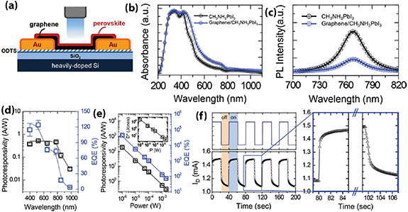
Figure 2. (a) Schematic illustration of the perovskite/graphene hybrid PD. (b) UV–Vis absorption spectra of the pristine perovskite and perovskite/graphene hybrid films. (c) Comparison of PL spectra of CH3NH3PbI3 film and CH3NH3PbI3–graphene hybrid films upon excitation at 532 nm. (d) Incident wavelength-dependent photoresponsivity and EQE of the hybrid PD. (e) Variation of photoresponsivity and EQE with the power of incident light. Inset shows the variation of detectivity with the power of incident light. (f) Temporal photocurrent response of the hybrid PD under alternating dark and light illumination (0.5 mW, 520 nm) with gate and drain voltages 0 and 0.1 V, respectively. The right panel shows an enlarged view of the photocurrent response during the on–off of the incident light. [85] John Wiley & Sons. [© 2014 WILEY‐VCH Verlag GmbH & Co. KGaA, Weinheim].
Download figure:
Standard image High-resolution imageWang et al reported a hybrid PD with an exceptionally high photoconductive gain of ∼109 electrons per photon and responsivity of ∼6.0 × 05 A W−1 that consists of monolayer graphene covered with a thin layer of dispersive CH3NH3PbBr2I halide perovskite islands [86]. The perovskite–graphene hybrid material was the photoactive channel material in phototransistor (figure 3(a)). CVD-grown graphene was transferred on Si/SiO2 substrate by wet transfer method, while perovskite precursor solution was deposited on top of the graphene layer by antisolvent assisted spin coating method to form perovskite islands. The transfer characteristics of the bare graphene transistor in dark condition show a charge-neutral point at ∼40 V, which is attributed to the p-doping effect caused by the SiO2 substrate and water trapped beneath the graphene film (figure 3(b)). In the case of graphene/CH3NH3PbBr2I perovskite island hybrid phototransistor, the charge neutral point was shifted to lower gate voltage, which was attributed to the decrease in p-doping effect in graphene due to electron transfer from perovskite. Due to the work function mismatch between these two materials, electrons were transferred from perovskite to graphene and a built-in electric field was developed, which led to band bending in perovskite to enable effective detrapping of photocarriers, as illustrated in the inset of figure 3(b). The temporal response of the photocurrent of the hybrid PD under the illumination of 405 nm light with power 921.5 nW shows good photo-switching behavior (figure 3(c)). The detection range of the PD was in the range of 250–700 nm, which matches with the absorbance of the perovskite active layer. The growth and decay times for photocurrent of perovskite–graphene island phototransistor were measured to be less than 120 and 750 ms, respectively (figure 3(d)). The variation of responsivity with drain–source (Vds) voltage at zero gate voltage is shown in figure 3(e). The responsivity was observed to be 6.0 × 10⁵ A W−1 under the illumination of 405 nm with a power of 1.052 nW and Vds of 3 V. The photocurrent was increased linearly with the increase of incident light power at relatively low power and eventually gets saturated at high power due to the increased recombination rate of photoexcited carriers (figure 3(f)). The photoresponsivity decreases with the increase in light power (figure 3(f)). Thus, the high performance of CH3NH3PbBr2I perovskite islands/graphene phototransistor is attributed to the effective charge transfer and photogating effect. Compared to the bulk perovskite thin-film case, the perovskite islands have a low bulk recombination rate of photogenerated carriers, which results in the enhanced performance of the PD [85, 86].
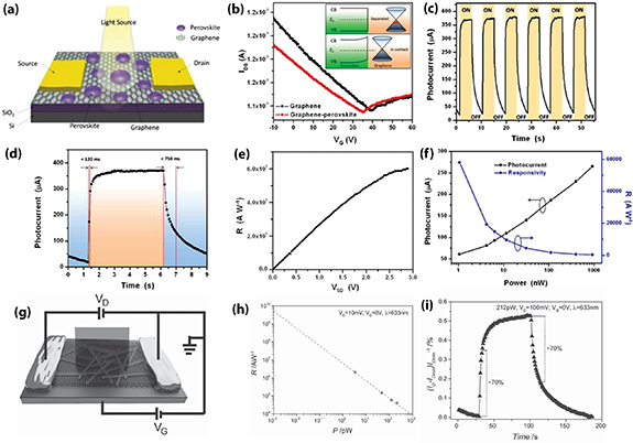
Figure 3. (a) Schematic configuration of CH3NH3PbBr2I perovskite island/graphene phototransistor. (b) Transfer characteristics of the devices based on graphene and graphene–perovskite hybrid. Inset shows the energy diagrams of graphene before and after being in contact with CH3NH3PbBr2I perovskite. (c) Temporal photocurrent response of graphene–perovskite island PD under the illumination of 405 nm laser of power 762.3 nW. (d) The response speed of the hybrid phototransistor. (e) Variation of photoresponsivity with the source–drain voltage at zero gate voltage. (f) Variation of photocurrent and responsivity with incident power for graphene–CH3NH3PbBr2I perovskite island hybrid. [86] John Wiley & Sons. [© 2015 WILEY‐VCH Verlag GmbH & Co. KGaA, Weinheim]. (g) Schematic representation of CH3NH3PbI3 nanowire/graphene phototransistor. (h) Variation of responsivity with an incident light power of CH3NH3PbI3 nanowire/graphene hybrid PD. (i) Photoresponse speed of the CH3NH3PbI3 nanowire/graphene hybrid phototransistor. [87] John Wiley & Sons. [© 2015 WILEY‐VCH Verlag GmbH & Co. KGaA, Weinheim].
Download figure:
Standard image High-resolution imageFurther, Spina et al reported CH3NH3PbI3 nanowire/graphene phototransistor, which shows photoresponsivity of 2.6 × 10⁶ A W−1 [87]. CH3NH3PbI3 nanowire was fabricated by the slip-coating method on top of single-layer graphene FET (figure 3(g)). The variation of responsivity of the PD with incident light intensity is shown in figure 3(h). The rise and fall times of the hybrid CH3NH3PbI3 nanowire/graphene PD were observed to be 55 and 75 s, respectively (figure 3(i)), which are comparatively higher than the perovskite-film based PD. The photocurrent response times can be divided into two components (figure 3(i)). The slow component is attributed to the multiplicity of charge traps in the nanowire film that stems from different surface states. The high responsivity of CH3NH3PbI3 nanowire/graphene is attributed to the enhanced light-harvesting capacity of perovskite with nanowire morphology.
Plasmonic metal nanoparticles (NPs) play a vital role in boosting the performance of optoelectronic devices [88–90]. Under photon illumination, plasmonic NPs can give rise to localized surface plasmon resonance (LSPR), which prompts strong photon absorption and scattering. Thus, due to the plasmonic scattering and near-field enhancement induced excitation effects, the photon absorption of the surrounding material can be improved [91–93]. Plasmonic metal NPs also helps in better charge separation and transport. Sun et al demonstrated a CH3NH3PbI3/graphene/Au NP hybrid photo FET with enhanced performance [94]. The perovskite active layer was physically separated by the ultrathin graphene layer from the Au NPs film. Au-NPs with a diameter of ∼40 nm were synthesized by a well-known citrate reduction method and transferred on the Si/SiO2 substrates through a self-assembled monolayer (SAM) of 3-aminopropyltriethoxysilane (APTES). The SEM image of the Au-NP-coated Si/SiO2 substrate is shown in figure 4(a), which confirms dense and uniform coverage of Au NPs on the substrate. The absorption of Au NPs is shown in the inset of figure 4(a), which depicts a plasmonic absorption peak at ∼530 nm. The schematic illustration of the CH3NH3PbI3/graphene/Au NP hybrid phototransistor is shown in figure 4(b). On top of the Au-NP film-coated Si/SiO2 substrate, graphene was transferred, and then CH3NH3PbI3 perovskite film was deposited on top of it by spin coating of the perovskite precursor solution. As illustrated in figure 4(b), in the CH3NH3PbI3/graphene/Au NP hybrid device, due to the near-field enhancement of Au-NPs, most of the photogenerated carriers are produced near the interface between graphene and perovskite layer. The enhanced photogenerated carriers due to the LSPR effect of Au NPs results in the enhanced photocurrent of the hybrid device. The transfer characteristics of pristine (without Au NPs) and the hybrid PD (with Au NPs) at VDS = 0.1 V under the illumination of 532 nm for different intensities are shown in figures 4(d) and (e), respectively. The transfer characteristics confirm the p doping in graphene due to the transfer of photogenerated charge carriers from perovskite to graphene, and a slightly enhanced photocurrent was observed in the hybrid device. The light intensity-dependent responsivity and EQE of the pristine and hybrid PDs are shown in figure 4(f). The responsivity of the hybrid device was increased by ∼100% compared to the device without Au-NPs, as shown in figure 4(f). Interestingly, as the photogenerated carriers are mostly produced near perovskite–graphene interface (figure 4(c)) due to the LSPR effect of Au NPs, the recombination rate can be greatly reduced, which leads to a slower drop of responsivity with increasing light intensity in the hybrid device compared to the pristine one (figure 4(c)). However, the highest responsivity was observed to be only ∼2 × 10³ A W−1. The photoresponse speed of the pristine and hybrid PD is shown in figure 4(g). The photocurrent growth time increased in the hybrid device compared to the pristine device. Thus, the possible mechanisms for the enhanced performance of the hybrid device may be attributed to: (a) the increase in light-harvesting in CH3NH3PbI3 perovskite due to the near-field enhancement on the surface of Au-NP, (b) superior separation of excitons and the extraction of carriers due to Au-NPs, (c) trap of minority carriers or suppression of the carrier recombination in CH3NH3PbI3 by Au NPs, (d) generation of hot carriers in Au-NPs and transfer into graphene and thus increase the photocurrent.

Figure 4. (a) SEM image of Au NPs coated Si/SiO2 substrate. Inset shows the UV–Vis absorbance spectrum of Au NPs. (b) Schematic of device architecture of CH3NH3PbI3/graphene/Au NP hybrid phototransistor. (c) Schematic of photo-induced carrier generation, diffusion and transfer in the device (d) Transfer characteristics of CH3NH3PbI3/graphene device. (e) Transfer characteristics of CH3NH3PbI3/graphene/Au NP hybrid phototransistor. (f) Variation of responsivity and EQE with incident light intensity. (g) Response time of device with Au NPs and without Au NPs. Reproduced from [94] with permission of The Royal Society of Chemistry. (h) Schematic diagram of CH3NH3PbI3−x Clx perovskite/(P3HT)/graphene phototransistor. (i) Responsivity of the device as a function of the back-gate voltage under illumination of different intensities. (j) Temporal photoresponse of the phototransistors with perovskite layer thickness of ∼300 nm (top panel) and ∼40 nm (bottom panel) under light intensity of 14.15 nW cm−2 and at VG = −25 V, respectively. Reprinted with permission from [95]. Copyright (2017) American Chemical Society.
Download figure:
Standard image High-resolution imageAnother approach to improve the performance of perovskite/2D material hybrid PD is the incorporation of charge-transporting layers, which enhances the efficiency of photocarrier separation. Note that generally in perovskite solar cells, one ETL and another HTL are used, which separate and transport the photo-induced carriers. Xie and co-workers reported CH3NH3PbI3−x Clx perovskite/poly (3-hexylthiophene) (P3HT)/graphene multi-junction ultra-sensitive phototransistor [95]. The device configuration of CH3NH3PbI3−x Clx /P3HT/graphene multi-junction PD is shown in figure 4(h). In this multi-junction device, CH3NH3PbI3−x Clx mixed halide perovskite layer serves as a light-absorbing active material that absorbs light and generates electron and hole pairs, while P3HT acts as an HTL to efficiently separate electrons and holes reducing the carrier recombination. The graphene layer provides a fast charge transfer channel. The light intensity-dependent responsivity of CH3NH3PbI3−x Clx perovskite/P3HT/graphene phototransistor as a function of back–gate voltage, VG is shown in figure 4(i). The device exhibits a responsivity as high as ∼4.3 × 10⁹ A W−1 along with a photoconductive gain of ∼8.9 × 10⁹ at the excitation wavelength of 598 nm (figure 4(i)). The maximum responsivity of the device with P3HT HTL was increased by one order of magnitude compared to the device without the HTL layer due to the enhanced carrier separation by the HTL. The photoresponse speed of the phototransistors with a perovskite layer thickness of ∼300 nm (top panel) and ∼40 nm (bottom panel) under the illumination of intensity 14.15 nW cm−2 at VG = −25 V are shown in figure 4(j). Here, the device with a lower thickness of perovskite layer shows faster response due to the superior photogating effect. The PD showed good photoresponsivity in the wavelength range 400–800 nm. Note that the photoresponsivity of the device is significantly higher than the other reported perovskite/graphene PDs, which is attributed to the enhanced carrier separation by the HTL.
Qin and co-workers used [6,6]-phenyl-C61-butyric acid methyl ester (PCBM) electron transport layer in CH3NH3PbI3/graphene phototransistor for improved charge separation and transport [96]. They dissolved different amounts of PCBM (0%, 0.1%, and 1%) into the perovskite precursor solution and spin-coated it by a one-step antisolvent method on top of the graphene. After transforming into perovskite film, PCBM was observed near the grain boundaries of perovskite forming a bulk heterojunction (BHJ). Figure 5(a) shows the schematic architecture of BHJ–graphene PD. Under photon excitation, electrons and holes were generated in the perovskite. The electrons were captured by PCBM while holes were transferred effectively to the graphene layer resulting in the superior carrier separation (figure 5(a)). Thus, a net amount of negative charges build up in the BHJ layer, which induces hole doping in graphene and lowers the Fermi level (Ef). The charge transfer process and the electronic structure of the heterojunction are shown in figure 5(b). The photocurrent growth time was observed to be 2.5, 49, and 92 s for a device with 0%, 0.1% and 1% of PCBM, respectively. Thus, the longer photocurrent rise time found in the BHJ devices indicates that a longer time is required to attain the equilibrium carrier concentration within the active layer. This behavior is attributed to the de-trapping of electrons from PCBM, which is an extremely slow process that can last up to a few seconds. Similarly, the photocurrent decay times were found to be 65, 226, and 6203 s for the devices with 0%, 0.1%, and 1% of PCBM, respectively (figure 5(c)). The photo responsivities for the three devices as a function of incident illumination power are shown in figure 5(d). The responsivity of the pristine device was observed to be 3 × 10⁴ A W−1 for an incident power of 1.2 nW, while it increases to 1 × 10⁵A W−1 for the 0.1% PCBM device and 8 × 10⁵A W−1 for the 1% PCBM device under the same incident power. Thus, the responsivity of the device with 1% of PCBM was increased by a factor of ∼30 as compared to the device without the PCBM. Thus, a small amount of electron acceptor in the perovskite active material is responsible for the 30 fold enhancement of photo responsivity due to the superior carrier separation. Though the photo FET exhibited high responsivity, it showed very slow photoresponse speed compared to other perovskite/graphene photo FETs, which may be due to the trap states present at the interface of the device.
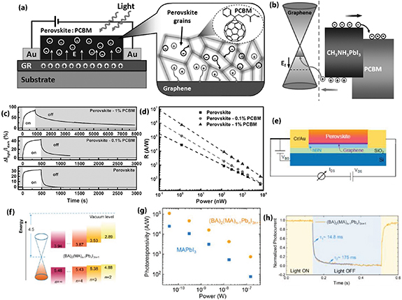
Figure 5. (a) A schematic diagram of the BHJ/graphene PD along with the electronic processes. (b) The energy band diagram of the PCBM–perovskite/graphene heterojunction. (c) Time-dependent photoresponses of devices with different PCBM concentrations under the light of wavelength 500 nm. (d) Responsivity of different devices as a function of incident light power. [96] John Wiley & Sons. [© 2017 WILEY‐VCH Verlag GmbH & Co. KGaA, Weinheim]. (e) Schematic device structure of hBN/graphene/(BA)2(MA)n –1Pbn I3n+1 2D perovskite phototransistor. (f) Comparative band energy diagram of the graphene/(BA)2(MA)n –1Pbn I3n+1 heterojunction with different n. (g) Responsivity of the device with 2D perovskite and conventional 3D CH3NH3PbI3 perovskite under different illumination intensities. (h) Time-dependent photocurrent response of the device with 2D perovskite. Reprinted with permission from [20]. Copyright (2017) American Chemical Society.
Download figure:
Standard image High-resolution imageDespite excellent optoelectronic performances, conventional 3D organometal halide perovskite materials start degrading upon exposure to water and oxygen molecule. These limitations may restrict the practical applications of conventional 3D perovskite/graphene-based PD. On the other hand, 2D organic–inorganic perovskites emerge as an alternative material for their 3D counterparts in optoelectronic applications with improved moisture resistance. Shao et al demonstrated hexagonal boron nitride (hBN)/graphene/2D multiphase perovskite PD (figure 5(e)) [20]. (BA)2(MA)n –1Pbn I3n+1 (where BA+ = CH3(CH2)3NH3 + and n is the number of lead iodide octahedral layers between two BA+ organic spacers). Depending upon integer n, the energy level diagram of the heterojunction is shown in figure 5(f). The photogenerated holes can be trapped effectively in 2D perovskite active layer while the electron can transfer easily to the graphene under layer. Due to the excellent carrier mobility of graphene on top of the ultra-smooth h-BN flake, the responsivity of the detector was observed to be ∼105 A W−1 (figure 5(g)) while the photoresponse time was found to be less than 200 ms (figure 5(h)). The photo FET exhibits a detectivity of 3.3 × 10¹⁰ Jones under incident light power of 42 pW. Interestingly, photo responsivity and the response time of the 2D perovskite/graphene phototransistor is much superior compared to the control CH3NH3PbI3/graphene device (figures 5(g) and (h)). The PD exhibits good responsivity in a broad wavelength range from 400 to 740 nm. 2D multiphase perovskite/graphene hybrid device also showed excellent ambient air stability compared to the conventional 3D perovskite.
Flexible PDs are highly desirable for different daily life applications. It can be attached to human skin for human–machine interfaces or combined into clothing to detect harmful light while being worn [97, 98]. Dang and coworkers fabricated CH3NH3PbI3/graphene hybrid phototransistor on a flexible substrate [99]. The photo FET consisted of a photoactive CH3NH3PbI3 perovskite and charge transporting graphene hybrid material that was a channel within the phototransistor. The hybrid channel was placed on top of the gate dielectric layer of Al2O3/polyvinylphenol/Al2O3 fabricated on the Ni gate electrode over the flexible polyimide substrates (figure 6(a)). Figure 6(b) shows the variation of responsivity of the flexible PD with incident light intensity. The maximum responsivity of the device was observed to be ∼115 A W−1, which is comparable to the first reported perovskite/graphene phototransistors on a rigid substrate [85]. The comparison of responsivity (figure 6(c)) and photoresponse time (figure 6(d)) up to 3000 bending cycle to a radius of 12 mm shows excellent performance of the device. No notable change in responsivity and response time was observed up to 3000 bending cycles suggesting robust bending durability of the flexible detector. Though the photoresponsivity of the device was relatively low, these results were significant for perovskite-based flexible PDs. Cheng and colleagues reported a barristor-type phototransistor based on graphene/CH3NH3PbI3 perovskite/graphene vertical heterostructure with maximum gain and responsivity of 2200 and 950 A W−1, respectively [100]. The photocurrent rise time and fall time were obtained to be 22 and 37 ms, respectively.
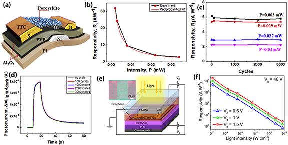
Figure 6. (a) Schematic architecture of CH3NH3PbI3/graphene flexible phototransistor. (b) Variation of the responsivity with an incident power of the flexible PD. (c) Responsivity of the flexible PD before and after cyclic bending up to 3000 cycles at a 12 mm bending radius. (d) Comparison of the response speed of the flexible PD up to 3000 bending cycles. Reprinted from [99], Copyright (2016), with permission from Elsevier. (e) Schematic illustration of the vapor-deposited perovskite–graphene hybrid phototransistor. (f) Variation of responsivity as a function of light intensity for the hybrid phototransistor at different drain voltages. Reproduced from [101]. CC BY 4.0.
Download figure:
Standard image High-resolution imageIn the above discussed PDs, solution-processable spin coating technique was used for the deposition of the perovskite active layer. Though these devices show excellent optoelectronic performances, reproducibility and large-scale perovskite deposition are the significant problems in spin coating and other solution-processable deposition techniques. Chang et al demonstrated a very smooth and compact perovskite film compared to the spin coating method by dual-source vapor deposition technique for graphene/perovskite hybrid phototransistor [101]. Graphene was transferred on a SAM-modified SiO2 substrates, which significantly improved the electrical properties of graphene (figure 6(e)). Finally, poly(methyl methacrylate) (PMMA) was spin–coated on the entire surface of the device for encapsulation from ambient moisture and oxygen (figure 6(e)). The maximum responsivity of the device was observed to be ∼1.73 × 10⁷ A W−1, while the photoconductive gain was ∼106 (figure 6(f)). The highest detectivity of the device was observed to be 2 × 10¹⁵Jones. The PD exhibited good photoresponsivity in the wavelength region of 450–700 nm. These results are significant for the development of large area perovskite/graphene PD with high photoresponsivity.
Bessonov et al reported a perovskite/graphene phototransistor based on a CH3NH3PbI3–PbS quantum dot (QD) absorbing layer, which shows a responsivity of ∼2 × 10⁵A W−1, a specific detectivity of 5 × 10¹² Jones, and a gain of >107 [102]. The photocurrent response time was observed to be ∼0.5–1 s. In their device, PbI2 and CH3NH3I co-mediated ligand exchange in PbS QDs enhances surface passivation and facilitates electronic transport, yielding faster charge recovery with larger gain [102].
Qian et al reported a solution-processed phototransistor utilizing perovskite-nitrogen-doped graphene QDs (NGQDs) composite film and a mildly reduced graphene oxide (mrGO) layer [103]. The device configuration of NGQDs-modified perovskite/mrGO phototransistor is illustrated in figure 7(a). GO sheets were spin-coated and bonded to the SiO2/Si substrate via a monolayer of APTES. Next, the GO film was mildly reduced by annealing at 150 °C for 30 min to increase its electrical conductivity. The NGQDs–CH3NH3PbI3 layer was spin-coated onto the mrGO layer. The device configuration is shown in figure 7(a). In this device, perovskite serves as light-absorbing active material, which produces photo-generated carriers, while mrGO acts as a charge transport layer. NGQDs serve as an electron acceptor in the device, which further optimizes the band alignment to facilitate photo-generated electron transfer from perovskite to mrGO. The band structure of the hybrid system is shown in figure 7(b). With the increase in light illumination intensity, the photocurrent increased gradually, while the responsivity and detectivity decreased (figure 7(c)). The responsivity of the PD was observed to be 1.92 × 10⁴ A W−1 at a gate voltage of 40 V and under light irradiance of 23.6 μW cm−2, while the corresponding specific detectivity (D*) was calculated to be 2.71 × 10¹³ Jones (figure 7(c)). The incident light wavelength-dependent responsivity and gain are shown in figure 7(d). It is evident that the hybrid phototransistor can detect photon in the entire UV–visible–NIR region due to the broadband optical absorbance by the CH3NH3PbI3 perovskite active layer. The photoconductive gain of the NGQDs–CH3NH3PbI3/mrGO phototransistor was measured to be as high as 1.0 × 10⁴ at 660 nm of the incident light (figure 7(d)). The photocurrent growth and decay times of the device were found to be 13 and 10 ms, respectively, at 660 nm (figure 7(e)). Thus, the hybrid photo FET exhibited faster photoresponse speed as compared to other reported perovskite/graphene based PDs. As perovskites possess poor ambient stability, the device was encapsulated with PMMA to improve the ambient stability. The PMMA encapsulated device maintained 85% of its initial photoresponsivity for as long as 20 d of storage in ambient air (figure 7(f)). Thus, this device showed excellent stability compared to other reported graphene/perovskite PDs.
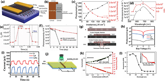
Figure 7. (a) Schematic illustration of the structure of NGQDs-CH3NH3PbI3/mrGO phototransistor. (b) Energy level diagrams of CH3NH3PbI3 perovskite, NGQDs, and mrGO heterojunction. (c) Variation of photocurrent and responsivity as a function of incident light intensity at 660 nm. (d) Wavelength-dependent responsivity and gain. (e) Temporal photocurrent response of the PD. (f) Stability of the device with and without PMMA encapsulation stored in ambient air. [103] John Wiley & Sons. [© 2017 WILEY‐VCH Verlag GmbH & Co. KGaA, Weinheim]. (g) The schematic of the Schottky junctions of the perovskite PD (P), the graphene/perovskite vertical structure device without channel (GP), and graphene/perovskite/graphene horizontal structure PD with one channel on the graphene (GPG). (h) I–V characteristics of the Schottky junction devices under illumination. (i) Time-dependent photocurrent response of the three devices. [104] John Wiley & Sons. [© 2019 WILEY‐VCH Verlag GmbH & Co. KGaA, Weinheim]. (j) Schematic illustration of CH3NH3Br3/N-rGO hybrid PD device with the gap between two ITO plates to be 40 μm. (k) Photocurrent and responsivity at different incident power under 4 V bias. (l) Wavelength-dependent responsivity of the device. Inset shows the absorbance of the active material. Reprinted with permission from [105]. Copyright (2020) American Chemical Society.
Download figure:
Standard image High-resolution imageThe above discussed all the graphene/perovskite PDs consist of FET type architecture. Chen and co-workers recently reported graphene/CH3NH3PbI3 perovskite/graphene (GPG) Schottky junction high-performance hybrid PD [104]. Graphene films of area ∼3 × 5 mm2 were synthesized on the copper foil through the CVD process and then transferred to the SiO2 (300 nm)/Si or flexible PET substrates. They fabricated three types of PD: (a) perovskite PD (P), (b) graphene/perovskite PD with vertical structure and without channel (GP), and (c) graphene/perovskite/graphene horizontal structure PD with one channel on the graphene (GPG). The schematic of the Schottky junctions of the three devices is shown in figure 7(g). A 20 μm wide channel on graphene converted the Schottky junction from vertical structure to vertical/horizontal hybrid structure in the GPG device (figure 7(g)). The GPG heterojunction device exhibits a very low dark current, which results in a high photoconductive gain. The I–V characteristics of the three devices are shown in figure 7(h), while the time-dependent photocurrents of the respective devices are shown in figure 7(i). The GPG detector showed a responsivity of 22 mA W−1 under the illumination of 452 nm light at 2.1 mW cm−2 with the corresponding photoconductive gain of 2.64 × 10³. Thus, the performance of the GPG Schottky junction PD was improved due to the low leakage current. They also demonstrated GPG PD on flexible PET substrate that showed robust bending durability.
Tang et al recently reported the spontaneous growth of CH3NH3PbBr3 perovskite/nitrogen-doped reduced graphene oxide (N-rGO) hybrid structures using a facile solution-processable method and their application for PDs [105]. CH3NH3PbBr3/N-rGO hybrid material was drop cast onto two neighboring ITO electrodes and fabricated PD, as illustrated in figure 7(j). The device shows the responsivity of as high as 3.6 × 10⁴ A W−1 and LDR of 94.4 dB at 4 V of applied bias (figure 7(k)). The detection range of the phototransistor was 365 to 940 nm. The variation of responsivity of the device with a wavelength of incident light is shown in figure 7(l), while the inset of the figure shows the absorption for the CH3NH3Br3/N-rGO hybrid. The photoresponsivity of the device matches well with the absorbance of active material. The EQE of the device was observed to be >105% and detectivity up to 1012 Jones were measured in the optimal device with the weight ratio between perovskites and N-rGO to be 16:3. The rise and decay times of the device were reported to be 30 and 100 ms, respectively. The superior performance of the CH3NH3PbBr3/N-rGO PDs is dominated by both intrinsic conductivity of the micro-crystals film and interfacial separation of photo-induced charge carriers. Chen and co-workers demonstrated all-inorganic CsPbBr3 perovskite/multilayer graphene structure for optical-fiber-compatible PD, which showed a responsivity of 2 × 10⁴ A W−1 [106].
Perovskite nanocrystals (NCs) and QDs show very interesting size-dependent optical and electronic properties that vary significantly from their bulk counterpart. Perovskite NCs and QDs also show excellent optoelectronic properties with the advantages of low-cost solution process synthesis, high PL quantum yield, higher photostability and widely tunable spectral range [107, 108]. Kwak et al reported hybrid CsPbBr3−x Ix NCs/graphene photo FET [109]. Figure 8(a) depicts the schematic device configuration of the hybrid CsPbBr3−x Ix NCs/graphene PD. The responsivity and detectivity of the hybrid device under 405 nm illumination with different optical power densities are shown in figure 8(b). This hybrid PD exhibits an impressive photoresponsivity of ∼108 A W−1 and detectivity of ∼1016 Jones under 405 nm illumination at 0.07 mW cm−2. The wavelength-dependent photocurrent (black dot) of the graphene–CsPbBr3−x Ix NCs PD and absorption spectra (blue line) of CsPbBr3−x Ix NCs are shown in figure 8(c). The spectral dependence of photocurrent of the device matches well with the absorption spectra of the active material exhibiting the photocurrent peak at 580 nm (figure 8(c)) and good photocurrent up to 600 nm. The photocurrent growth and decay times of the PD were found to be 0.81 and 3.65 s, respectively (figure 8(d)). Note that the reported photoresponsivity is the highest among the inorganic perovskite/graphene-based hybrid PDs, though the response speed is relatively slow.

Figure 8. (a) Schematic diagram of CsPbBr3−x Ix NCs/graphene PD. (b) Responsivity and detectivity of the PD at different incident powers for wavelength 405 nm and bias voltages of VDS = 1 and VGS = −60. (c) Comparison of the spectral dependence of the photocurrent and the absorbance of the perovskite active material. (d) Temporal photocurrent response of the device showing the response speed. Reproduced from [109] with permission of The Royal Society of Chemistry. (e) Schematic diagram of FAPbBr3 QDs/graphene hybrid PD. (f) Energy level diagram of FAPbBr3 QDs/graphene PD. (g) The photoresponsivity of the device as a function of incident illumination wavelength. (h) The photoresponsivity and EQE of the device as a function of light power of wavelength 520 nm and VDS of 2 V. [110] John Wiley & Sons. [© 2018 WILEY‐VCH Verlag GmbH & Co. KGaA, Weinheim]. (i) Schematic of the CsPbBrx I3−x perovskite NCs/graphene hybrid phototransistor. (j) Schematic illustration of the band bending in NCs and graphene before and after contact, and hole injection from NCs to graphene under illumination. (k) Variation of responsivity and detectivity of the hybrid device with incident light intensity. (l) Temporal photocurrent response of the PD. Reprinted with permission from [111]. Copyright (2019) American Chemical Society.
Download figure:
Standard image High-resolution imagePan et al demonstrated formamidinium lead bromide perovskite QDs (FAPbBr3)–graphene hybrid phototransistor [110]. The schematic diagram of hybrid graphene–FAPbBr3 QDs PD fabricated on SiO2/Si substrate is presented in figure 8(e). The built-in electric field of the perovskite/graphene interface helps in the separation of the photogenerated carriers (figure 8(f)). The photoexcited electrons in perovskite QDs are transferred to graphene, leaving holes trapped in the QDs due to the built-in electric field. The wavelength-dependent photoresponsivity of the PD at Vds = 2 V matches well with the absorption spectrum of the perovskite (figure 8(g)). A responsivity of 1.15 × 10⁵ A W−1 and EQE of 3.42 × 10⁷% of the PD were found under an illumination power of 3 μW at 520 nm wavelength (figure 8(h)). The PD exhibited a photoresponse speed of 60 ms at 538 nm of the incident light.
Surendran et al reported all-inorganic CsPbBrx I3−x perovskite NCs/graphene hybrid phototransistor where NCs serve as a photo absorber and graphene act as a transport layer [111]. The schematic of the device configuration is shown in figure 8(i). Figure 8(j) illustrates the energy band diagram of the hybrid PD before and after the graphene–perovskite contact and photogenerated hole injection and p doping in the graphene layer. The PD exhibits maximum of responsivity of 1.13 × 10⁴ and 7.12 × 10³ A W−1 at 80 μW cm−2 for gate bias voltages VGS = −60 V and +60 V, respectively, while the corresponding detectivity was found to be 1.17 × 10¹¹ Jones and 6.16 × 10¹⁰ Jones, respectively (figure 8(k)). The photocurrent growth and decay times of the phototransistor were found to be 273.6 ms and 2.26 s, respectively (figure 8(l)).
Cottam et al recently demonstrated a defect-assisted high photoconductive gain in graphene all-inorganic cesium lead halide perovskite NCs phototransistors [112]. The device shows stable performance with photoresponsivity >106 A W−1 in the UV–visible range.
Xia and co-workers recently reported a two-step CVD method for the fabrication of high-quality CH3NH3PbI3/graphene van der Waals (vdWs) heterostructure for high-performance flexible PD and image sensor [113]. Inorganic PbI2 was deposited on top graphene layer by a CVD process and further CH3NH3I was used for fabrication of CH3NH3PbI3/graphene heterostructure. The schematic of the device configuration of the flexible PET substrate is shown in figure 9(a). The photoresponsivity of the device at 633 nm for different light intensities is shown in figure 9(b). At 0.1 V, the PD exhibited photoresponsivity of ∼2.7 × 10³ A W−1 with an illumination power of 100 nW (figure 9(b)). They further constructed an integrated flexible PD array using CH3NH3PbI3/graphene heterostructure with (24 × 24) pixels inspired by the human visual system. The human eye has two basic functions: color and shape recognition. They used different illumination wavelengths using different filters to examine the color recognition capabilities of the as-prepared PD array. Figure 9(c) depicts the schematic illustration of the image sensor, which is imaged by using three filters of wavelengths 380, 633, and 750 nm under incident white light. The photocurrent was highest for 633 nm illumination and the smallest for the 750 nm illumination, showing great potential for application in artificial visions (figure 9(d)).
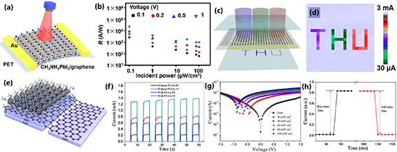
Figure 9. (a) Schematic illustration of CH3NH3PbI3/graphene heterostructure-based flexible PD. (b) Photoresponsivity of the device under different applied voltages and illumination power. (c) Schematic diagram of the flexible image sensor using CH3NH3PbI3/graphene heterostructure. (d) The corresponding output image under different light illumination (380, 633 and 750 nm of power 75 mW). Reprinted from [113], Copyright (2020), with permission from Elsevier. (e) Schematic of the device configuration of perovskite/graphene/TiO2/FTO self-powered PD. (f) Temporal photoresponse of the PD with and without PTAA operated with external bias of 1 V and without bias voltage. (g) Temporal response of the PD showing photocurrent rise and fall time of 5 ms. Reprinted with permission from [114]. Copyright (2017) American Chemical Society.
Download figure:
Standard image High-resolution imageThough the above-mentioned perovskite/graphene hybrid PDs show very high responsivity with high photoconductive gain, an external power source is essential for their operation. Interestingly, the self‐powered PDs that can work without an external power source has great application potential in next‐generation devices that can operate wirelessly and independently are being studied extensively [115, 116]. Li et al reported a self-powered TiO2/graphene/CH3NH3PbI3 perovskite PD [114]. The graphene layer forms a Schottky junction with TiO2 that can efficiently separate and transport photogenerated excitons at the graphene/perovskite interface with superior device performance. The device configuration of the self-powered PD is shown in figure 9(e). The photoswitching behavior of the PD with and without bis(4-phenyl)(2,4,6-trimethylphenyl)amine (PTAA) HTL under 560 nm light with a power density of 40 mW cm−2 at 0 V (no bias) is shown in figure 9(f). The PD exhibits a photocurrent of 0.2 mA under self-powered mode. The I−V characteristics of the PD under solar simulator illumination at different light intensities are shown in figure 9(g). The self-powered device shows photocurrent rise time and fall time of ∼5 ms (figure 9(h)). Thus, the self-powered device showed fast photoresponse as compared to the other reported perovskite/graphene-based phototransistor.
The 0D graphene QDs (GQDs) have a tunable bandgap due to the quantum confinement of carrier and edge effects [117, 118]. Interestingly, the structural, optical, and electrical properties of GQDs can be simply tuned by chemical doping for high-performance GQDs based optoelectronics [119]. Algadi et al demonstrated NGQDs/all-inorganic cesium lead bromide perovskite NCs heterostructure PD, which exhibits a responsivity of 0.24 A W−1, specific detectivity of 2.5 × 10¹² Jones, and on/off ratio of 7.2 × 10⁴ [114]. Subramanian et al reported TiO2/CH3NH3PbI3/GQDs hybrid PD, which shows a photoresponsivity of 12 A W−1, and a detectivity up to 6.5 × 10¹¹ Jones [120]. In this device, GQDs serve as HTL, while TiO2 serves as ETL, which effectively increases the carrier separation in the perovskite layer. A summary of the performance parameters of the reported metal halide perovskite/graphene based PDs is presented in table 1. However, as the fabrication method, device configuration and device interfaces are different for different cases, so the comparison is not straightforward. It is apparent that the CH3NH3PbI3−x Clx film/P3HT/graphene photo FET possesses the highest photoresponsivity and a quite high gain in the device.
Table 1. Summary of performance parameters of reported metal halide perovskite/graphene PDs.
| Device structure | Responsivity (A/W) | Detectivity (Jones) | Rise time/fall time (s) | Gain | EQE (%) | Reference |
|---|---|---|---|---|---|---|
| CH3NH3PbI3 film/graphene photo FET | 180 | 109 | 0.087/0.54 | — | 5 × 10⁴ | [85] |
| CH3NH3PbBr2I islands/graphene photo FET | 6.0 ×10⁵ | — | 0.12/0.75 | 109 | — | [86] |
| CH3NH3PbI3 nanowire/graphene photo FET | 2.6 × 10⁶ | — | 55/75 | — | — | [87] |
| CH3NH3PbI3/graphene/Au NP photo FET | 2 × 10³ | — | 1.5/- | — | ∼8 × 10³ | [94] |
| CH3NH3PbI3−x Clx film/P3HT/graphene photo FET | 4.3 × 10⁹ | — | — | 8.9 × 10⁹ | — | [95] |
| CH3NH3PbI3-PCBM BHJ film/graphene photo FET | 8 × 10⁵ | — | 92/6203 | — | — | [96] |
| 2D multiphase perovskite/graphene/(hBN) photo FET | ∼105 | 3.3 × 10¹⁰ | <0.2 | — | — | [20] |
| CH3NH3PbI3/graphene flexible photo FET | 115 | 3 × 10¹² | — | — | — | [99] |
| Graphene/CH3NH3PbI3/graphene barristor-type photo FET | 950 | — | 0.022/0.037 | 2200 | — | [100] |
| Vapor deposited CH3NH3PbI3 film/graphene photo FET | 1.73 × 10⁷ | 2 × 10¹⁵ | 0.879 | 106 | — | [101] |
| CH3NH3PbI3–PbS QDs/graphene flexible photo FET | 2 × 10⁵ | 5 × 10¹² | ∼0.5-1 | 107 | — | [102] |
| NGQDs–CH3NH3PbI3/mrGO photo FET | 1.92 × 10⁴ | 2.71 × 10¹³ | 0.013/0.010 | 104 | — | [103] |
| Graphene/CH3NH3PbI3 perovskite/graphene Schottky junction PD | 0.022 | 3.55 × 10⁹ | — | 2.64 × 10³ | — | [104] |
| CH3NH3PbBr3/N-rGO hybrid PD | 3.6 × 10⁴ | 1012 | 0.030/0.10 | — | >105 | [105] |
| CsPbBr3−x Ix NCs/graphene photo FET | 8.2 ×10⁸ | 2.4 × 10¹⁶ | 0.81/3.65 | — | — | [109] |
| FAPbBr3 QDs/graphene photo FET | 1.15 × 10⁵ | 0.058/0.60 | 3.42 × 10⁷ | [110] | ||
| CsPbBrx I3−x NCs/graphene photo FET | 1.1 3 × 10⁴ | 1.17 × 10¹¹ | 0.273/2.26 | 9.32 × 10¹⁰ | — | [111] |
| CH3NH3PbI3/graphene flexible PD | 2.7 × 10³ | — | — | — | — | [113] |
| TiO2/graphene/CH3NH3PbI3 self-powered PD | 0.375 | ∼1011 | <0.005 | — | — | [114] |
2.2. Perovskite/TMDs photodetector
One of the major shortcomings of pure graphene in heterojunction PD and other optoelectronics is its zero bandgap and metallic nature. Thus, most of the reported graphene/perovskite PDs are photo–FET or Schottky junction type. On the other hand, TMDs such as MoS2, WS2, MoSe2, and WSe2 with a 2D semiconducting structure, are considered to be promising nanomaterials for future electronic and optoelectronic applications [3, 119, 121–131].
2.2.1. Perovskite/MoS2 photodetector
In 2016, Kang et al first reported a perovskite/MoS2 hybrid phototransistor in which CH3NH3PbI3 perovskite acted as a light-harvesting photoactive layer and mechanically exfoliated multilayer MoS2 was adopted as a charge transporting layer [132]. Additionally, they applied APTES surface treatment to SiO2/Si, which resulted in the n-doping of MoS2 and suppressed the recombination rate of photogenerated carriers in the perovskite layer (figure 10(a)). The responsivity and detectivity of perovskite/MoS2/APTES hybrid photo FET were observed to be 2.11 × 10⁴A W−1 and 1.38 × 10¹⁰ Jones, respectively (figure 10(b)). The responsivity of the photo FET decreases at 785 nm, which matches with the absorbance of the perovskite layer. The comparison of photocurrent growth and decay times of MoS2, MoS2/APTES, and perovskite/MoS2/APTES PDs are shown in figure 10(c). The perovskite/MoS2/APTES device showed the fastest response of 6.17 and 4.5 s of rise and fall time, respectively. The improved photoresponse of the device with APTES was due to (a) the addition of APTES prevented the higher recombination rate of carriers by the interfacial traps at MoS2/SiO2 junction, and (b) the n-doping reduced the carrier recombination rate in the MoS2. However, the reported PDs showed low responsivity and slow photoresponse speed compared to the other reported MoS2/perovskite-based PDs, which may be due to defects and poorer morphology of perovskite film.

Figure 10. (a) Schematic illustration of the perovskite/MoS2/APTES phototransistor and cross-sectional structure explaining the APTES-doping mechanism on the MoS2 film. (b) Photoresponsivity and detectivity of the device as a function of incident light power. (c) Comparison of photocurrent rise and fall times of MoS2, MoS2/APTES, and perovskite/MoS2/APTES PDs. [132] John Wiley & Sons. [© 2016 WILEY‐VCH Verlag GmbH & Co. KGaA, Weinheim]. (d) Schematic illustration of the device configuration of perovskite/MoS2 PD. (e) Energy band diagram and charge transfer mechanism from perovskite to 1 T and 2 H phases of MoS2. (f) Spectral responsivity and EQE of CH3NH3PbI3/1 T-MoS2 PD. (g) Spectral responsivity and EQE of CH3NH3PbI3/2 H-MoS2 PD. (h) Responsivities of PD with the 1 T phase of MoS2 as a function of various illumination powers. (i) Temporal photoresponse of CH3NH3PbI3/1 T-MoS2 PD. (j) Temporal photoresponse of CH3NH3PbI3/2 H-MoS2 PD. [133] John Wiley & Sons. [© 2016 WILEY‐VCH Verlag GmbH & Co. KGaA, Weinheim].
Download figure:
Standard image High-resolution imageWang and co-workers demonstrated solution-processed CH3NHH3PbI3/MoS2 heterostructure PD using the semiconducting and metallic phase of MoS2 [133]. MoS2 can exist in two phases: (a) the trigonal prismatic (2H phase) crystal structure with semiconducting behavior, and (b) the octahedral (1T phase) crystal structures with metallic behavior. The 1T phase of MoS2 is metastable and can be transformed into the thermodynamically stable 2H-MoS2 phase by annealing. MoS2 nanosheets (NSs) were fabricated by the chemical exfoliation method form bulk MoS2. Perovskite/MoS2 NS PD is illustrated in figure 10(d). Energy band diagrams of CH3NH3PbI3/MoS2 and the carrier transfer mechanisms in the metallic 1T and semiconducting 2H phase of MoS2 are shown in figure 10(e). In the case of the 1T phase of MoS2, both photogenerated electrons and holes can be injected from photoactive perovskite to the MoS2 layer, leading to the recombination of charges in the layer (figure 10(e)). However, due to the higher current in the device with metallic 1T phase of MoS2 compared to the PD with 2H phase, higher photoresponsivity with low on/off ratio was observed. In the case of the perovskite/2H-MoS2 PD, photo-induced electrons and holes are injected from the perovskite into the conduction and valence bands of the 2H phase MoS2, respectively (figure 10(e)), and the electrons and holes transfer to the electrodes due to the Schottky barrier at the contacts. The spectral responsivity and EQE of the devices with 1T-MoS2 and 2H-MoS2 are shown in figures 10(f) and (g). As compared to the PD with the 2H phase, PD with the 1T phase shows higher photoresponsivity due to the injection of a higher concentration of charges due to the metallic nature of 1T-phase. The PD with the 1T phase exhibits a responsivity of 3.09 × 10³ A W−1 and an EQE of 7.7 × 10⁵%. The photoresponsivity decreased at ∼800 nm due to the decrease in the absorbance of perovskite active layer. Power-dependent responsivity and detectivity of the device with the 1T phase of MoS2 under the illumination of the light of wavelength 500 nm is shown in figure 10(h). The device exhibits photoresponsivity of 3.3 × 10⁵ A W−1 at a power of 0.14 µW (figure 10(h)). The temporal photoresponse of the PD with 1T and 2H phase of MoS2 are shown in figures 10(i) and (j), respectively. The rise and decay times were measured to be 0.45 and 0.75 s for PD with 1T phase (figure 10(i)), respectively, while the same for the 2H phase were observed to be <25 and 50 ms, respectively (figure 10(j)). It was believed that the higher defects in the 1T phase of MoS2 led to the trapping of photocarriers, resulting in slower response speed. However, the reported photoresponsivity was very high compared to other perovskite/MoS2 based photo FETs.
Peng et al demonstrated a solution-processed phototransistor utilizing CH3NH3PbI3 perovskite–MoS2 BHJ as the active material and a reduced graphene oxide (rGO) layer as the transporting layer as illustrated in figure 11(a) [134]. The energy band diagram of the hybrid system is illustrated in figure 11(b), showing the transfer process of photogenerated carriers. The photo-induced electrons in perovskite transferred to MoS2 avoiding the radiative recombination, while holes transferred from perovskite to the rGO channel, which resulted in an increased photocurrent (figure 11(b)). Thus, with the introduction of MoS2, the carrier separation and transport was significantly improved in the photoactive layer. The phototransistor with MoS2 exhibits a responsivity of 1.08 × 10⁴ A W−1 at VGS = 0 V and VDS = 2 V, at an incident power density of 0.53 μW cm−2, which is about five times higher than that of the device without MoS2 (figure 11(c)). The specific detectivity of the hybrid device was calculated to be 4.28 × 10¹³ Jones (figure 11(c)). Thus, these PDs exhibited higher detectivity than the other perovskite/MoS2 based PDs.
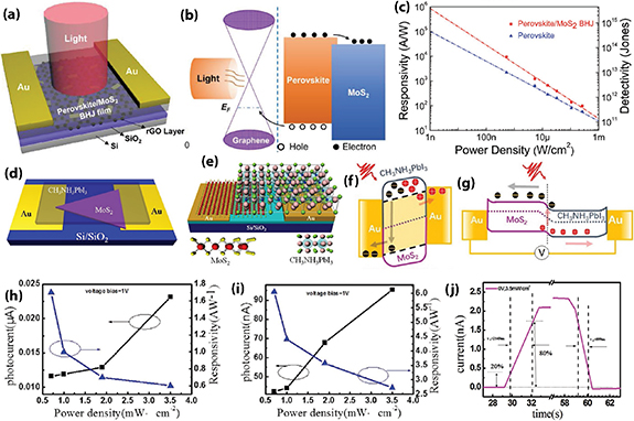
Figure 11. (a) Device structure of rGO/CH3NH3PbI3–MoS2 BHJ phototransistor. (b) Energy level diagram showing the carrier transfer process in the of rGO/CH3NH3PbI3–MoS2 BHJ hybrid structure. (c) Variation of responsivity and detectivity of the devices as a function of incident power at 660 nm in presence and absence of MoS2 layer under VGS = 0 V, VDS = 2 V. [134] John Wiley & Sons. [© 2018 WILEY‐VCH Verlag GmbH & Co. KGaA, Weinheim]. (d) Schematic illustration of planar type CH3NH3PbI3/MoS2 PD. (e) Schematic structure of the vertical type CH3NH3PbI3/MoS2 PD. Energy band diagram under the illumination of (f) planar PD (g) vertical PD. (h) Temporal photoresponse of self-powered vertical PD. [135] John Wiley & Sons. [© 2018 WILEY‐VCH Verlag GmbH & Co. KGaA, Weinheim].
Download figure:
Standard image High-resolution imageBai and co-workers fabricated a self-powered PD based on a CH3NH3PbI3 perovskite/monolayer MoS2 vertical type heterojunction [135]. They also investigated the performance of the device with a planar structure configuration. Monolayer MoS2 was synthesized on SiO2/Si substrates by the CVD method. Figure 11(d) presents a schematic illustration of CH3NH3PbI3/MoS2 planar structure PD in which the electrodes are bonded to two different materials. The schematic structure of CH3NH3PbI3/MoS2 vertical type heterojunction PD is shown in figure 11(e) in which one electrode is connected to MoS2, and another electrode is connected to the CH3NH3PbI3 film. The band alignment of planar and vertical PD under light illumination are shown in figures 11(f) and (g), respectively. In the case of planar structure device, under photon irradiation, electron–hole pairs are generated in the photoactive perovskite film, and these electrons are transferred to MoS2 film, which increases the Fermi level of MoS2 and reduces the Schottky barriers between Au electrode and material, causing the high photocurrent of the device (figure 11(f)). For vertical heterojunction devices, under illumination, the photogenerated electrons are transferred to the MoS2 side, while holes are transferred to the perovskite side figure 11(g). Due to the suitable band alignment and built-in potential across the heterojunction, the vertical PD can operate without any external bias. The excitation intensity-dependent photocurrent and responsivity of the planar and vertical device are shown in figures 11(h) and (i), at a bias of 1 V, respectively. The planar and vertical type PD device exhibit a responsivity of 28 and 68.11 A W−1, respectively, at illumination intensity of 0.7 mW cm−2 and a voltage bias of 5 V. The photocurrent growth and decay times for the vertical self-powered device were found to be 2149 and 899 ms, respectively (figure 11(j)). However, the photoresponse speed of this device is relatively slow which may be due to the traps and defects.
Chandrasekar et al synthesized solution-processed CH3NH3PbI3: MoS2 nanohybrid for photodetection [136]. The interfacial carriers transfer between the 2D MoS2 NS and perovskite cuboid heterojunction are utilized to enhance the device performance. The Au/CH3NH3PbI3: MoS2/Au PD exhibits responsivity of 696 mA W−1 with the response speed of 50/16 ms (photocurrent growth/decay), while pristine Au/CH3NH3PbI3/Au PD shows responsivity of 312 mA W−1 with the response speed of 73/60 ms (photocurrent growth/decay). The device with MoS2 also exhibits a very low dark current as compared to the pristine device.
He and co-workers fabricated lead-free (CH3NH3)3Bi2Br9 perovskite/MoS2 PD [137]. MoS2 NSs were synthesized by scotch tape exfoliation method, while the perovskite layer was deposited by simple solution process technique. (CH3NH3)3Bi2Br9-coated MoS2 PD exhibit photoresponsivity of 112 A W−1, detectivity of 3.8 × 10¹² Jones, and photoresponse time of 0.3 ms.
Wang et al reported self-powered CH3NH3PbI3/2D BP/MoS2 hybrid 2D photogate photodiode [138]. The schematic diagram of a 2D photogate photodiode is shown in figure 12(a). The electronic band structure of the heterojunction PD demonstrates type I and type II heterojunctions formation at the CH3NH3PbI3/BP and BP/MoS2 interfaces, respectively (figure 12(a)). Due to the lower exciton binding energy in perovskite materials, excitons can easily dissociate [139]. In the presence of light, the photocarriers are spontaneously generated in the CH3NH3PbI3 perovskite film, which further diffuses into the underlying BP layer followed by carriers separation and collection due to the existence of a built-in electric field at the BP/MoS2 junction (figure 12(b)). Thus, the observed photocurrent of the device is determined by the photoactive perovskite layer and photocarrier separation/transport at the BP/MoS2 interface. The I–V characteristics of the device show a typical diode-like rectifying behavior with a rectification ratio of 20 (figure 12(b)). In figure 12(c), the solid lines correspond to the dark current, while the dotted lines represent the photocurrent of the device. Due to the increase in electric field under reverse bias, the photocurrent was increased. The temporal photoresponse for CH3NH3PbI3/BP/MoS2 PD at −2 V is shown in figure 12(d). The photocurrent growth and decay times were observed to be 150 and 240 μs, respectively. The responsivity of the PD was calculated to be 11 A W−1 under the illumination of 457 nm laser of intensity 0.02 mW cm−2 and the highest photocurrent on–off ratio was reported to be ∼6 × 10⁴ at 119 mW cm−2 under 2 V reverse bias (figure 12(e)). Due to the built-in potential, the device can also operate without any external bias. The photocurrent switching performance at a different incident wavelength and intensity of 100 mW cm−2 shown in figure 12(f) depicts the good photoswitching behavior of the self-powered PD. Thus, this report is significant for self-powered perovskite/MoS2 based PDs.

Figure 12. (a) Schematic illustration of CH3NH3PbI3/2D BP/MoS2 hybrid photodiode. (b) Band diagram and photocarriers transfer mechanism of the photogate photodiode. (c) I−V characteristics of CH3NH3PbI3/2D BP/MoS2 PD. The solid lines and dashed lines represent the dark current and photocurrent of the device. (d) Temporal photoresponse of perovskite/BP/MoS2 PD. (e) Variation of photoresponsivity and on/off ratio of the PD with incident light intensity at a reverse bias of 2 V. (f) Dynamic photoresponse of PD at different wavelengths of intensity 100 mW cm−2 under zero bias. Reprinted with permission from [138]. Copyright (2019) American Chemical Society. (g) Schematic structure of graphene/(PEA)2SnI4 2D perovskite/MoS2/graphene PD. (h) Power-dependent responsivity and EQE of the PD at zero bias. (i) Transient photocurrent response of the device at zero bias. Reprinted with permission from [140]. Copyright (2019) American Chemical Society.
Download figure:
Standard image High-resolution imageFang et al fabricated lead-free 2D Ruddlesden–Popper perovskites/MoS2 vertical heterojunction PD [140]. They used few layers n-type MoS2 and p-type (PEA)2SnI4 (where PEA = C6H5C2H4NH3) 2D perovskite in the heterojunction PD, while graphene serves as electrodes for the device, as illustrated in figure 12(g). Due to the suitable band alignment and built-in potential, the heterojunction PD can operate without any external bias. The variation of responsivity and EQE of the heterojunction PD with incident light intensity at 451 nm under zero bias is shown in figure 12(h). The maximum responsivity and EQE were observed to be 121 mA W−1 and 38.2% under the illumination of power 36 pW. They also reported the responsivity of 1100 A W−1 at 3 V. The self-powered device shows photocurrent rise time and fall time of 34 and 38 ms, respectively (figure 12(i)). However, responsivity of the device was relatively low compared to the other reported results.
Sun et al reported perovskite PD based on triple cation mixed-halide perovskite layer and CVD grown atomically thin MoS2 layer, as illustrated in figure 13(a) [141]. The MoS2 layer was grown by the CVD process, while triple cation Cs0.05(MA0.17FA0.83)0.95Pb(I0.83Br0.17)3 was deposited by simple solution process technique. The variation of responsivity and photocurrent of the device with incident light power at wavelength 520 nm and 2 V of applied bias is shown in figure 13(b). The PD exhibits a responsivity of 342 A W−1 and detectivity of 1.14 × 10¹² Jones at incident power of 2.2 pW. The photocurrent rise and fall times were observed to be 27 and 21 ms, respectively (figure 13(c)). They also fabricated devices on flexible PET substrate, which showed stability up to 20000 bending cycles. These results are significant for the realization of flexible PDs.
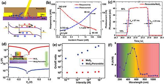
Figure 13. (a) Working mechanism and energy-band diagram of triple cation perovskite/MoS2 hybrid PD. (b) Variation of photocurrent and responsivity with incident light power. (c) Temporal photocurrent response of the hybrid device. Reprinted from [141], Copyright (2019), with permission from Elsevier. (d) Comparison of dark current of bare MoS2 and MoS2/(PEA)2PbI4 hybrid PD. The inset shows a schematic of the device configuration of hybrid PD. (e) Intensity dependent of on/off ratio of MoS2 and MoS2/(PEA)2PbI4 PD. (f) Spectral responsivity of the MoS2/(PEA)2PbI4 hybrid PD. [142] John Wiley & Sons. [© 2020 WILEY‐VCH Verlag GmbH & Co. KGaA, Weinheim].
Download figure:
Standard image High-resolution imageWang et al recently demonstrated (C6H5C2H4NH3)2PbI4 2D halide perovskite/MoS2 hybrid PD with a very low dark current figure 13(d) [142]. Multilayer MoS2 flakes were synthesized by the mechanical exfoliation method and transferred on the SiO2/Si substrates. 2D hybrid perovskite was deposited on MoS2 by solution process spin coating technique. The dark current of (PEA)2PbI4/MoS2 PD was significantly suppressed compared to the pristine MoS2 PD, which effectively increased the on/off ratio. Figure 13(e) shows the comparison of the on/off ratio of pristine MoS2 PD and (PEA)2PbI4/MoS2 PD for different intensity of light illumination. The on/off ratio of perovskite/MoS2 PD was found to be ∼105 (figure 13(e)). The spectral responsivity of the device at 0.06 nW is shown in figure 13(f). The hybrid PDs showed good responsivity in the wavelength range 200–650 nm. The device exhibits a specific detectivity of 1.06 × 10¹³ Jones at 0.1 nW. Note that the ambient stability of 2D halide perovskite-based PDs is much higher than the 3D perovskite-based PDs, which is beneficial for their practical applications.
Compared to the organic–inorganic hybrid perovskite, all-inorganic perovskite NCs and QDs show superior ambient stability [143, 144]. Song et al reported all-inorganic CsPbBr3 NSs/2D MoS2 heterostructure PD [145]. Monolayer MoS2 was synthesized by a CVD process and then transferred onto SiO2/Si substrates. The CsPbBr3 NSs were then drop-cast on MoS2 on Si/SiO2, followed by annealing at 60 °C. The device configuration of CsPbBr3 NSs/MoS2 PD is shown in figure 14(a). The type-II heterojunction formation between CsPbBr3 NSs and MoS2 PD helps in better carrier separation suppressing the radiative recombination. Under light illumination, electron–hole pairs are generated in the photoactive perovskite NSs, and due to the strong driving force of the built-in electric field, these photogenerated electrons are transferred to the monolayer MoS2, whereas the holes are confined in the perovskite NSs (figure 14(b)). This results in superior photodetection in the hybrid device. The I−V characteristics of the hybrid PD as a function of the illumination intensity at 442 nm are shown in figure 14(c). Under the illumination, the current increases dramatically, and the on/off ratio was calculated to be more than 104. The responsivity of the CsPbBr3 NSs/MoS2 PD device was increased nearly 20 or 1000 times compared with that of the CsPbBr3 or bare MoS2 PD at different intensities of incident light (figure 14(d)). The hybrid PD exhibits a photoresponsivity of 4.4 A W−1, a detectivity of 2.5 × 10¹⁰ Jones, and EQE of 302%. The hybrid PD showed good photoresponsivity up to 550 nm due to the absorption of CsPbBr3. The spectral responsivity of the hybrid PD at different applied bias matches well with the absorbance of photoactive CsPbBr3 NSs (figure 14(e)). The photocurrent rise and fall times of the hybrid PD were observed to be 0.72 and 1.01 ms, respectively (figure 14(f)). Overall, the photoresponsivity of the device was relatively low, which may be due to the traps at the perovskite/MoS2 interface.
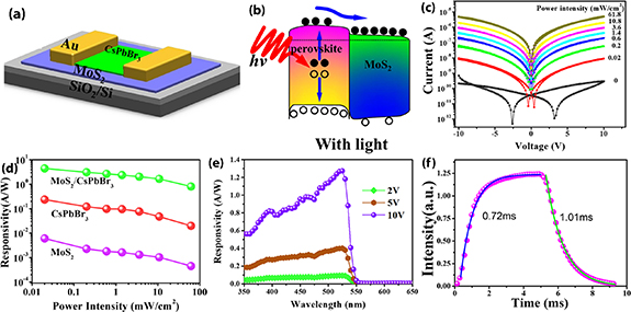
Figure 14. (a) Schematic illustration of CsPbBr3 NSs/MoS2 hybrid PD. (b) Photogenerated charge transfer process in CsPbBr3/MoS2 heterojunction. (c) I–V characteristics of the hybrid device in the dark and under 442 nm laser illumination with different intensities. (d) Comparison of photoresponsivity with the light intensity of pristine MoS2, CsPbBr3 and hybrid PD. (e) Wavelength-dependent responsivity of the hybrid device at 2, 5, and 10 V of applied bias. (f) Temporal photoresponse of the hybrid device showing rising and decay times. Reprinted with permission from [145]. Copyright (2018) American Chemical Society.
Download figure:
Standard image High-resolution imageNoh et al reported CsPbBr3 QDs/monolayer MoS2 phototransistor [146]. CsPbBr3 QDs were synthesized by the hot injection method, while monolayer MoS2 was grown by the CVD process [147]. They suggested significant transfer of photogenerated electron form perovskite QDs to MoS2 and n doping of MoS2, which effectively increased the performance of the device. The hybrid photoFET exhibits a responsivity of ∼1 A W−1, which is nearly independent of the incident light intensity.
Lin and co-workers fabricated CsPbBr3 QDs/few-layer MoS2 phototransistor, which exhibited a high photoresponsivity of 104A W−1 and a fast photoresponse speed of 8 ms [148].
Liu et al reported MoS2 QDs encapsulated in a CH3NH3PbI3 perovskite film for photo FET application, which showed a high detectivity of 5 × 10¹¹ Jones and a response speed of 25 μs [149].
Wu et al fabricated CsPbI3−x Brx QDs/monolayer MoS2 phototransistor [150]. Monolayer MoS2 was grown by an oxygen-assisted CVD process and transferred onto SiO2/Si substrate by PMMA-assisted transfer method, while mixed halide all-inorganic perovskite QDs were synthesized by hot injection method. The schematic illustration of the device is presented in figure 15(a), and the inset of the figure shows the TEM image of perovskite QDs. The favorable type II band alignment facilitating interfacial photogenerated charge separation and efficient carrier injection into the MoS2 result in superior photodetection of the hybrid system. Under light illumination, electron–hole pairs were generated in the highly light-absorbing perovskite QDs layer and then separated by the built-in field produced at the interface of the heterojunction (figure 15(b)). The photogenerated electrons were transferred to the MoS2 side, while holes moved to the QDs side, suppressing radiative recombination. The transfer characteristics of the phototransistor under 532 nm illumination with different optical powers is presented in figure 15(c). The photocurrent increases with illumination power. The photo FET exhibits a high responsivity of 7.7 × 10⁴ A W−1, an EQE exceeding 107%, and a specific detectivity of ∼5.6 × 10¹¹ Jones at a VG of 60 V (figure 15(d)). The photocurrent rise and fall times were observed to be 0.59 and 0.32 s, respectively, at Vd = 0.1 V (figure 15(e)). Though their device showed very high responsivity, the temporal response was relatively slow.

Figure 15. (a) Schematic illustration of CsPbI3−x Brx QDs/monolayer MoS2 phototransistor. (b) Energy level diagrams of CsPbI3−x Brx QDs/MoS2 heterostructure. (c) Transfer characteristics of the device under different illumination power. (d) Responsivity, detectivity and EQE of CsPbI3−x Brx QDs/MoS2 PD. (e) Temporal photoresponse of the device showing photocurrent growth and decay times. Reproduced from [150]. CC BY 4.0. (f) Schematic illustration of CsPbBr3 NCs/monolayer MoS2 PD. (g) Band structure and charge transfer in CsPbBr3/MoS2 heterostructure. (h) EQE and detectivity of the device as a function of perovskite NCs solution concentration. (i) Dependence of photocurrent growth and decay times on perovskite solution concentration. (j) Photocurrent and responsivity as a function of perovskite NCs purifying treatment cycles. (k) Dependence of photocurrent growth and decay times as a function of NCs purifying treatment cycles. [151] John Wiley & Sons. [© 2019 WILEY‐VCH Verlag GmbH & Co. KGaA, Weinheim].
Download figure:
Standard image High-resolution imageZhang and co-workers tuned optoelectronic properties of all inorganic CsPbBr3 perovskite NCs by regulating solution concentration and surface ligand content for perovskite NCs/MoS2 hybrid PDs [151]. The device configuration is presented in figure 15(f). The band structure and photogenerated electron transfer from perovskite NCs to MoS2 are presented in figure 15(g). The variation of EQE and detectivity of the device with perovskite QDs concentration is shown in figure 15(h). With the increase of concentration of perovskite solution, the light absorption capability was effectively increased, which results in a more effective process of exciton dissociation and charge transport at the interface leading to an improved photocurrent response of the PD. The responsivity, EQE, and detectivity were observed to be 6.40 × 10⁵ mA W−1, 1.50 × 10⁵%, and 3.38 × 10¹¹ Jones, respectively. Perovskite QDs concentration–dependent photocurrent growth and decay times are presented in figure 15(i). Owing to the efficient separation and transport of the charge carriers at the interface, the response rate became faster in the hybrid system. For the synthesis of perovskite NCs/QDs, different surfactants, ligands such as oleic acid and oleylamine are used, which are beneficial for surface passivation and elimination of defects [152, 153]. However, an excessive amount of ligands blocks charge transfer across the interface by forming an insulating layer in a device. The author investigated the regulation effects of surface ligands with different purifying treatment cycles. With the increase of purifying cycles, the perovskite NCs may be degraded and aggregated, which results in poor device performance (figures 15(j) and (k)).
2D MoS2 has also been used in different perovskite solar cells as a charge transport layer, which efficiently increases carrier separation and transport, leading to high PCE [154–157]. In a recent work, Ghosh et al demonstrated a monolayer MoS2/CsPbBr3 NCs type-II vertical heterojunction PD [158]. All inorganic CsPbBr3 NCs were synthesized by room-temperature, two-step solid-state synthesis method. Large area monolayer MoS2 film was grown directly on a SiO2/Si substrate by the CVD method. The schematic of the vertical heterojunction PDs is shown in figure 16(a); the inset of the figure depicts the cross-sectional FESEM image of the heterojunction device. Based on the band alignment, MoS2 and CsPbBr3 form a type-II heterojunction. Under illumination, electron and hole pairs are generated in CsPbBr3 NCs, and these electrons are transported to MoS2. Thus, separation and transport of excitons suppressing radiative recombination in the perovskite lead to the high photocurrent of the device with fast photoresponse speed. The quenching of the PL intensity of perovskite in the heterostructure with MoS2 device as compared to the pristine CsPbBr3 NCs film provided evidence that indeed there is transfer and separation of photogenerated carriers from perovskite NCs to MoS2 (figure 16(b)). TRPL spectra related to perovskite NPs also confirmed charge transfer, as shown in the inset of figure 16(b). Under the reverse bias, the photocurrent of the device was increased significantly, as shown in figure 16(c), which was attributed to the suitable band bending at the heterojunction enabling superior charge separation and transport. The comparison of spectral photoresponsivity of the heterojunction PDs and pristine MoS2 PDs are shown in figure 16(d). The vertical heterojunction PD exhibit responsivity of 6.7 A W−1 at 400 nm of incident light, which is significantly higher than the pristine MoS2 PD. The responsivity of the heterojunction PD as a function of incident light intensity is shown in the inset of figure 16(d). The variation of the photocurrent as a function of incident light intensity is shown in figure 16(e). The rise time and fall time of the heterojunction PD were observed to be 5.48 and 24.01 μS, respectively (figure 16(f)) which is significantly faster than the pristine MoS2 PD. Thus, the high photoresponsivity and fast photoresponse speed were attributed to the superior charge separation and transport in the type–II heterojunction device. The detection range of the PD was 300–540 nm. The above conclusion was supported by the density functional calculation of the electronic structure of the pristine and hybrid systems.
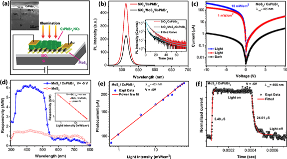
Figure 16. (a) Schematic illustration of monolayer MoS2/CsPbBr3 NCs vertical heterojunction PD. The inset depicts a cross-sectional FESEM image of the device. (b) Comparison of the PL spectra of CsPbBr3 NCs films on the MoS2 layer and the SiO2 substrate. The inset shows a variation of the time resolved PL decay profiles of the two samples. (c) I–V characteristics of the heterojunction PD under dark and illumination with different intensities. (d) Spectral photoresponsivity of the heterojunction and pristine MoS2 device in the wavelength 300–800 nm under 5 V bias. The inset shows the photoresponsivity of the PD as a function of the incident light intensity. (e) Variation of photocurrent with illumination intensity and its fitting with the power law. (f) Temporal photoresponse of the heterojunction PD showing rise and fall times. Reproduced from [158] with permission of The Royal Society of Chemistry.
Download figure:
Standard image High-resolution image2.2.2. Perovskite/WS2 photodetector
Monolayer WS2 having a higher direct bandgap than monolayer MoS2, has receive major attention for various optoelectronic applications. In 2016, Ma et al first integrated monolayer WS2 with perovskite to improve the photodetection performance in planar PDs [159]. Monolayer WS2 was deposited by the CVD method on clean C-plane sapphire substrates, while CH3NH3PbI3 perovskite films were deposited onto the monolayer WS2 using sequential vapor deposition and vapor annealing method. A schematic device structure of the hybrid CH3NH3PbI3/WS2 planar PD fabricated on a sapphire substrate is presented in figure 17(a). The energy band structures of the CH3NH3PbI3/WS2 hybrid system is illustrated in figure 17(b). In the presence of light, electrons-hole pairs are generated in the photoactive perovskite layer, and due to the difference between their Fermi levels, these photogenerated charges are transferred to monolayer WS2, which reduces the carrier recombination and enhances the photodetection performance [160, 161]. With the increase in the power of incident light, photocurrent increases and the symmetric I–V curves of CH3NH3PbI3/WS2 PD indicate Ohmic–like contacts between the photoconductors and the electrodes (figure 17(c)). In the hybrid device with WS2, dark current was observed one order of magnitude lower than the pristine perovskite PD due to defects and interfacial carrier transfer lowering the charge concentration in the depletion region. The device exhibits a responsivity of 17 A W−1 under a bias of 5 V and a light intensity of 0.2 μWcm−2 (figure 17(d)). The maximum on/off of the device was observed to be 3 × 10⁵. The rise and decay times of photocurrent were measured to be 2.7 and 7.5 ms, respectively (figure 17(e)).
Figure 17. (a) Schematic of device structure of the hybrid CH3NH3PbI3/WS2 PD fabricated on a sapphire substrate. (b) The energy level of CH3NH3PbI3/WS2 heterostructure. (c) I–V characteristics of the hybrid PD measured in dark and under illumination with white-light at different intensities. (d) Variation of photocurrent and responsivity with incident light intensity. (e) Temporal photoresponse of the device showing photocurrent growth and decay times. [159] John Wiley & Sons. [© 2016 WILEY‐VCH Verlag GmbH & Co. KGaA, Weinheim]. (f) I–V curves of the CH3NH3PbI3/WS2 hybrid PD under dark and white-light. The inset shows the schematic diagram of CH3NH3PbI3/WS2 hybrid PD. (g) Variation of responsivity and detectivity of the device with illumination intensity. (h) Spectral responsivity and detectivity of CH3NH3PbI3/WS2 hybrid PD. (i) Temporal photoresponse of CH3NH3PbI3/WS2 and bare CH3NH3PbI3 PD. Reprinted with permission from [162]. Copyright (2018) American Chemical Society.
Download figure:
Standard image High-resolution imageLi et al studied the light-matter interactions and mechanism of photogenerated carrier transfer from CH3NH3PbI3 to atomically thin WS2 by conductive and photoconductive atomic force microscopy [162]. They further fabricated CH3NH3PbI3/WS2 hybrid PD. Under illumination at 532 nm, they observed a significant increase in photocurrent in CH3NH3PbI3/WS2 heterostructure compared with the bare CH3NH3PbI3 regions from the spatially resolved photocurrent images. The I–V characteristics of CH3NH3PbI3/WS2 heterojunction PD show photovoltaic behavior with an open-circuit voltage of ∼0.3 V and photocurrent was increased with the increase in illumination intensity (figure 17(f)). The PD exhibited a responsivity of 76.7 mA W−1 and a detectivity of 3.40 × 10⁹ Jones under illumination intensity of 0.09 mW cm−2 and 2.5 V of applied bias (figure 17(g)). The incident light wavelength-dependent responsivity and detectivity match well with the absorbance of the photoactive perovskite layer (figure 17(h)). With the illumination of 405 nm, photoresponsivity and detectivity of the PD were measured to be 3.9 mA W−1 and 1.81 × 10⁸ Jones, respectively. The photocurrent rise and decay times were found to be 13.5 and 18.7 ms, respectively, which is faster than the bare perovskite PD due to the efficient photogenerated carrier separation at the interface between WS2 and perovskite (figure 17(i)). Thus, the photoresponsivity of the device was quite low compared to the other reported devices.
Zhang et al demonstrated phototransistors using CH3NH3PbI3 perovskite-WS2 NS composite as optical absorber and rGO as a channel layer [163]. The photo FET exhibits photoresponsivity of 678.8 A W−1, specific detectivity of 4.99 × 10¹¹ Jones and EQE value of 2.04 × 10⁵%. The superior photodetection performance of the device is attributed to electron trapping by the WS2 NSs resulting in photo-generated electron–hole separation and high carrier mobility of the rGO channel. Thus, the device showed very high photoresponsivity compared to the other reported perovskite/WS2 based PDs.
Erkılıc et al reported perovskite/WS2 heterostructure by an all vapor-phase growth approach for photodetection [164]. First, monolayer WS2 was deposited on c-plane sapphire substrate by the CVD method. Next, the CH3NH3PbI3 film was deposited on the monolayer WS2/sapphire substrate by a two-step vapor phase method, in which first inorganic PbI2 layer was deposited on the monolayer WS2, followed by organic CH3NH3I intercalation, as illustrated in figure 18(a). Illustration of the CH3NH3PbI3/WS2 heterostructure photo FET is presented in figure 18(b). Due to the type-II heterojunction formation in CH3NH3PbI3/WS2 hybrid, photogenerated carriers were separated avoiding the radiative recombination, which led to enhanced photocurrent of the device. The I–V curves of the PD in dark and under 532 nm laser illumination at various incident powers with gate voltage of 60 V are presented in figure 18(c). The PD shows good photoswitching behavior at VDS = 10 V, VG= 30 V and illumination intensity of 4.4 mW cm−2 (figure 18(d)).

Figure 18. (a) Schematic of CH3NH3PbI3/WS2 heterostructure synthesis by all vapor-phase growth approach. (b) Schematic illustration of CH3NH3PbI3/WS2 PD. (c) I–V curves of the heterostructure PD in dark and under illumination with different intensities. (d) Temporal photoresponse of the device. Reprinted with permission from [164]. Copyright (2019) American Chemical Society. (e) Schematic illustration of CsPbBr3 nanowire/WS2 planar PD. (f) Band structure of CsPbBr3/WS2 illustrating transfer of photogenerated carriers from CsPbBr3 to WS2. (g) Variation of responsivity and EQE with incident power. (h) On/off ratio and detectivity as a function of incident power. (i) Time-dependent photocurrent of the device at an applied bias of 0.5 V under incident power of 76.3 nW. (j) Temporal response of photocurrent showing photocurrent rise and decay times. Reprinted from [165], Copyright (2019), with permission from Elsevier.
Download figure:
Standard image High-resolution imageXu et al reported 1D single-crystalline CsPbBr3 nanowires/mechanically exfoliated 2D WS2 nanoflakes vdWs heterostructure planar PD [165]. Schematic illustration of CsPbBr3/WS2 hybrid PD is presented in figure 18(e), while the energy band structure of the heterojunction is shown in figure 18(f). Under photoexcitation, the light-induced carriers in CsPbBr3 are transferred to WS2, suppressing radiative recombination, which effectively increases the photodetection performances of the device. The PD exhibits responsivity of 57.2 A W−1 and EQE of 157.9 at 2 V (figure 18(g)). Figure 18(h) shows the variation of photocurrent on/off ratio and detectivity of the device as a function of incident light power. The highest on/off ratio was observed to be 109.83, and detectivity was calculated to be 1.36 × 10¹⁴ Jones for CsPbBr3/WS2 PD. The hybrid PD shows good photoswitching behavior at an applied bias of 0.5 V and 76.3 nW of incident optical power (figure 18(i)). The photocurrent rise and decay time were observed to be ∼2 ms (figure 18(j)). Due to the piezo-phototronic effect of CsPbBr3 nanowire, they observed strain-gated photocurrent and responsivity of the hybrid device on a flexible PEN substrate. Note that this work reported the highest detectivity among the perovskite/WS2 based PDs.
2.2.3. Perovskite/other TMDs photodetector
Although most of the reported perovskite/2D TMDs hybrid PDs are based on MoS2 and WS2, there are few reports on other TMDs (MoSe2, WSe2, PtSe2, PdSe2) based hybrid perovskite PDs. Lu and co-workers reported CH3NH3PbI3/monlayer WSe2 hybrid PD [166]. Monolayer WSe2 flakes were grown on transparent sapphire substrates by the CVD method. The device architecture of CH3NH3PbI3/monolayer WSe2 hybrid PD is illustrated in figure 19(a). From DFT based electronic structure calculation, it was shown that monolayer WSe2 and CH3NH3PbI3 form a type-II heterojunction which facilitates superior photocarrier separation (figure 19(b)). The wavelength-dependent responsivity of the device is shown in figure 19(c), which matches with the UV–visible absorption spectrum of the light–absorbing perovskite layer. The maximum responsivity, detectivity, and EQE were reported to be 1.1 × 10² A W−1, 2.2 × 10¹¹ Jones, and 2.5 × 10⁴%, respectively. Thus, the performance of the device was quite good.
Figure 19. (a) Schematic illustration of CH3NH3PbI3/WSe2 heterostructure PD. (b) Band structure of CH3NH3PbI3/WSe2 heterostructure. (c) Wavelength dependent photoresponsivity of the device. [166] John Wiley & Sons. [© 2016 WILEY‐VCH Verlag GmbH & Co. KGaA, Weinheim]. (d) Schematic illustration of MoSe2–CsPbBr3 nanohybrids PD. (e) Energy band diagram MoSe2–CsPbBr3 heterostructure. (f) I–V characteristics of bare CsPbBr3 NCs, MoSe2 NSs and MoSe2–CsPbBr3 nanohybrids PD. Reprinted with permission from [167]. Copyright (2020) American Chemical Society.
Download figure:
Standard image High-resolution imageHassan et al chemically synthesized MoSe2–CsPbBr3 nanohybrids using 4-aminothiophenol bifunctional ligand for photodetection [167]. The schematic of device architecture of MoSe2–CsPbBr3 nanohybrids PD is presented in figure 19(d). Under light illumination, electron and hole pairs are generated in perovskite NCs, and due to type-II band alignment, these electrons are transferred to MoSe2 flakes suppressing the radiative recombination (figure 19(e)). Among the bare MoSe2 NSs, CsPbBr3 NCs and MoSe2–CsPbBr3 the hybrid PD shows the best performance with the highest photocurrent due to enhanced carriers separation and transport (figure 19(f)).
Newly discovered PtSe2, a promising member of TMDs, has been theoretically expected to have high carrier mobility and tunable bandgap [168–170]. However, the multilayer 1T-phase PtSe2 exhibits semi-metallic properties with a broad light absorption spectrum [171]. Zhang et al fabricated self-powered Cs-doped FAPbI3 perovskite/multilayered PtSe2 vertical heterojunction broadband PD, as illustrated in figure 20(a) [172]. Multilayer semimetallic PtSe2 film was synthesized by selenization of sputter deposited Pt film. To fabricate the heterojunction PD, FA0.85Cs0.15PbI3 perovskite precursor solution was spin-coated on PtSe2 film. Due to the built-in electric field, photogenerated electrons and holes near the heterojunction interface were rapidly separated, which eventually increased the photocurrent. The device exhibits a responsivity of 117.7 mA W−1, EQE of 14.9% and maximum on/off ratio of 5.7 × 10³ at zero bias (figure 20(b)). The heterojunction device shows a broadband photoresponse in the UV–NIR region due to the strong light absorption of the perovskite/PtSe2 hybrid system in a broad wavelength region (figure 20(c)). The photocurrent rise and fall times were measured to be 78 and 60 ns, respectively (figure 20(d)).
Figure 20. (a) Schematic illustration of the perovskite/PtSe2 heterojunction PD. (b) Responsivity and EQE of the PD as a function of incident light intensity. (c) Spectral responsivity and detectivity of the heterojunction PD. (d) Temporal photoresponse showing rise and fall times of the PD. Reprinted with permission from [172]. Copyright (2018) American Chemical Society. (e) Schematic illustration of FA0.85Cs0.15PbI3/PdSe2 heterojunction PD. (f) Variation of responsivity and detectivity of the heterojunction PD with incident light intensity. (g) Wavelength dependent EQE of the device. (h) Temporal photoresponse showing rise and fall times. Reproduced from [173]. CC BY 4.0.
Download figure:
Standard image High-resolution imageSimilar to PtSe2, PdSe2 is a newly explored promising TMD for optoelectronic applications [174–176]. Zeng and co-workers reported self-powered Cs-doped FAPbI3 perovskite/PdSe2 Schottky heterojunction broadband vertical PD, as illustrated in figure 20(e) [173]. The responsivity and detectivity of the heterojunction PD were observed to be 313 mA W−1 and 2.72 × 10¹³ Jones under illumination intensity of 35.1 μW cm−2 at 0 V, respectively (figure 20(f)). The PD exhibits good photodetection capability over the entire UV-NIR region (figure 20(g)). The photocurrent growth and decay times were observed to be 3.5 and 4 μs, respectively (figure 20(h)). Note that the photoresponsivity and detectivity of perovskite/PdSe2 based PDs are superior to that of the perovskite/PtSe2 based PDs.
A summary of the comparative performance parameters of the perovskite/TMDs based PDs is presented in table 2. It may be observed that the TMD based heterostructure PDs have relatively lower responsivity than the graphene based PDs.
Table 2. Summary of the performance parameters of metal halide perovskite/TMD based PDs.
| Device structure | Responsivity (A/W) | Detectivity (Jones) | Rise time/fall time (s) | EQE (%) | Reference |
|---|---|---|---|---|---|
| CH3NH3PbI3/MoS2/APTES photo FET | 2.11 × 10⁴ | 1.38 × 10¹⁰ | 6.17/4.5 | — | [132] |
| CH3NHH3PbI3/MoS2 heterostructure PD | 3.3 × 10⁵ | 7 × 10¹¹ | <0.025/0.05 | — | [133] |
| CH3NH3PbI3–MoS2 BHJ/rGO | 1.08 × 10⁴ | 4.28 × 10¹³ | <45 × 10−3 | 2.0 × 10⁶ | [134] |
| CH3NH3PbI3/MoS2 heterojunction PD | 68.11 | — | 2.15/0.9 | — | [135] |
| CH3NH3PbI3/2D BP/MoS2 self-powered photodiode | 11 | 1.3 × 10¹² | 1.50/2.40 × 10−4 | 80 | [139] |
| RP perovskite/MoS2 self-powered PD | 0.121 | 8.09 × 10⁹ | 0.034/0.038 | 38.2 | [140] |
| Triple cation perovskites/MoS2 flexible PD | 342 | 1.14 × 10¹² | 0.027/0.021 | — | [141] |
| 2D perovskite/MoS2 hybrid PD | 16.8 | 1.06 × 10¹³ | 0.006/0.004 | 3.3 × 10³ | [142] |
| CsPbBr3 nanosheets/2D MoS2 PD | 4.4 | 2.5 ×10¹⁰ | 7.2/10.1 × 10−4 | 302 | [145] |
| CsPbBr3 QDs/MoS2 photo FET | 1.02 | — | — | — | [146] |
| CsPbBr3 QDs/MoS2 photo FET | 4.68 × 10⁴ | — | 0.0075/0.0080 | 1.4 × 10⁵ | [148] |
| CH3NH3PbI3/MoS2 QDs photo FET | 920 | 5 × 10¹¹ | 15/25 × 10−6 | — | [149] |
| CsPbI3−x Brx QDs/MoS2 photo FET | 7.7 × 10⁴ | 5.6 × 10¹¹ | 0.59/0.32 | 107 | [150] |
| CsPbBr3 NCs/MoS2 hybrid PD | 6.40 × 10² | 3.38 × 10¹¹ | 0.092/- | 1.50 × 10⁵ | [151] |
| CsPbBr3 NCs/MoS2 vertical heterojunction PD | 24.3 | 3× 10¹² | 5.48/24.01× 10−6 | 7.5× 10⁴ | [158] |
| CH3NH3PbI3/WS2 hybrid PD | 17 | 2 × 10¹² | 2.7/7.5 × 10−3 | — | [159] |
| CH3NH3PbI3/WS2 hybrid PD | 0.076 | 3.40 × 10⁹ | 13.5/18.7 × 10−3 | — | [162] |
| CH3NH3PbI3–WS2 nanocomposite/rGO photo FET | 678.8 | 4.99 × 10¹¹ | <0.060/0.780 | 2.04 × 10⁵ | [163] |
| CH3NH3PbI3/WS2 photo FET | 43.6 | — | — | — | [164] |
| CsPbBr3 nanowire/WS2 hybrid PD | 57.2 | 1.36 × 10¹⁴ | 2 × 10⁻³/- | 157.9 | [165] |
| CH3NH3PbI3/WSe2 hybrid PD | 1.1 × 10² | 2.2 × 10¹¹ | — | 2.5 × 10⁴ | [166] |
| Cs-doped FAPbI3/PtSe2 self-powered PD | 0.118 | 2.91 × 10¹² | 7.8/6.0 × 10−8 | 14.9 | [172] |
| Cs-doped FAPbI3/PdSe2 self-powered PD | 0.313 | 2.72 × 10¹³ | 3.5/4 × 10−6 | ∼60 | [173] |
2.3. Perovskite/black phosphorous photodetector
Recently 2D layered BP have been extensively studied for their application in PDs due to their unique optoelectronic properties with high carrier mobility [177–179]. Zou et al reported Schottky barrier-controlled mixed halide CH3NH3PbI3−x Clx perovskite/few-layer BP phototransistor [180]. Few-layer BP flakes were synthesized by mechanical exfoliation from bulk BP crystals and further transferred to the highly doped SiO2/Si substrates. Mixed halide CH3NH3PbI3−x Clx precursor solution was spin-coated on top of the BP layer to fabricate the photo FET. Using a low work function Al metal as the source electrode, a Schottky barrier was introduced in the photo FET between the source electrode and the perovskite-modified BP channel, as illustrated in figure 21(a). They tuned the photoresponse speed of the PD by changing the drain voltage, which was attributed to a field-assisted de-trapping process of electrons in the perovskite layer close to the Schottky barrier. The device exhibits a high responsivity of 1.9 × 10⁸A W−1 under operational voltages of Vgs = 30 V and Vds = −2 V (figure 21(b)). The responsivity of the device was observed to be 5.2 × 10⁵ A W−1 at 895 nm of the incident light. The photoresponse in the NIR region beyond the absorption edge of the perovskite was observed which is attributed to the excitation of carriers from the valence band to the trap states within the perovskite bandgap. The temporal photoresponse of the device at an operational voltage of Vgs = 30 V and Vds = −2 V is presented in figure 21(c). The photocurrent rise time and decay time were measured to be 8 and 17 ms, respectively. The normalized photoresponsivity of the PD in the broad wavelength region from UV to NIR is presented in figure 21(d).
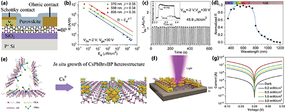
Figure 21. (a) Schematic illustration of Schottky barrier-controlled CH3NH3PbI3−x Clx /few-layer BP phototransistor. (b) Responsivity of the device at different illumination intensity. (c) Temporal photocurrent response of the device. (d) Wavelength dependent responsivity of the photo FET. [180] John Wiley & Sons. [© 2019 WILEY‐VCH Verlag GmbH & Co. KGaA, Weinheim]. (e) Schematic of in-situ synthesis of the CsPbBr3 NCs/BP NSs heterostructure. (f) Schematic configuration of CsPbBr3/BP PD. (g) I–V characteristics of the device at different illumination intensity. Reproduced from [181] with permission of The Royal Society of Chemistry.
Download figure:
Standard image High-resolution imageChen and co-workers synthesized of all inorganic CsPbBr3 NCs/BP NSs heterostructures (figure 21(e)) via a in situ hot-injection method for photodetection [181]. Due to the strong bonding between CsPbBr3 NCs and BP NSs, photogenerated carriers were separated and transferred efficiently, which yielded good the performance of the device. The device architecture is presented in figure 21(f), while figure 21(g) shows I–V characteristics of the PD in the dark and under the illumination at different light intensities. The device exhibits responsivity of 357.2 mA W−1 and detectivity of 2.62 × 10¹¹ Jones of under light intensity of 0.2 mWcm−2.
2.4. Perovskite/MXene photodetector
A new class of 2D transition metal carbides, carbonitrides and nitrides, named MXenes, has emerged as a potential candidate for optoelectronics [182–184]. MXenes serve various roles in PDs, such as photo absorbers, transparent electrodes, Schottky contacts, and plasmonic materials [182]. Deng and co-workers reported CsPbBr3 NSs/conductive Ti3C2Tx MXene flexible PD for photo communication, as illustrated in figure 22(a) [185]. Under illumination, electron and hole pairs were generated in the perovskite layer and transferred to MXene electrodes (figure 22(b)). The temporal photoresponse of the PD with different thicknesses of the MXene electrode under 450 nm light illumination at a bias of 10 V is presented in figure 22(c). The device exhibits photoresponsivity of 44.9 mA W−1, detectivity of 6.4 × 10⁸ Jones, and a maximum on/off ratio of 2.3 × 10³. Photocurrent growth and decay times were measured to be 48 and 18 ms, respectively (figure 22(d)). The PD maintains the excellent flexibility and stability after 1500 bending cycles.
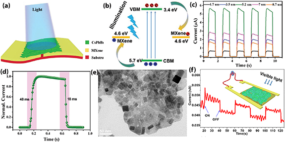
Figure 22. (a) Schematic of CsPbBr3/MXene flexible PD. (b) Energy level diagram of perovskite/MXene PD showing photogenerated carrier transfer. (c) Temporal photocurrent of the devices with different thicknesses of MXene electrodes. (d) Temporal photoresponse showing rise and fall times. [185] John Wiley & Sons. [© 2019 WILEY‐VCH Verlag GmbH & Co. KGaA, Weinheim]. (e) TEM image of CsPbBr3/MXene nanocomposite. (f) Temporal photocurrent response of devices based on CsPbBr3 NCs/MXene. Reprinted with permission from [186]. Copyright (2019) American Chemical Society.
Download figure:
Standard image High-resolution image
Pan et al reported visible light and x-ray PD based on CsPbBr3 NCs/Ti3C2Tx MXenes nanocomposite [186]. 2D MXene NSs were synthesized through the conventional acid etching and delamination of Ti3AlC2. Perovskite NCs were grown on MXene NSs. Figure 22(e) depicts the TEM image of the nanocomposite. The temporal photoresponse of the PD is shown in figure 22(f), while the inset of the figure shows the schematic of the device. However, the on/off ratio and responsivity of the device were very low.
3. Conclusions and outlook
Herein, we have systematically reviewed the recent developments in metal halide perovskite/2D materials hybrid PDs. Due to their unique optical properties, high carrier mobility, and superior mechanical flexibility, atomically thin 2D materials have been widely investigated in PDs, which show a very fast photoresponse speed along with high responsivity. However, the performances of these 2D material based PD are restricted by the low light-harvesting capability of monolayer and few-layer material. On the other hand, halide perovskite has an excellent capability of light-harvesting with a large absorption coefficient. Thus, the integration of 2D TMD materials with high light-harvesting perovskite materials could lead to considerable enhancement in the light absorption and result in high responsivity along with fast photoresponse due to high carrier mobility in 2D TMDs. In the reported PDs, halide perovskites serve as a light-harvesting active layer, while ultra-thin 2D materials serve various roles, such as charge transport layer/channel, Schottky contacts, photo absorbers, etc. Among the reported perovskite/graphene PDs, most of the reports are on perovskite/graphene-based phototransistors and Schottky junctions PDs due to the metallic behavior of graphene with zero bandgap. In this type of photo FET, perovskite absorbs the incident light, and graphene acts as a carrier transporting channel material. These photo FET working on the strong photogating effect can exhibit very high photoresponsivity (109 A W−1). Zero-dimensional perovskite QDs/NCs-graphene-based photo FETs also have been reported. Compared to organic–inorganic hybrid perovskite, all-inorganic perovskite NCs/QDs shows enhanced ambient stability. All inorganic perovskite NCs/graphene photo FET exhibits a responsivity as high as 8.2 × 10⁸ A W−1 and detectivity of 2.4 × 10¹⁶ Jones. 2D perovskite/graphene photo FET and photo FET on flexible substrates are also reported, which shows excellent stability and flexible durability, respectively. TiO2/graphene/perovskite self-powered PD can work without any applied bias with the responsivity of 0.375 A W−1. The photoresponse speed of the self-powered PD was faster (∼5 ms) than the other reported perovskite/graphene based photo FETs.
Among the reported perovskite/2D TMDs based PDs, most of the reports are on perovskite/MoS2 photo FET and type-II heterojunction PDs. The maximum responsivity of perovskite/MoS2 photo FET has achieved ∼104 A W−1, while the maximum responsivity was observed about 1013 Jones. Perovskite film, QDs or NCs/monolayer MoS2 type-II heterostructure PDs can detect light without external bias due to the built-in potential across the heterojunction. The photoresponsivity of 2D perovskite/MoS2 self-powered hybrid PD was reported of 0.12 A W−1. CsPbBr3 NCs/monolayer MoS2 type-II vertical heterojunction PD showed very fast photoresponse of few μs. WS2 and WSe2 based perovskite PDs exhibit maximum photoresponsivity of 679 and 1.1 × 10²A W−1, respectively. The maximum specific detectivity of WS2 and WSe2 based perovskite PDs was observed about 1014 and 1011 Jones, respectively. Newly discovered PdSe2 and PtSe2 are a promising member of the TMDs family with semi-metallic properties. Perovskite–PdSe2 and PtSe2 based self-powered hybrid PDs show very fast photoresponse (∼10−8 s). Other 2D materials such as BP, MXene–perovskite PDs have also been reported with inferior performance, and thus needs further exploration.
Despite the remarkable progress in this field of perovskite/2D material PD, there are many unresolved issues and challenges that need to be addressed, and there are plenty of room for further improvement towards commercial applications of perovskite/2D material based devices. Few major issues related to perovskite optoelectronic devices are: (a) poor ambient stability in the presence of oxygen and water molecules, (b) ion migration resulting poor storage stability of the devices (c) toxicity of lead, (d) reproducible methods of device fabrication. Though perovskite optoelectronic devices show excellent performances, perovskite-based devices usually degrade when they are exposed to thermal-stress, light, electric fields, oxygen, or moisture. Compared to organic–inorganic hybrid perovskite, all inorganic and 2D halide perovskite show enhanced ambient stability. Thus, future studies would be required for stability improvement. The thermal energy and local polarization can generate fast and slow ion migration in perovskite semiconductors. By grain boundary passivation, fast ion migration in perovskite such as the migration of iodine defects can be suppressed, whereas the slow ion migration is still an important issue that hinders the low-term stability of the device. Further investigation would be required to gain deeper insights into degradation and ion migration in metal halide perovskites/2D material based PDs. There have been some successful strategies to improve the stability of solar cells. However, such studies are lacking for perovskite based PDs. The toxicity of lead on humans and the environment has been a challenge for the development and commercialization of perovskite-based PDs. However, lead-free perovskite (including tin, copper, and germanium etc based) possesses poor ambient and storage stability compared to lead-based perovskites. Thus, further investigation is required on lead-free perovskite/2D material based PDs. Among the reported perovskite/2D material PDs, in most of the reports, perovskite films/nanostructures were fabricated by solution-processable technique. However, reproducibility and large scale fabrication for commercial applications are the major issues by this technique. Thus, alternative fabrication method of perovskite films/nanostructures should be explored.
The perovskite 2D material interface plays an important role in device performance. The trap states present at the interface can lead to poorer photodetection performance. The passivation of trap steps by different physical and chemical methods can substantially enhance the performance of the devices. For synthesis of perovskite nanostructures, different surfactants are used. Residue of this surfactant can result in slow photoresponse speed. Thus, investigation of alternative synthesis and processing method of high quality perovskite nanostructures should be required. The performance of the perovskite/2D material PDs can also be further improved by the engineering of device structure and interface layers. The integration of perovskite with different newer 2D materials should be explored for photodetection. The spectral photoresponsivity of perovskite/2D material PDs are limited to UV–visible region. However, development of NIR PDs using perovskite/2D material heterostructure is very important for different technological interests. The spectral response range of PDs can be extended by utilizing mixed-halide perovskite materials with smaller optical bandgap and by combining up-conversion materials with perovskite materials. Thus, further investigation would be required on perovskite/2D material PDs for NIR photodetection. Flexible PDs own extensive research attention in the field of wearable and portable devices. Further investigation is required on perovskite/2D material flexible PD. Plasmonic nanostructures at perovskite/2D material interface can help in superior light-harvesting of the PDs. Further studies are required on the fabrication of perovskite/2D material vertical heterojunction self-powered PDs.
There has been a lot of recent interest in the synthesis of 2D perovskites for various optoelectronic applications. The term 2D refers to the intrinsic 2D crystal structures of Ruddlesden–Popper perovskites or perovskite NSs and nanoplates with ultralow thickness. Recent studies have demonstrated the feasibility of constructing heterostructures of 2D perovskites with other 2D-layered materials [187, 188]. It would be interesting to explore the integration of 2D perovskites with other inorganic or organic semiconductors and functional oxide perovskites for PD applications [189]. Single crystal perovskite nanostructures shows interesting polaron physics and exciton–photon coupling that could be explored for heterostructure PD applications. Thus, perovskite/2D material based hybrid PDs are just emerging and require more knowledge on properties, device optimization for different technological interest. We expect that this review will stimulate more dedicated investigations of this emerging field for commercialization and practical applications of the hybrid devices.
Acknowledgments
We acknowledge the financial support from MEITY (Grant No. 5(9)/2012-NANO(VOL-II)) for carrying out part of this work.
Data availability statement
All data that support the findings of this study are included within the article (and any supplementary files).