

Abstract
Although optical 3D topography measurement instruments are widespread, measured profiles suffer from systematic deviations occurring due to the wave characteristics of light. These deviations can be analyzed by numerical simulations. We present a 3D modeling of the image formation of confocal microscopes. For this, the light-surface interaction is simulated using two different rigorous methods, the finite element method and the rigorous coupled-wave analysis. The image formation in the confocal microscope is simulated using a Fourier optics approach. The model provides high accuracy and advantages with respect to the computational effort as a full 3D model is applied to 2D structures and the lateral scanning process of the confocal microscope is considered without repeating the time consuming rigorous simulation of the scattering process. The accuracy of the model is proved considering different deterministic surface structures, which usually cause strong systematic deviations in measurement results. Further, the influences of apodization and a finite pinhole size are demonstrated.
Export citation and abstract BibTeX RIS

Original content from this work may be used under the terms of the Creative Commons Attribution 4.0 license. Any further distribution of this work must maintain attribution to the author(s) and the title of the work, journal citation and DOI.
1. Introduction
Since the size of electrical and optical components is continuously decreasing, the demand for accurate measurement technology increases in order to ensure high quality. Thus, the development of appropriate measurement technology is a large field of research [1–8]. Optical profiling techniques such as coherence scanning interferometry (CSI) and confocal scanning microscopy (CSM) are widespread for fast and contactless topography measurements on the micro- and nanoscale. Due to a superior lateral resolution compared to CSI and further an enhanced axial as well as lateral resolution in contrast to conventional microscopes, CSM is often applied if high accuracy is demanded. Compared to tactile measurement instruments and scanning probe microscopes, CSI and CSM are faster and contactless. Such optical sensors providing high axial and lateral resolution are for example needed for nanopositioning and nanomeasuring technology [9, 10] or measurements of surface properties of silica waveguides such as surface roughness [5] and side wall angles [6].
As light interacts with the measurement object, optical profilers suffer from diffraction, obscuration and material as well as shape dependent reflection properties leading to systematic deviations between measured and real topographies [4, 11–15], which vary between different profiler setups. In order to reduce these deviations on the one hand and to find the most reliable measurement instrument with regard to specific applications on the other hand, analytical and numerical models are applied.
In former studies various models are developed for conventional microscopy [16–18], CSI [4, 19–23] and CSM [4, 12, 14, 17, 20, 24–28] on the basis of analytical approximations [4, 12, 14, 20, 21, 24–28] as well as based on rigorous numerical models [16–19, 22, 23]. In general, rigorous models show better agreement with measurement results, whereas analytical approximations provide better insights in the physical mechanisms of the measurement process and require less computational effort. Furthermore, de Groot et al [29] applied the model developed by Totzeck [16] in a model-based CSI system.
Although CSI provides an outstanding axial resolution, which is almost independent of the numerical aperture (NA) of the objective lenses, CSI supplies less lateral resolution than CSM. Additionally, the phase detection in CSI in particular close to the lateral resolution limit requires an appropriate choice of evaluation parameters [8]. Further, CSI is known for distinct systematic deviations at edges and steep slopes caused by the superposition of fringes in depth responses within the lateral resolution [4, 13]. However, systematic deviations with regard to edges and slopes are also observed in CSM [4, 6, 12]. In addition, CSM uses (partially) spatially coherent illumination, whereby interference effects in the scattering process of the incident beam with the measurement object are enhanced. For these reasons a numerical model enabling a comparison of the accuracy of optical profilers with respect to certain surface profiles without the need for performing measurements is of high interest for manufactures, scientists and industry.
In order to develop a model, which enables to compare various optical measurement instruments reliably with respect to the accuracy for versatile measurement objects, we extend the rigorous CSI model introduced in [23, 30] to CSM. Compared to former studies modeling CSM our model provides a full lateral scan without repeating the time-consuming rigorous simulation for each point on the measurement object. Thus, if the light-surface interaction is simulated rigorously once, the simulation of the measurement process can be performed and the accuracy can be compared for different measurement instruments. In order to underline the reliability of our model, we show reconstructed surface topographies obtained by simulations and compare them to measurement results. In this context, the influences of varying pupil functions and a finite pinhole size are discussed with respect to measurement objects providing large spatial frequencies. Additionally, an atomic force microscope (AFM) measurement result is used as input surface topography for rigorous simulations. Both, confocal as well as AFM measurement results are obtained by a multisensor measuring system [31, 32].
2. Model
A schematic representation of a standard CSM is given in figure 1(a). In this microscope setup the same pinhole disk is used for illumination and imaging. Thus, one point of the pinhole is imaged to the measurement object and the illuminated spot is imaged back to the relating pixel of the camera. The model is split in three parts, the illumination, the rigorous simulation of the light-surface interaction and the imaging process. The pinhole disk is assumed to be infinitely small in the derivation of the model, whereas a finite sized pinhole is considered by additional filter functions. Further, the microscope is assumed to be perfectly adjusted. However, aberrations could be applied in the model analogously to the work of Rahlves et al [14].
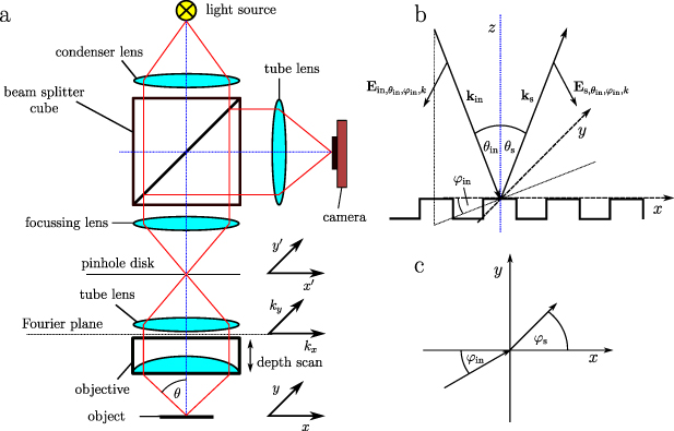
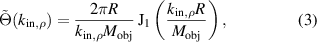
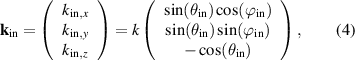
Figure 1. (a) Schematic representation of a confocal microscope. (b) Sketch of the scattering geometry including the definition of the incident and scattered angles. (c) Incident and scattered angle in the xy-plane.
Download figure:
Standard image High-resolution image2.1. Illumination
As the light source is imaged to a pinhole disk (see figure 1(a)) with an infinitesimal small pinhole at the position  , the illuminating electric field
  immediately behind the pinhole can be written as:

with the electric field  above the pinhole determining the amplitude and the polarization. The subscript '
 ' is used to denote the incident field, '
 ' clarifies the field close to the pinhole. The electric field beyond the pinhole is then transferred to the Fourier plane by a tube lens (see figure 1(a)) leading to a plane wave:

where  denotes the Fourier transform of
  depending on the spatial frequency components
  and
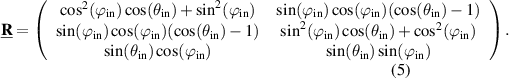
and  . Having regard to a finite pinhole size, the pinhole can be considered by the convolution of the δ-functions in (1) with the shape of the pinhole. Thus, assuming a circular pinhole of radius R, (2) is multiplied by a rotationally symmetric filter:
where J1(·) is the Bessel function of first kind and order,  the magnification of the microscope objective and
  is the radial amount of the wave vector. In case of surface structures, which are invariant under translation in one direction,
  can be integrated numerically along this direction. Note that the result of this integration is not described by a sinc-function analogously to the coherent line spread function in [25] due to the limited NA. Overall, the consideration of a finite pinhole size is treated analogously to Sheppard et al [33], whereby we assumed spatially coherent pinhole illumination for simplicity. Therefore, an enveloped plane wave hits the back focal plane of the objective and is focused onto the measurement object with regard to the position in lateral
  -space. The wave vector
  of the incident wave is given by:
where  defines the angle of incidence with regard to the optical axis,
  the azimuth angle in the xy-plane and k = 2π/λ the wave number including the wavelength λ. Note that the optical axis points upwards. A schematic representation of the angles of incidence is given in figures 1(b) and (c). As the electric field is still perpendicular to
  , the polarization of the incident field above the objective is even rotated with regard to the position above the objective and, thus, with respect to the angles of incidence. The electric field incident on the object is rotated by the matrix [16, 23]:
Hence, the electric field at the point  for a monochromatic incident wave is given by:
The maximum angle of incidence is restricted by the NA of the objective lens  . The sine and cosine functions follow from the circular objective lens and the substitution
  with the radial component
  of the wave vector in cylindrical coordinates and
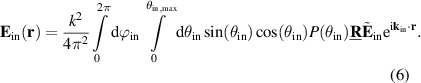
  is the pupil function considering apodization. In contrast to CSI modeling, where the intensity is integrated [23], here the angular integration is performed over the electric field as the illumination is partially coherent due to the pinhole [25]. Taking into account polychromatic illumination, the total intensity can be calculated by integrating over the intensities obtained for each wave number in the spectrum. Since the scattering process and the image formation are computed before the intensities are determined, polychromatic illumination is taken into account within the image formation.
2.2. Light-surface interaction
The light-surface interaction sketched in figure 1(b) is calculated rigorously by two different methods, finite element method (FEM) and rigorous coupled-wave analysis (RCWA). In both cases the scattering of plane incident waves of the form:

at the surface topography is simulated and the far-field of the scattered field is computed. Thus, there are two possibilities to discretize the simulation. On the one hand, the angles of incidence in the integrals given in (6) can be discretized and the rigorous simulation is repeated for each discrete pair of angles. In this case the phase factor according to the pinhole position  ,
, , which corresponds to the lateral scan, only depends on the incident angles and the pinhole position (see (2)) and, thus, can be multiplied to the scattered fields after the rigorous simulation. On the other hand, the integral could be computed in parts analytically and other components numerically before the rigorous simulation. In this case the simulation needs to be repeated for each position (
 ,
, ) of the pinhole. Both options show advantages over the other depending on given parameters. In this study we focus on the first possibility in order to be in correspondence with former studies of other optical profilers. Thus, since the scattering process is computed once, the resulting far-fields could be used to analyze the transfer behavior of various optical measurement instruments. Note that the pupil function
  in (6) only depends on
  and, thus, can be considered in the image formation as well.
Due to a significant saving of computation time and memory demand, we focus on 2D surface structures which are invariant under translation in one direction (here y-direction). Therefore, the scattering problem is solved for a section out of the 3D surface structure at a fixed y-position (here y = 0), whereas oblique angles of incidence are still considered and, thus, the exact solution is provided. As one point ( ) just illuminates the corresponding (spread) point (
 ) on the surface and inversely the light scattered at the point (
 ) only contributes to the pixel related to
  ,
,  follows.
The FEM model used in this study is explained in detail in [23]. The open source FEM solver 'NGSolve' [34] is applied to solve the occurring boundary value problem. The commercial solver 'Unigit' [35] is used to solve the scattering problem using RCWA as described in [36–38], where N = ±80 Fourier coefficients are taken into account. Since the lateral scanning process, which is described by the exponential function in (2), does not depend on the object coordinates x, y, z, this term does not have an impact on the scattering process. Therefore, the light-surface interaction is computed once for each discrete set of incident angles and multiplied by the exponential term afterwards for each pixel of the camera. The resulting far-fields are taken in order to simulate the image formation in the microscope.
2.3. Image formation
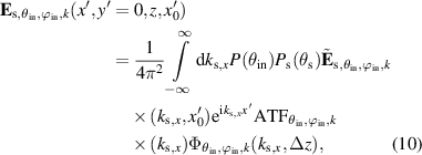
The rigorous simulation models provide the far-fields  for each set of incident angles. The subscript 's' marks the scattered field and
  ,
,  denote the spatial frequency coordinates of the scattered field and, thus, the wave vector components corresponding to the scattering angles
  and
and  (cp figures 1(b) and (c)). Note that the phase factor according to the pinhole position
  is multiplied to the computed far-fields for each position of the pinhole (see (2)). Since we consider 2D surface topographies,
  and hence the axial wave vector component
  is given by
  . In order to find the focal position of each point on the measurement object, a vertical scan is performed with the objective lens (see figure 1(a)). Thus, the phase shift,

depending on the shift Δz = z0 − z in vertical (z-) direction with the reference position z0 of the far-fields (cp [23, 30]) is caused by the depth scan. Further, the scattered light field is multiplied by the coherent amplitude transfer function:
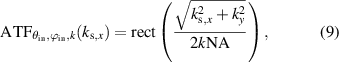
of the objective lens, as waves including large spatial frequencies with regard to the lateral direction are not imaged. According to the depth scan and the transfer behavior of the objective lens, the scattered electric field in the pinhole plane for one incident plane wave is given by the inverse Fourier transform:
where  is the pupil function contributing to the scattered field due to apodization. Note that the pupil functions affecting the incident and the scattered field differ in case of inhomogeneous illumination, which is included in
  . Since both,
  as well as
  , act as low-pass filter of the signals, we only analyze the influence of
  in this study and thus,
  is chosen for simplification.
Considering monochromatic coherent conical illumination (see (6)) the total scattered electric field:
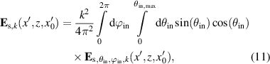
is derived by integrating the electric field over the angles of incidence. Therefore, the intensity:

is proportional to the absolute square of the electric field at the position  as the pinhole disk blocks light propagating from other positions in
  space. Considering a finite pinhole size, the intensity is integrated over the area of the pinhole around
  . With regard to polychromatic light sources with the spectral distribution S(k) the total intensity is given by integration over the intensities obtained for each monochromatic wave as follows:
The intensities obtained by simulations according to (13) and measurement results are analyzed by a Gaussian fit. Thereby, the threshold value of the fitting-area is set to 0.6 of the maximum value.
3. Results
In the first part of this section, two rectangular gratings of the Simetrics RS-N resolution standard [39] with period lengths of L = 6 µm and L = 400 nm are simulated using FEM as well as RCWA and compared to measurement results. The nominal step heights amount h = 190 nm and h = 140 nm, respectively.
The second part of this section contains simulation and measurement results of a chirp standard [32] manufactured by the PTB (Physikalisch-Technische Bundesanstalt, Germany) including steep slopes. Thus, the high lateral resolution capability of confocal microscopes is demonstrated. In order to achieve a more realistic simulation, an AFM measurement result of the chirp standard is used as the scattering surface. Further, the influence of different pupil functions, which describe apodization effects as well as the pupil illumination, and the influence of a finite pinhole size are discussed for both, the RS-N as well as chirp standard. Finally, simulation results of a surface structure with cylindrical trenches including slopes close to the theoretical limit given by the objective lens are shown.
The confocal microscope (Nanofocus µ surf) uses an unpolarized spatially extended cyan LED with a central wavelength of  nm and a spectral bandwidth defined by the full width at half maximum of 35 nm. The NA of the microscope comprises 0.95, the magnification
  of the objective lens amounts 100, the magnification
  of the entire imaging system is approx. 45 and the pixel width of the camera is given by
  m. The repeatability and uncertainty of the CSM as well as the AFM were studied in detail by Hagemeier and Lehmann [40]. The AFM was laterally calibrated using a BudgetSensors HS-100MG calibration standard [41]. Since the uncertainty of our measurement instruments is in the range of 1 nm and the observed deviations are in the range of 10 nm and larger, they can be identified as systematic deviations. As we are mainly interested in systematic deviations occurring at deterministic surface structures and the measurement objects are not superimposed by additional roughness, roughness effects are not considered in this paper. Further, measurements were repeated with very similar results. Therefore, just one of the measurement results is shown, respectively.
3.1. Rectangular grating
Figure 2 shows simulation and measurement results of the Simetrics RS-N resolution standard with a period length of L = 6 µm and a nominal height of h = 190 nm. The material of the RS-N is silicon and, thus, the refractive index of  is assumed [42]. As the spectral width of the light source is relatively small and the refractive index does not change significantly over this range, the refractive index is assumed to be constant within the bandwidth of the light source. The upper figures 2(a)–(c) show the intensity signals simulated with FEM (figure 2(a)) as well as RCWA (figure 2(b)) and measured (figure 2(c)) depending on the x-coordinate. The intensities are normalized by its maximum value, respectively. In the simulations, the pupil function is set to
  constituting the case of a homogeneously illuminated objective pupil without apodization effects and the pinhole is approximated to be infinitely small. Comparing simulation and measurement results, the depth of field in the measurement result is slightly larger than in the simulation. This discrepancy follows from the approximations of an infinitely small pinhole and homogeneous illumination mentioned above as it will be demonstrated later in this section. Despite this discrepancy, measurement and simulation show in general good agreement. The grating structure can be obtained clearly in the focal peaks in all of the three figures. At the edges of the grating the course of the maximum intensity seems to be undefined due to interference, obscuration and diffraction effects in all three figures. In order to analyze the behavior of the signals at the edge of the grating in detail, cross sections of the intensity signals at certain x-positions are regarded in the following.

Figure 2. Simulation and measurement results of the L = 6 µm Simetrics RS-N resolution standard. The upper row of figures (a)–(c) shows normalized confocal response signals depending on the x-coordinate obtained by simulation using FEM (a) as well as RCWA (b) and measurement (c). The middle row (d)–(f) shows cross sections at defined lateral (x-)values from an upper plateau (blue), a lower plateau (red) and an edge (green), respectively. The corresponding evaluated grating structures are displayed below in (g)–(i). The pixels relating to the signals in (f) are marked by dashed colored lines in (c) and points in (i).
Download figure:
Standard image High-resolution imageFigures 2(d)–(f) display cross sections of the depth signals above obtained at the upper, the lower plateau and the edge as marked by the dashed lines in the measurement result (see figure 2(c)). In the simulation results the respective pixels are not highlighted by dashed lines as additional simulations with pixels placed exactly at the corresponding grating position are performed in order to obtain the signals. In all of the figures the maximum intensity received from the upper plateau is slightly larger compared to the maximum intensity obtained at the lower plateau according to obscuration. Regarding the side lobes, the signals of the upper and lower plateaus show asymmetry depending on the corresponding plateau, which seems to be mirrored at the intensity axis. It should be noted that the height of the side lobes can be influenced by the pupil function and can be adjusted by choosing:

as described by Sheppard and Larkin [43]. Note that η = 0 represents the case of a homogeneously illuminated pupil plane according to [43], where  since the factor
  following from substitution is included in the pupil function in [43]. The influence of the pupil function on signals and results will be demonstrated later in this section.
The signals received at an edge of the grating are presented by green lines. In simulation as well as in measurement results the amplitude of the signals is significantly decreased due to diffraction effects and the transfer behavior of the microscope with regard to high frequency components, which occur at steep edges. The simulation results show good agreement, whereas the measurement result seems to be slightly shifted to higher z-values. However, it should be noted that in practice the pixel is not exactly located over the edge, as it is possible in simulations. For clarification, the pixels related to the signals in figure 2(f) are marked by points in the resulting grating depicted in figure 2(i). Further, the edges of the RS-N standard in reality are not perfectly perpendicular as demonstrated by AFM measurement results in [23]. Thus, the signals obtained by both simulations and measurement show in general good agreement.
Figures 2(g)–(i) display resulting grating structures corresponding to the signals presented above. Both, simulation and measurement results show an amplitude of  nm, which is larger compared to the prescribed height of h = 190 nm in simulation and in reality as confirmed by AFM results in [23]. Probably, this deviation follows from diffraction effects caused by the interaction of light with the grating structure and a superposition of decaying overshoots from adjacent edges, due to periodicity. The slight asymmetry of the gratings emerges from the arrangement of the pixels over the surface structure and can be observed in all three results. Further, the gratings show overshoots on the edges, whereby in case of both simulations (figures 2(g) and (h)) the overshoot is larger compared to the measurement (figure 2(i)). The overshoots follow from a superposition of reflected waves from the upper and lower plateau, which both contribute to one pixel due to the optical resolution of the objective. It should be noted, that the real grating structure does not exhibit exactly perpendicular edges [23], but since the width of the edges is smaller than the resolution limit of the microscope the edges can be treated as perpendicular. The simulated and measured edges do not seem to be exactly perpendicular in the reconstructed grating, which is caused by the pixel width. Considering the magnification of the microscope and the pixel pitch of the camera a lateral sampling interval of 160 nm results between two measured grating points. Thus, the grating does not seem to be perpendicular, although the jump between two plateaus is usually performed from one pixel to the next.
Small deviations between FEM and RCWA results probably follow from Gibbs phenomenon [44], which affects the RCWA in case of vertical and almost vertical edges, due to the Fourier series expansion included in the model. Thus, the grating cannot be reproduced exactly leading to deviations. Furthermore, the RCWA suffers from a convergence problem for TM polarized light in case of highly reflective surfaces as analyzed by Li and Granet [45, 46], what leads to additional deviations between both models. In case of FEM the surface is discretized by triangles, and hence, FEM is well suited for vertical edges and highly reflective material with the drawback of an increasing computational effort. However, apart from slight deviation, which are expected using two totally different simulation models, FEM and RCWA show good agreement. In order to investigate the influence of apodization and a finite sized pinhole and to improve the agreement between measurement and simulation, signals and reconstructed gratings resulting from FEM simulations will be compared for various pupil functions and an infinite and finite sized pinhole in the following.
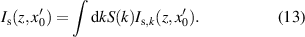
To underline the influence of the pupil function on the signals, figure 3(a) presents signals from the upper plateau simulated with FEM for different values of η, where every signal is normalized by its maximum value. Comparing the results for different pupil functions, the modulation of the side lobes is damped with increasing value of η. Therefore, differences in the occurrence of the side lobes between simulation and measurement probably follow from apodization effects and an inhomogeneous aperture illumination of the objective lens, which is expressed by the pupil function. As expected, the width of the signals slightly increases with increasing value of η since high angles of incidence are damped and thus, the effective NA is reduced. These observations are in good agreement to analytic and measurement results presented by Fewer et al [47]. Compared to the measurement result in figure 2(c), the curve for η = 1/2 seems to show the best agreement. The corresponding reconstructed grating structures are displayed in figure 3(b). With increasing values of η the overshoots become sharper with regard to the lateral axis and the amplitude of the reconstructed structures marginally decreases. Caused by sharper overshoots, the finite size of the pinhole should be considered operating as an additional low-pass filter since sharp overshoots include large spatial frequencies. Figure 3(c) depicts grating structures for η = 1/2 considering a pinhole of radius R = 15 µm , which is estimated regarding a microscopic image of the pinhole disk. The unfiltered orange curve corresponds to the orange one in figure 3(b). As presumed above, the overshoots are damped by the pinhole size acting as a low-pass filter. The resulting grating structure shows good agreement with the measurement result regarding the amplitude of the grating, the asymmetry of the overshoots, a marginally upward overshoot and a larger downward one. Small deviation in the height of the downward overshoot can be explained with the shape of the measured object, which does not exactly comply with a rectangular grating as shown by Pahl et al [23], and by small misalignments that are inevitable in real measurements. In sum, the signals as well as the resulting rectangular grating structure can be predicted reliably by the FEM simulation. Further, the size of the pinhole and the pupil function play an important role for rectangular grating structures, as high spatial frequencies contribute to the signals.
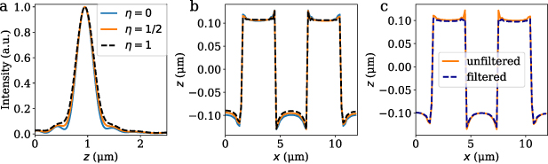
Figure 3. FEM simulation of the L = 6 µm Simetrics RS-N resolution standard for different pupil functions and considering a finite sized pinhole. (a) Signals resulting from an upper plateau for different values of η in (14). (b) Corresponding evaluated grating structures. (c) Evaluated grating structures for an infinitely small pinhole and filtered by a pinhole of R = 15 µm with η = 1/2.
Download figure:
Standard image High-resolution imageFurther systematic deviations such as an decrease of the measured amplitude are expected if structures with period lengths closer to the lateral resolution limit are considered [8]. Figure 4 displays reconstructed rectangular grating surfaces of the RS-N standard with L = 400 nm and h = 140 nm. The red lines show simulated (figures 4(a) and (b)) and measured (figure 4(c)) results with a camera pixel width of  m . Figure 4(d) presents the same measurement result of figure 4(c) over a larger x-range, in order to demonstrate that the measured amplitude of the grating is continuous. In general, the shape of the lines show good agreement in all three figures. It should be noted, that the pixels in case of the measured result are not exactly at the same position as the positions chosen for the simulations leading to an asymmetry in the measurement result. Further, the amplitude is significantly decreased compared to the nominal height of h = 140 nm in all three cases, due to the transfer characteristics of microscopes with regard to high spatial frequencies [8]. Comparing figures 4(a) and (b), the amplitude (peak-to-valley) of the RCWA result is approx. 1.5 nm larger than the amplitude of the FEM result. This small deviation probably follow from the disadvantages of the RCWA mentioned above and the fact that two models based on completely different approaches are used. The simulated amplitudes show good agreement to the measurement result (figure 4(c)), whereby it should be noted that the measured amplitude differs from pixel to pixel and measurement to measurement in a range of approx 5 nm. Thus, it is hard to say if RCWA or FEM show better agreement. Additionally, small deviations in the amplitude could be aligned by considering a finite pinhole size and an appropriate pupil function as shown above. Furthermore, the grating is assumed to be an ideal rectangular grating, which slightly differs from the AFM measurement result shown in figure 4(e). However, despite small deviations, simulation and measurement results show good agreement and the strong decline in the measured amplitude can be seen clearly in both. The blue lines in figures 4(a) and (b) show the results assuming a smaller pixel width of
  m in order to demonstrate that the structure is still resolved, what is hard to see in the measurement result by reason of the large pixel size. As expected, the simulated results show a sinusoidal course with the period length of L = 400 nm. Considering small period lengths close to the resolution limit only the first positive and negative diffraction orders of the scattered field contribute to the imaging by the objective lens leading to a mono-frequent phase object (PO) resulting in a sinusoidal shaped result. Small deviations from an ideal sinus follow from diffraction effects and broadening of the diffraction orders according to a broadband light source. In sum, the significant decrease of the amplitude can be observed in measurement as well as both simulation results. Figure 4(e) shows the nominal grating structure applied in the simulations, an AFM measurement result and the FEM simulation result of figure 4(a). The AFM result is obtained using an high density carbon electron beam deposited—high aspect ratio cantilever described in [32] and proved by repeated measurements in [40]. Taking the AFM result as reference the height of the real grating is slightly larger than the nominal height and the edges are not totally vertical, but nonetheless they can be treated as perpendicular due to the resolution of the microscope. Since we are interested in systematic deviations occurring at determined structures, considering the ideal grating in the simulation is sufficient in this section. Comparing the nominal height of the grating to the FEM result, the significant decrease of the amplitude in the FEM simulation and due to the agreement to the measurement result (see figures 4(c) and (d)) also in the measured amplitude is observed.
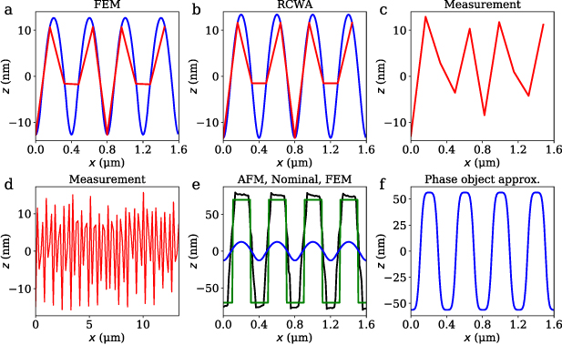
Figure 4. Results of the L = 0.4 µm Simetrics RS-N resolution standard simulated assuming an infinitely small pinhole and measured. The results for the used camera pixel width of  m are marked by red lines simulated with FEM (a), RCWA (b) and measured (c). The blue lines in (a), (b) and (f) indicate the results supposing a pixel width of
  m , where (f) is simulated approximating the measurement object as a phase object [4]. In (d) the measurement result shown in (c) is displayed over a larger area. (e) Nominal structure supposed in the simulations (green), the structure measured by AFM (black) and the FEM simulation result (blue) according to the blue line in (a).
Download figure:
Standard image High-resolution imageFigure 4(f) shows a reconstructed grating structure simulated using the PO approach known from Fourier optics [4], instead of a rigorous simulation model. In the PO approach the object only influences the phase of the reflected wave and, therefore, obscuration, multiple scattering effects and polarization dependent diffraction effects are neglected. The amplitude obtained by the PO better corresponds to the nominal amplitude of the grating and is only reduced by approx. 30 nm. Thus, the PO result differs from rigorous and measured results. According to that, the decrease in the amplitude can not be simply explained by the transfer characteristics of the microscope. Obviously, the scattering process strongly affects the measured results and thus rigorous methods have to be applied for a reliable reproduction of the measurement process. For further analysis the confocal depth signals are taken into account.
Figure 5 displays the depth response signals obtained by FEM (figure 5(a)), RCWA (figure 5(b)) and the PO approximation (figure 5(c)) corresponding to the reconstructed structures shown in figures 4(a), (b) and (f), respectively. Apart from small deviations, the FEM and the RCWA results show good agreement again. In the PO result the upper and lower plateaus of the grating structure can be seen clearly, whereby the course of the grating between to plateaus is blurred due to the limited optical resolution. In the rigorous simulation results no continuous course of the grating can be observed. Further, the amplitude from signals at the upper plateaus is significantly larger compared to the signals from bottom plateaus. This is a further indication, that obscuration of the edges and multiple scattering effects considerably influence the results. In case of the RS-N L = 400 nm structure, the nominal height of h = 140 nm is relatively large compared to the period length. Further, the confocal microscope provides a high NA leading to large angles of incidence. These properties of the measurement instrument and object probably enhance the obscuration and scattering effect significantly and thus, especially high NA imaging systems should be described by rigorous simulation methods.

Figure 5. Depth response signals of the RS-N standard with L = 400 nm and h = 140 nm simulated with FEM (a), RCWA (b) and the phase object approximation (c).
Download figure:
Standard image High-resolution imageApart from small deviations, both rigorous simulation models show good agreement for large and small period lengths. Since FEM shows the advantage of triangular discretization with the drawback of a significantly larger computation time, FEM is used in order to simulate results obtained by a chirp standard in the following.
3.2. Chirp standard
In order to analyze the transfer behavior of the confocal microscope with respect to steep slopes, figure 6 shows simulated and measured results of a PTB chirp standard. The material of the standard is nickel and, thus, a refractive index of  [42] is assumed in the simulations. Figure 6(c) displays an AFM measurement result of the chirp standard, where the area including the smallest period length and hence the largest spatial frequencies (see area between the red dashed lines) is extracted for the FEM simulation. In order to demonstrate that the chirp standard is almost invariant under translation in y-direction, figure 9(a) in the

Figure 6. Simulation and measurement results of the PTB chirp standard. (a) Simulated signals at a valley of the chirp (blue), at a slope (red), at the top (green) assuming an infinitely small pinhole as well as homogeneous illumination and measured signals at similar positions (b). The signals are normalized by the maximum of the signal obtained at the valley of the structure. (c) AFM measurement result of the chirp profile, where the area used for the FEM simulation is localized by red dashed lines. (d) Reconstructed simulated chirp structures for different pupil functions with η = 0 (blue), η = 1/2 (red) and η = 1 (green). (e) Reconstructed measured structure. The points in (d) and (e) mark the positions of the signals shown in (a) and (b) with the corresponding colors. The signals displayed in (a) belong to the blue structure presented in (d). (f) Reconstructed simulated structure for η = 1/2 assuming an infinitely small pinhole (red, solid) and a finite pinhole of radius R = 15 µm (darkblue, dashed). The red curve in (f) corresponds to the red curve in (d).
Download figure:
Standard image High-resolution imageFor the sake of completeness the full simulated and measured depth responses depending on the x-coordinate are given in figure 10 in the
Figure 6(d) depicts reconstructed surface profiles for different pupil functions (see (14)). As expected, the amplitude of the chirp structure decreases with higher values of η, since higher angles of incidence, which include higher spatial frequencies with respect to the lateral axis, are damped by the pupil function. Thus, the sharp upper plateaus are imaged with attenuated amplitudes compared to the bottom of the grooves, which show less steep flanks and are thus not effected by the limited optical resolution. The amplitude (peak to valley) of A ≈ 380 nm assuming η = 1/2 show the best agreement compared to the measurement result according to figure 6(e) with A ≈ 375 nm. Further, the amplitude of the simulated chirp structure is slightly decreased if a finite sized pinhole (see figure 6(f)) is considered. Therefore, the simulated height of structures including steep slopes strongly depends on the pupil function, which considers inhomogeneous illumination and apodization effects, and marginally depends on the pinhole size in case of small pinholes. As it will be shown in the following, the influence of the pinhole size is more significant in case of larger pinholes.
Hagemeier and Lehmann [40] demonstrate a decrease in the measured amplitude of the PTB chirp standard if a 50× objective is employed instead of the 100× used for measurement and simulation in the results shown above. In order to confirm this study, a 50× magnification is applied in the simulation leading to an increase of the relative pixel size of the camera and the relative radius of the pinhole. Simulated and measured results of the chirp standard using a 50× objective are shown in figure 7. Compared to results presented in figure 6, the amplitude of the reconstructed chirp standard is decreased in both, simulation and measurement. Thus, the effect observed in [40] can be generally confirmed by the simulation. Comparing simulation (figure 7(a)) and measurement results (figure 7(b)) the simulated structure for the estimated pinhole radius of R = 15 µm shows a slightly higher amplitude than the measurement result. Thus, the size of the pinhole is probably approached somewhat too small. Since the size of the pinhole is just roughly estimated, this seems to be the main reason for the slight deviations. Further, the amplitude of the signals significantly depends on the illumination and apodization as shown in figure 6(d). Additionally, small differences could be caused by misalignments in the microscope. However, the effect presented in [40] is confirmed by the simulation and besides inevitable deviations, due to approximated parameters, measurement and simulation show good agreement.

Figure 7. Simulated (a) and measured (b) results of the PTB chirp standard using a 50× objective. A finite sized pinhole of R = 15 µm and inhomogeneous illumination with η = 1/2 is assumed in the simulation.
Download figure:
Standard image High-resolution image3.3. Cylindrical groove
Finally, we study a concave cylindrical structure with a maximum sidewall angle of  corresponding to the maximum slope, which could theoretically be accepted by the CSM. Figure 8(a) sketches the geometry of the simulated structure, where the radius R and the size of the boundaries b are chosen to R = b = 1 µm . The period length of L = 3.9 µm is far away from Abbe's resolution limit and, thus the structure can be used to analyze the behavior of the CSM at surfaces with steep slopes. Further, we would expect to see an effect at the scan position, where the curvature of the wavefront corresponds to the curvature of the surface. In previous studies Mauch et al [12] presented a significant impact of this effect on the evaluated signals for smaller NA-values. Since we are interested in the occurring systematic deviations only, we use idealized parameters, i.e. the pupil function is set to one, the pixel width is chosen to be small and the pinhole is assumed to by infinitely small.
Figure 8. (a) Geometry and definitions of the simulated cylindrical structure with the radius R = 1 µm , the period length L = 3.9 µm , the flat boundary length b = 1 µm and the maximum slope angle of  . (b)–(d) Simulation result of the structure shown in (a) obtained by the CSM. Evaluated structure (b), corresponding depth signals (c) and cross sections of the depth signals at the steepest slope (
 ) and the bottom of the trench (
 ) (d). The x-positions of the cross sections are marked by dashed vertical lines in (b) and (c). The intensity at the maximum slope is depicted twice, once normalized by its maximum intensity (
 ) and once by the maximum intensity (
 ) of (
 ). The minor maximum in (
 ) marked by the dotted rectangle in (c) follows from the accordance of the wavefront's curvature with curvature of the cylinder in this point as explained by Mauch et al [12].
Download figure:
Standard image High-resolution image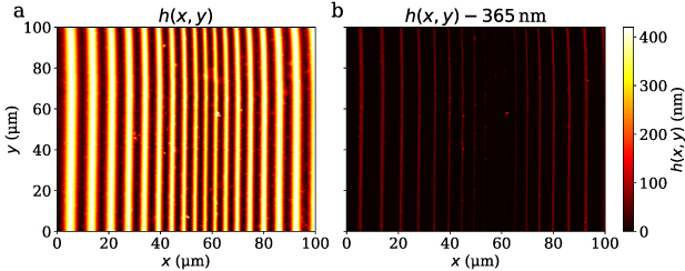
Figure 9. (a) AFM measurement result of the fine PTB chirp standard and (b) same result with height values reduced by 365 nm, which corresponds to the approximated height of the smallest period, where values smaller zero are set to zero for better visibility.
Download figure:
Standard image High-resolution image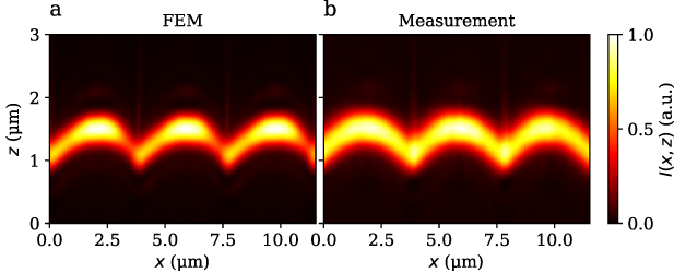
Figure 10. Normalized depth signals of the PTB chirp standard simulated with FEM (a) and measured by the CSM (b).
Download figure:
Standard image High-resolution image
Figure 8(b) displays the evaluated profile of the topography given in figure 8(a). At the steep slopes of the cylindrical structure, the results suffer from overshoots, whereby the upper one is larger than the downward one. Probably, the small upward overshoot is mainly caused by edge diffraction. The downward one follows from the loss of information at the steep slope and will be analyzed more detailed the following. The bottom of the cylindrical structure is reconstructed correctly. In this area we would have expected the wavefront effect discussed by Mauch et al [12]. In order to analyze the reasons for the downward overshoot and the absence of the wavefront error, the intensity signals are given in figure 8(c). At the boundaries of the structure the maximum intensity is well defined as expected. At the bottom of the cylinder the maximum intensity is well defined as well, whereby a side maximum can be observed (see cyan rectangle in the figure). The z-distance between the main and the minor maximum is approx. 1 µm, what corresponds to the radius of the cylinder. Thus, the additional wavefront effect can be seen, but it is significantly reduced compared to the main maximum. At the maximum slope of the structure the intensity is extremely reduced due to the limited NA of the system. Further side lobes can be observed below the focal plane at higher z-positions than the main maximum at the bottom of the cylinder, which probably follow from obscuration, interference and edge diffraction. Since the maximum intensity coming from direct reflection is extremely reduced at the slope, these sidelobe intensities are attributed to surface height leading to the downward overshoots. Figure 8(d) depicts cross sections of the intensity signals at certain x-positions at the bottom of the cylinder and at the maximum slope angle as marked in figures 8(b) and (c) by the dashed lines. In the course of the intensity at the bottom of the cylinder (blue line) the minor maximum following from the wavefront effect can be seen clearly. Since an NA of 0.95 is used, the depth of field is significantly smaller compared to lower NA values investigated by Mauch et al [12]. Thus, the intensity is already extremely reduced at the position, where the curvature of the wavefront fits to the curvature of the cylinder leading to a side lobe, which is too small to affect the measured height values. Further, the intensity in the focal position is higher compared to smaller NA systems, which additionally increases the relation between main and side peak. If the radius would be chosen small enough to influence the main maximum, the cylinder would be beyond the resolution limit. Therefore, the wavefront effect is clearly reduced due to the small depth of field in high NA systems. The green solid line shows the intensity signal at the maximum slope angle normalized by the maximum intensity from the bottom of the cylinder (blue line). The intensity is extremely reduced at the slope, since almost no reflected light is hits the objective's aperture and thus contributes to the image. The dashed green line shows the same signal normalized by its own maximum intensity in order to analyze the shape of the signal. The depth of field is significantly larger at the slope caused by the tilt angle and the following reduction of the effective NA as less spatial frequencies are received in the objective lens leading to a broadening of the envelope. In addition, many side maxima appear, which superimpose the signal from respective surface section. This phenomenon is a systematic optical effect due to diffraction, obscuration and interference.
In sum, the intensity at the slopes is extremely reduced and the depth of field enlarged, whereby edge diffraction effects influence the interference signals and probably lead to overshoots at the edges. The wavefront effect does not influence the evaluated structure as the NA of the CSM is too large. Thus, the main intensity peak is already strongly reduced at the depth position, where the wavefront fits to the surface.
4. Conclusion
We present a 3D simulation model for confocal microscopy and use this model to study the transfer characteristics of confocal microscopes with regard to 2D surface structures including edges, curvature and steep slopes. These kind of structures particularly suffer from diffraction effects leading to systematic deviations on the one hand and a reduced accuracy of numerical models on the other hand. Therefore, measurement results obtained at these types of deterministic surface structures and their theoretical replication are of high interest for manufacturers and users of CSM instruments. We underline the reliability of our model by comparisons with measurement results related to these types of surface topography. Further, we demonstrate the influence of apodization and the pinhole size on signals as well as reconstructed surfaces and point out that apodization effects in the measurement instrument can be considered by an appropriate pupil function in the simulation.
Furthermore, simulation results of rectangular grating structures with two different period lengths are performed using two common rigorous methods, FEM and RCWA. In this contribution both simulation models provide reliable results, where it should be mentioned that FEM and RCWA are based on totally different approaches and, thus, minor deviations are naturally expected. As a result, both methods could be used for simulations and in view of the state of the problem to be solved, the appropriate method could be chosen since FEM usually provides higher accuracy compared to the RCWA, whereas RCWA demands less computation time and memory.
Since the light-surface interaction is simulated in the same way as in case of CSI [23], the rigorous simulation can be performed once for several measurement techniques. Thus, the model is well suited for comparison of various measurement instruments with respect to surface structures on demand. Virtual measurement instruments, which are able to compare the accuracy of various instruments measuring a certain surface topography are of great interest for industrial applications.
In future studies further optical profilers could be modeled in the same way enabling the comparison of various measurement instruments mentioned above. Additionally, the model could be used to investigate physical dependencies of systematic deviations in optical profiling in order to reduce these deviations using model-based data processing algorithms. Therefore, the model might be extended to arbitrary 3D surface topographies demanding substantial computational performance, which is available today on super computers or probably on common computers in a few years.
Acknowledgments
The authors gratefully acknowledge the financial support of this research project GZ: LE 992/14-1, MA 2497/11-1 by the Deutsche Forschungsgemeinschaft (DFG). This project is a cooperation of the Measurement Technology Group, University of Kassel and the Institute of Process Measurement and Sensor Technology, TU Ilmenau, Germany.
Data availability statement
The data that support the findings of this study are available upon reasonable request from the authors.
Appendix
Figure 9 displays AFM measurement results of the PTB chirp standard. In order to demonstrate that the standard is invariant under translation in y-direction and that the amplitude shows a constriction at higher spatial frequencies as shown in figure 6(c), figure 9(b) shows only height values exceeding 365 nm from the bottom of the structure.
Figure 10 displays the normalized depth response signals of the PTB chirp standard depending on the x-coordinate, simulated using FEM (figure 10(a)) and measured by the CSM (figure 10(b)). In case of the simulation an infinitely small pinhole is assumed.