
Design Strategies and Architectures for Ultra-Low-Voltage Delta-Sigma ADCs
by
 , , , , and
Lorenzo Benvenuti
1,2,*,† ,
,
Alessandro Catania
1,† ,
,
Giuseppe Manfredini
1,† ,
,
Andrea Ria
1,†,
Massimo Piotto
1,† and
Paolo Bruschi
1,† 1
Department of Information Engineering, University of Pisa, 56122 Pisa, Italy
2
STMicroelectronics Italy, 20010 Cornaredo, Italy
*
Author to whom correspondence should be addressed.
†
These authors contributed equally to this work.
Electronics 2021, 10(10), 1156; https://doi.org/10.3390/electronics10101156
Submission received: 9 April 2021
/
Revised: 7 May 2021
/
Accepted: 7 May 2021
/
Published: 13 May 2021
(This article belongs to the Special Issue VLSI Circuits & Systems Design)
Abstract
:The design of ultra-low voltage analog CMOS integrated circuits requires ad hoc solutions to counteract the severe limitations introduced by the reduced voltage headroom. A popular approach is represented by inverter-based topologies, which however may suffer from reduced finite DC gain, thus limiting the accuracy and the resolutions of pivotal circuits like analog-to-digital converters. In this work, we discuss the effects of finite DC gain on ultra-low voltage modulators, focusing on the converter gain error. We propose an ultra-low voltage, ultra-low power, inverter-based modulator with reduced finite-DC-gain sensitivity. The modulator employs a two-stage, high DC-gain, switched-capacitor integrator that applies a correlated double sampling technique for offset cancellation and flicker noise reduction; it also makes use of an amplifier that implements a novel common-mode stabilization loop. The modulator was designed with the UMC 0.18 μm CMOS process to operate with a supply voltage of 0.3 V. It was validated by means of electrical simulations using the CadenceTM design environment. The achieved SNDR was 73 dB, with a bandwidth of 640 Hz, and a clock frequency of 164 kHz, consuming only 200.5 nW. It achieves a Schreier Figure of Merit of 168.1 dB. The proposed modulator is also able to work with lower supply voltages down to 0.15 V with the same resolution and a lower power consumption despite of a lower bandwidth. These characteristics make this design very appealing in sensor interfaces powered by energy harvesting sources.
1. Introduction
Recent developments in the field of Internet of Things (IoT) applications have encouraged the research for systems that are capable of working with very low supply voltages consuming very little power [1,2,3]. The energy harvesting scenario is undoubtedly among the most interesting ones: It involves devices that are capable of gathering energy from the surrounding environment. The energy sources could be thermal jumps, radiations, vibrations, and biochemical reactions, just to mention a few. Among the most captivating harvesters we may find are biofuel cells, which can behave at the same time as an energy source, with power densities up to 1 mW/cm2, and a self-powered physiochemical sensor [4,5]. However, biofuel cells typically provide supply voltages in the range of 0.3–0.5 V. A DC-DC converter may be useful to enhance the supply voltage for the electronic interface, thus mitigating the design effort. Nevertheless, it does not represent the optimal choice in every scenario: The main reasons are the area occupied by the inductors in inductive boost converters or, alternatively, the limited efficiency of switched capacitor converters [6], besides the generation of a potential non-compatible with the human body [7]. Therefore, designing circuits that can directly work with very low supply voltages is of primary importance. However, integrated circuit design becomes extremely challenging, in particular for CMOS analog circuitry: In these conditions, many or all transistors must operate in a sub-threshold region and the available drain-source voltage is just sufficient to place them at the boundary of triode region. Furthermore, the limited voltage headroom rules out the most popular topologies. Dedicated design techniques have been proposed, such as overdrive boosting [8], clock boosting [9], body biasing, and/or bulk-driven circuits [10,11,12]. A common approach in Ultra-Low Voltage (ULV) design consists in employing inverter-based circuits [13,14] is that if properly biased, the standard CMOS inverter acts as a voltage amplifier. Furthermore, it represents a good compromise among power consumption, speed, and noise performances. However, it has also some disadvantages, such as a low DC gain, lack of a non-inverting input terminal, and high sensitivity to Process, Voltage, and Temperature (PVT) variations.
In recent years, the interest in low voltage Analog-to-Digital Converters (ADCs) has considerably grown [15,16,17]: For example, we may find fully synthesizable (i.e., completely implementable with standard cells) Successive Approximation Register (SAR) ADCs designed for a supply voltage as low as 0.5 V [18]. SAR converters represent a popular solution when the required resolution is not too stringent, achieving supply voltages even down to 0.2 V [19] with very competitive power consumption. However, when the required resolution starts to increase and moderate signal bandwidths are required, as in readout interfaces for wearable sensors, Delta-Sigma () modulators may represent a more competitive choice. The single bit topologies, for instance, manage to achieve a great linearity without strict requirements of passive device matching (i.e., of area consumption). Many different architectures have been presented in literature for low and ultra-low supply voltages [20,21,22,23,24,25]; in this context, inverter-based modulators represent one of the preferred choices [8,9,26]. Despite this, finite DC gain effects, typical of inverter-based modulators, have not been fully explored yet.
In this work, we discuss some relevant modulator issues such as gain error, arising of dead-zones, degradation of the noise shaping function, low-frequency noise, and offset which may heavily affect the accuracy and the resolution of the converters, especially in ultra-low voltage scenarios. In order to overcome the above-mentioned issues, we propose an ULV, Ultra-Low Power (ULP), 2nd order, single-bit, Fully-Differential (FD), inverter-based modulator. It employs an FD inverter-like amplifier with a novel Common-Mode (CM) Stabilization Loop (CMSL), which was recently proposed in [27] and here, we see its first application. Another key innovation of the proposed modulator is the use of a recently-introduced [28] Switched Capacitor (SC) integrator capable of producing relatively high DC gains even when it is synthesized with very low-gain inverter-like amplifiers. This integrator, that was already employed in single-ended modulators [9,29], offers also the advantage of offset and flicker noise reduction obtained by means of Correlated Double Sampling (CDS).
The rest of this paper is organized as follows. Section 2 describes the finite gain error and other issues related to the design of ULV modulator. Section 3 presents the complete architecture of the modulator, while Section 4 describes the results estimated by means of electrical simulations. Finally, conclusions are drawn in Section 5.
2. Non-Idealities in ULV Modulators
Ultra-low voltage operation imposes severe limitations on the design of analog circuits. With the typical values of MOSFET threshold voltages Vth, working with supply voltages as low as a few hundred millivolts makes weak inversion and subthreshold region unavoidable. In these operating regions, MOSFETs show very low transition frequencies, despite the optimum current efficiency [30]. As a consequence, design of ULV amplifiers with target specifications of both bandwidth and DC gain may be very complex. In this scenario, the use of single-stage amplifiers in SC circuits (as the SC integrators in modulators) results in low accuracy, due to the low-voltage headroom that is not compatible with cascoded stages and gain boosting techniques, thus preventing to reach sufficiently high DC gain. On the other hand, multi-stage amplifiers represent a very popular choice due to the relaxation of DC gain requirements on each single stage [31]. Nevertheless, they require compensation networks [32] and higher power consumption, which in typical SC circuits are not justified by the need to drive large resistive loads.
In SC modulators, the DC gain may limit the converter accuracy and resolution through gain error, dead-zones, and degradation of the noise shaping function of the modulator. With conventional supply voltages, the DC gain of the integrators (tied to the amplifier DC gain) is generally high enough to make these adverse effects secondary. Conversely, in ultra-low voltage operating conditions, integrator gains may drop to just a few tens, making finite gain effects a real concern. For this reason, it is mandatory to estimate the required DC gain by means of preliminary behavioral simulations. Many works in the literature deal with high-level modeling of modulators, trying to describe as accurately as possible the non-idealities that most affect the bottom-level design [33,34,35,36]. In this section, we will describe some results closely related with the ULV design space, in particular concentrating on the effects of amplifier DC gain on the modulator performances.
A linearized model of a 2nd order Cascade of Integrator FeedBack (CIFB) modulator with no feedforward paths is depicted in Figure 1, where , , , and represent the coefficients of the specific modulator topology. and represent the state variables of the modulator, i.e., the output of the Discrete-Time (DT) integrators. and represent the referred-to-input noise and offset voltages of the two integrators, while represents the quantization noise introduced by the single-bit ADC present in the modulator loop, here replaced by a constant gain k. DT integrators are modeled with their z-domain transfer functions, following the approach presented in [37], including the gain error () and the phase error (p) of the integrator due to amplifier finite DC gain, respectively, evaluated for a common architecture of parasitic-insensitive SC integrator [38]:
where and represent the finite DC gain of the amplifier employed in the first and the second SC integrator, respectively.
An ad hoc discrete-time simulator of a 2nd order modulator was realized with the NumPy module for numerical computing of the Python language and used to evaluate the gain error, the dead-zone amplitude, and the increment of quantization noise due to the finite DC gain of the two integrators. DC performances have been evaluated by averaging the output bitstream over a large number of clock cycles such that the obtained resolution is finer than the DC errors that we want to estimate.
2.1. Gain Error
Among the well-known issues related to finite DC gain, gain error in ADCs has never been investigated, to the best of our knowledge. ADCs owe most of their popularity to audio and telecommunication applications, where gain errors do not represent a main concern. This may be the reason why a work that analyzes the gain error of a ADC has not been presented in the literature yet. However, different considerations must be argued for low-frequencies data acquisition systems. Whereas gain accuracy of instrumentation amplifiers represents a fundamental requirements, gain error of ADCs employed in sensor interfaces is often ignored, notwithstanding its contribute to the accuracy of the whole readout chain. For this reason, considering the relevance of this inaccuracy source in ultra-low voltage circuits, some insights on the gain error of converters are given in this Section.
Let us start considering the linearized block diagram depicted in Figure 1, from which the modulator Signal Transfer Function in the z domain can be straightforwardly evaluated. We are interested in phenomena occurring in DC operations, therefore we need to consider the effects of the finite DC gain of the two integrators on the for . In particular, the gain error G is the difference between the for infinite gains and and the actual . Considering that the former is unitary, we obtain the following relationship:
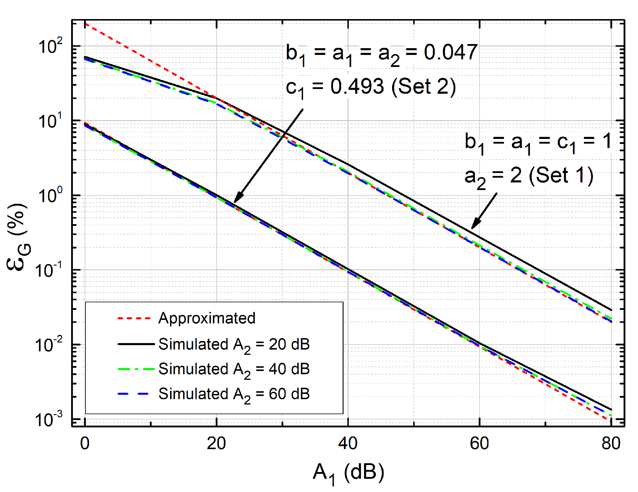
In the final approximation given in Equation (2), we made the assumption that , which is reasonable even for inverter-based circuits. It is important to highlight that, by this approximation, G is a function of only and of coefficients and . Figure 2 shows the gain error curves for different values of , , confirming the very slight dependence of G on . Moreover, two families of curves can be distinguished for the two different sets of coefficients indicated in the figure.
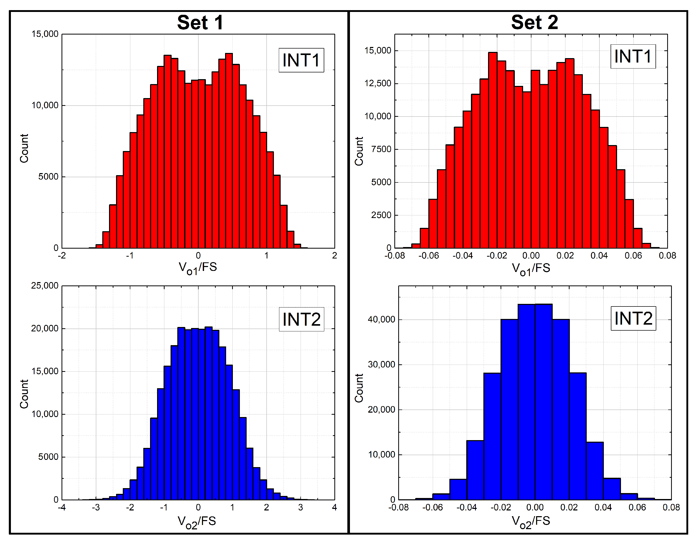
The choice of these values is here briefly discussed. A first set (, ) can be easily calculated from the linearized z-domain model of Figure 1 starting from the approximation of infinite DC gain (i.e., ), in order to obtain a flat and a Noise Transfer Function () with two zeros at the origin. However, with this set of coefficients (from now on indicated as “Set 1”), the modulator state variables and are not bounded to remain within the full-scale range of the ADC, as shown in Figure 3. Since the full-scale range is typically equal or on the order of the supply voltage, this would imply large harmonic distortions due to the limited linear output ranges of the amplifiers employed in the integrators.
To overcome this issue, the modulator coefficients can be properly scaled in order to limit the state variables [39]. An example of scaled coefficients, here called “Set 2”, is represented by , . It is worth mentioning that, working with low supply voltages and consequently low voltage headrooms, the attenuation introduced by the modulator coefficients becomes increasingly essential. The linear output range of an amplifier can be roughly considered to end at voltages where one of the output devices exits saturation region. Considering, for instance, a simple voltage amplifier as the CMOS inverter, the linear output range is limited by a saturation voltage from both rails. , which in strong inversion corresponds to the overdrive voltage , can be assumed around in weak inversion [40], where is the equivalent thermal voltage, k is the Boltzmann constant, T is the absolute temperature, and q is the electron charge. mV at room temperature, then mV in weak inversion. Outside the linear output range, the output resistance rapidly decreases and consequently also the DC gain, increasing also the distortion introduced by the amplifier. For supply voltages approaching , the linear output range becomes increasingly narrow, thus forcing a more aggressive scaling of the modulator coefficients. The Set 2 introduced before, for example, has been obtained in order to have a state variable swing equal to 15% of the full-scale range, as confirmed by the histograms in Figure 3.
Actually, the coefficient sizing impacts not only on the converter linearity, but even on other parameters, for example on the gain error as shown in Figure 2. A lower ratio as in the case of the scaled coefficients used here, involves a lower gain error, as described also by Equation (2). Nevertheless, in order to achieve a negligible gain error for an ADC with moderate resolution, thus avoiding expensive calibration procedures, a DC gain of the first integrator higher than 40–50 dB is still needed in even employing the second set of coefficients.
2.2. Dead-Zones
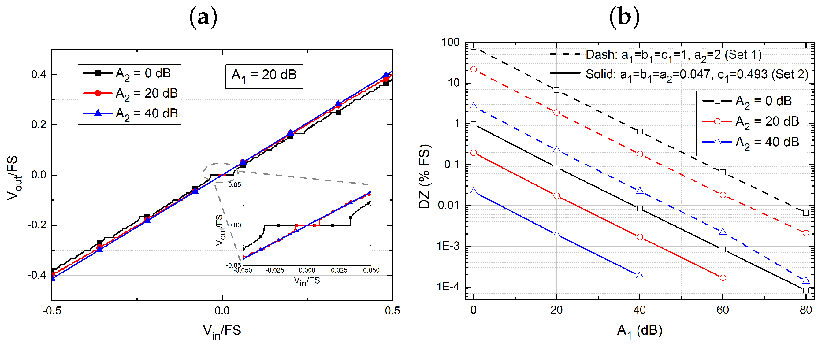
As is known, the integrator DC gain also affects the width of Dead-Zones (DZs). Differently from the gain error, DZs depend significantly on the DC gain of both integrators in a 2nd order modulator [39]. It is worth noting that, even in this case, the modulator coefficients have an influence on the DZs. Figure 4a shows the DC characteristics of the modulator with the first set of coefficients, for dB and different values of . For the curve with the lowest value of , dead-zones are visible for several DC inputs. In the inset, the scaling of the dead-zone amplitude for increasing value of is visible. Figure 4b shows the amplitude of the dead-zone located around the middle of the converter input range, which is the widest of all the other dead-zones present in the ADC characteristics. Two families of curves are plotted for the two sets of coefficients previously discussed. With Set 2, for the same values of and , the DZ is much smaller than in the case of Set 1. In both cases, however, the DZ is approximately inversely proportional to the product of and . For this reason, if large DC gains are employed for gain error issues, relative low gains are allowed without running into significant distortion due to DZs, especially employing the scaled coefficients.
2.3. Quantization Noise
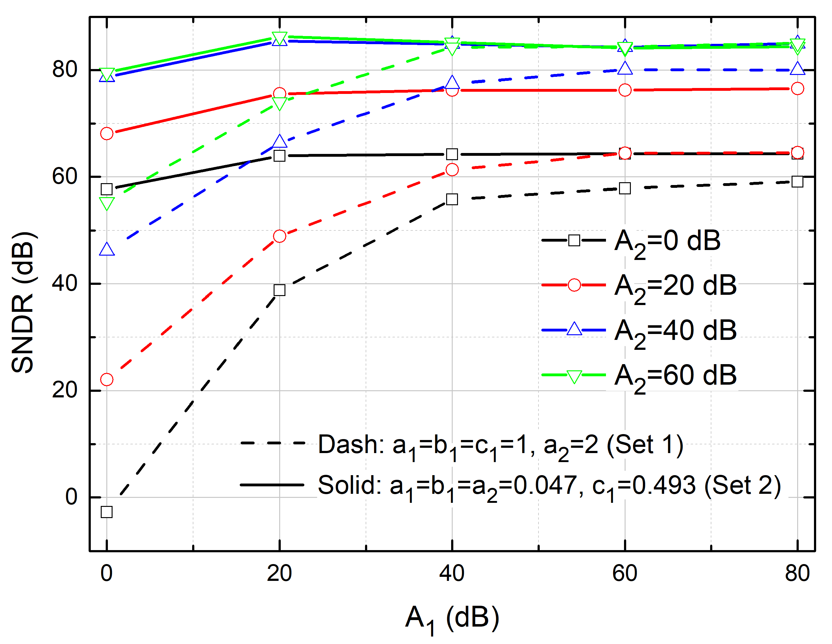
A phase error in the integrators due to their limited DC gain causes the shifting of the two zeros in the , thus increasing the overall quantization noise power. Figure 5 shows the SNDR of a 2nd order modulator, with a −2 dBFS input tone and an OverSampling Ratio (OSR) of 128 for the two different sets of coefficients already discussed.
Considering the curves obtained employing Set 1, the maximum values of SNDR are reached for values of DC gains and higher than 60 dB. Conversely, the scaled coefficients of Set 2 allows for achieving the same values, but with a lower DC gain of both integrators. It is worth mentioning that for the lowest values of and , especially with Set 1, dead-zones contribute to worsen the SNDR.
Even if the scaled coefficients guarantee better performances in terms of DC gain, dead-zones, and quantization noise suppression, mitigating the effect of finite DC gain of the amplifiers, it is not advisable to rely only on the values of the coefficients. Since the modulator coefficients are typically implemented as capacitive ratios in the SC integrators, too small values may be particularly detrimental for the modulator performances. When the converter resolution is limited by thermal noise, the absolute value of the input capacitors, responsible for the signal sampling, is sized according to noise specification. This is particularly critical in ULV scenarios, where the signal range is limited by the decreasing supply voltage and then, targetting the same resolution, the requirements on the converter noise becomes stricter. Consequently, small modulator coefficients enlarge the values of the feedback capacitors of the SC integrators, thus impacting on area and power consumption.
2.4. Low-Frequency Noise and Offset
Error sources and of Figure 1 affect the converter performances through two different , which can be evaluated analogously to the traditional for the quantization noise , considering the linearized block diagram of Figure 1 [41]. While offset and noise of the first integrator are not attenuated by the modulator response, the contributions of the second integrator are intrinsically high-pass filtered, thus giving negligible contributions in the signal bandwidth. For this reason, dynamic offset cancellation techniques, such as CHopper Stabilization (CHS) and correlated double sampling, are typically applied only to the first integrator. CHS represents a popular approach in modulators [12], thanks to the possibility of exploiting the digital low-pass decimator filter cascaded to the modulator, which also rejects to the offset ripple by proper choice of the chopping frequency and OSR. However, CHS modulation introduces several drawbacks, among which the worse settling time due to the parasitic capacitances of the demodulator switches. A typical solution is to place the chopper demodulator at non-dominant poles, as at the sources of the common-gate stage in the cascode structure [42]. In single-stage ULV and ULP amplifiers, where demodulation can be realized only at the output nodes, characterized by very high output resistance, CHS may have detrimental effects on the resulting DC gain of the amplifier. The SC integrator presented in [28] combines a CDS mechanism with a novel topology aimed at reducing the transfer function sensitivity to the amplifier DC gain, thus alleviating the above-mentioned issues related to modulators.
3. Modulator Architecture
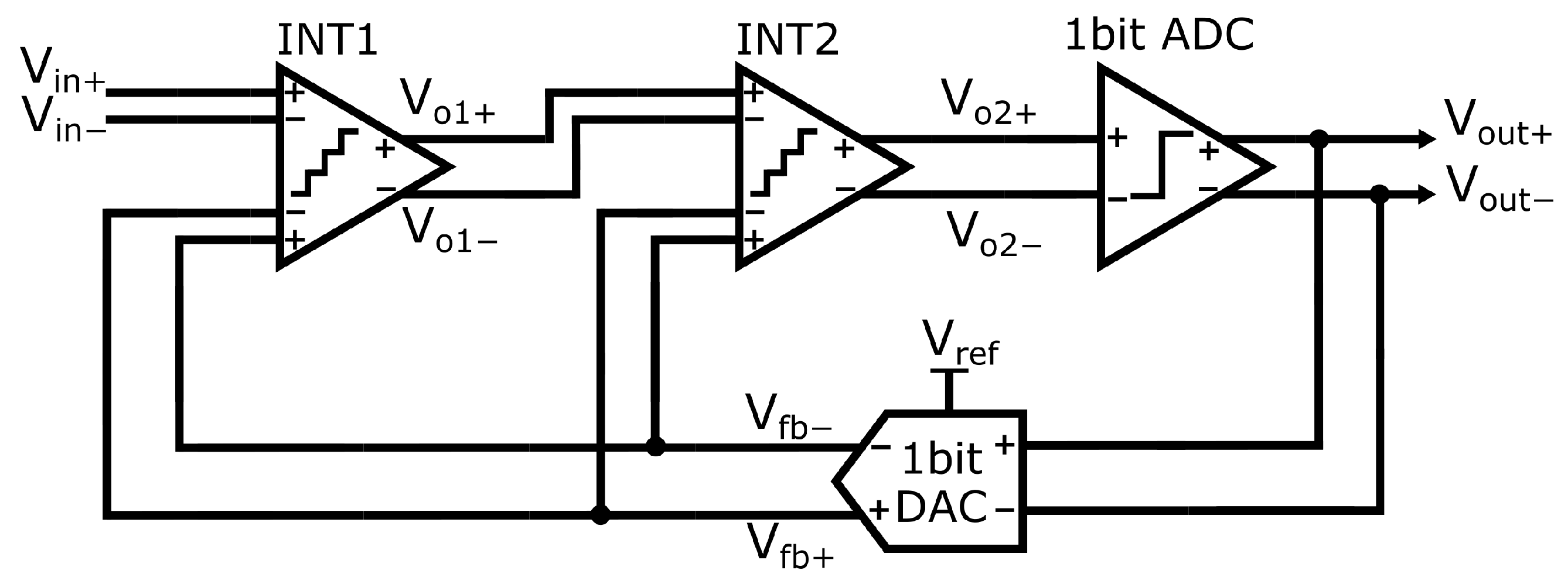
A block diagram of the modulator is depicted in Figure 6. It is a 2nd order, single-bit, inverter-based, fully-differential topology: There are two integrators (INT1 and INT2), a 1-bit ADC and a 1-bit Digital-to-Analog Converter (DAC). A second order architecture was chosen because it represents a good compromise among resolution increase and simplicity; in addition, it is intrinsically stable.
The modulator was designed for an ultra-low supply voltage V. We will now analyze every single block in more detail.
3.1. Integrators
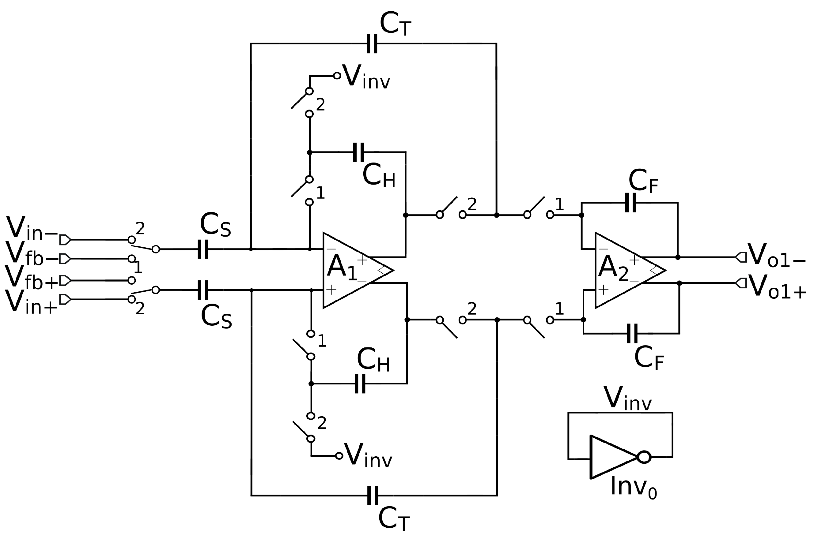
For the first integrator INT1, we adopted the topology of Figure 7 [28]. This architecture was already used in single-ended ULV modulators [9,29], but not yet in a FD implementation.
Every switch is closed during the phase corresponding to the number near to it, while A1 and A2 are inverter-based FD amplifiers that will be described later.
Due to the symmetry of the circuit, it is possible to restrict the analysis to the lower half. The input capacitor CS samples and , at the end of clock phases 2 and 1, respectively. A charge proportional to flows into CT during phase 2. In the following, phase 1, the charge stored in CT is transferred to CF in the second stage, which behaves as an accumulator. This produces an increment of the output voltage , so that an integration step is completed. Thanks to the CH contribution, which holds the voltage at the output of the first amplifier during phase 1 avoiding its reset, the charge transfer is a little sensitive to the DC gain of the first amplifier, as proposed in [43]. Considering also the second stage, the integrator produces an overall DC gain proportional to the cube of the gain of the single amplifier [28]. This aspect makes this SC topology particularly interesting for ULV modulators, thus relaxing the requirements on the DC gain of the employed amplifiers. Even single-stage inverter-like topologies with short channel lengths, with DC gain on the order of tens or lower, can be usefully exploited. Another advantage of the proposed integrator is the mentioned CDS technique, capable of rejecting the offset and reducing the flicker noise of both the amplifiers, improving low frequency accuracy and resolution.
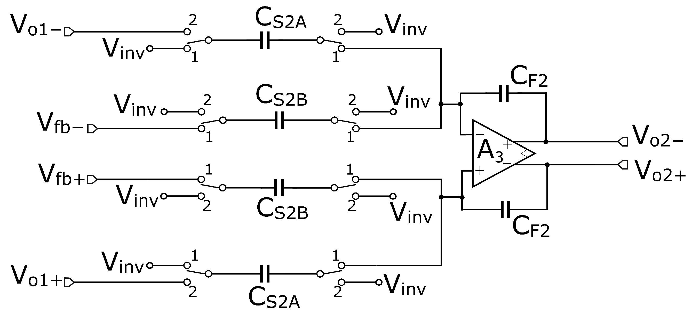
As widely explained in the previous section, converter gain error depends almost exclusively on the first integrator. Moreover, since the dead-zone amplitudes and the zeros’ shift in the NTF depend on the product of both and , the high-gain SC integrator has been employed only for the first integrator. Even noise and offset requirements for the second integrator are more relaxed, thus no dynamic offset cancellation techniques are needed. For all these reasons, it was possible to adopt a simpler topology for the second integrator, such as the parasitic-insensitive one [38] as depicted in Figure 8 in its FD version. Due to the different coefficients and implemented in the SC integrator, the number of input sampling capacitors is doubled.
Finally, a simple diode-connected inverter (Inv0) generates the constant bias voltage Vinv depicted in Figure 7. This voltage is connected to CH during phase 2, in order to minimize the voltage excursion of CH bottom terminal in the transition between the two clock phases; it is also employed in the second integrator INT2 as a reference common-mode voltage.
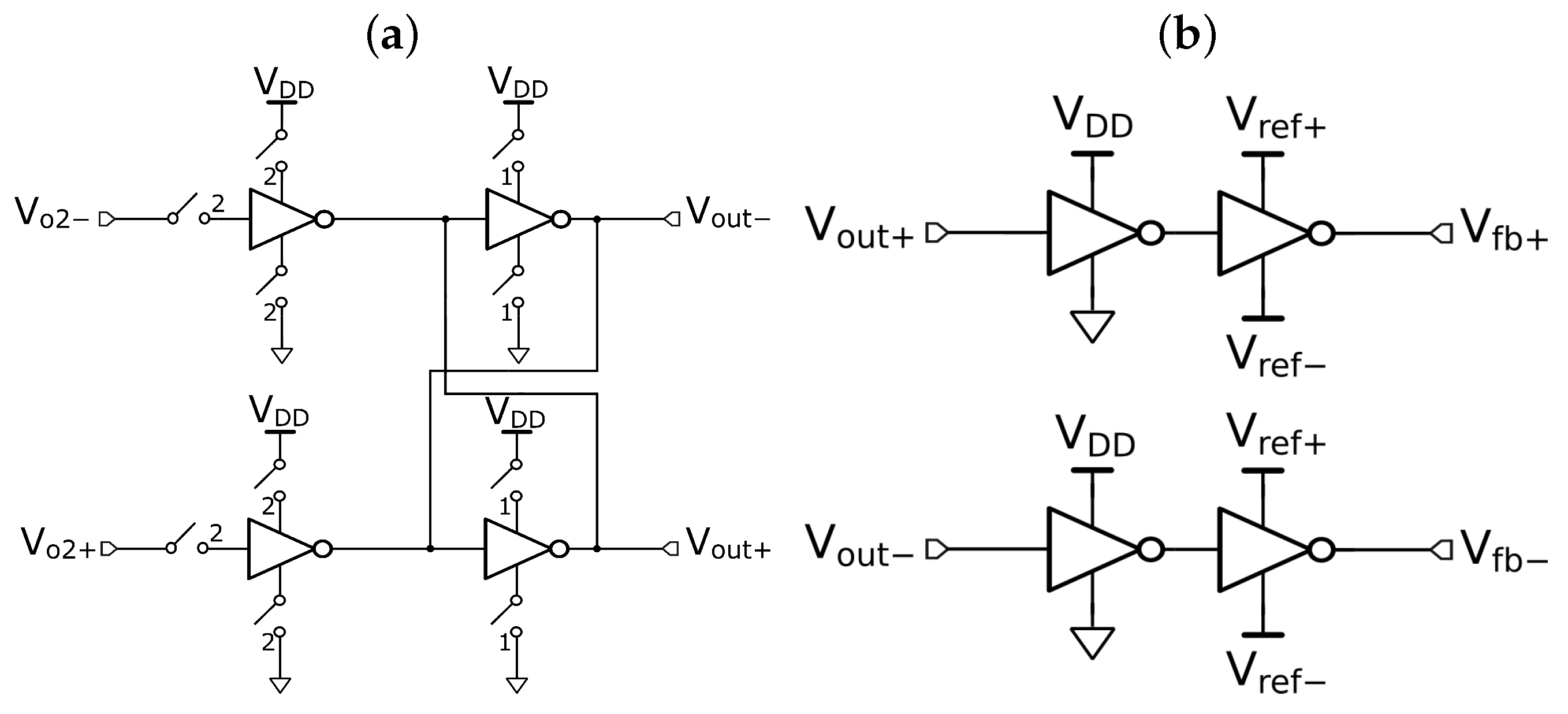
3.2. ADC and DAC
The ADC and the DAC are 1-bit architectures, visible in Figure 9a,b, respectively. The 1-bit ADC internal to the modulator is simply a comparator. The input signal is pre-amplified by the input inverters, then the two inverters in a latch fashion exploit the positive feedback to take the decisions and regenerate the full-logical values for the output bitstream. The 1-bit DAC is simply the cascade of two inverters, where the first one acts as an inverting buffer and the second one provides the differential feedback voltages and . and represent the differential reference voltages of the modulator. In this work, we opted for a ratiometric converter; in this way, and correspond to the supply voltage and ground, respectively.
3.3. Clock-Boosting Circuit
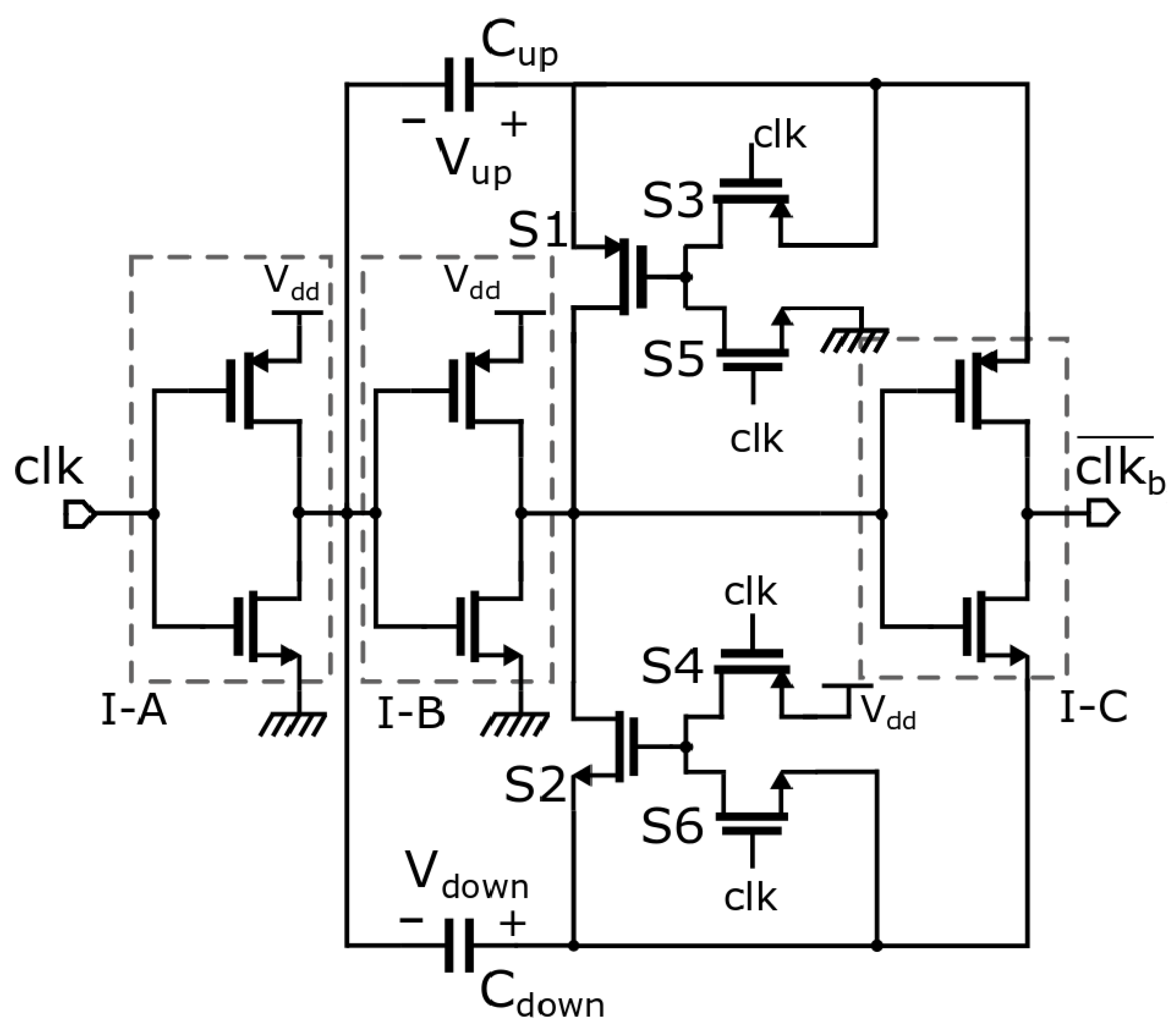
The switches of the circuit were mostly implemented as complementary pass-gates. The ULV domain is detrimental for the on-resistance of the MOSFETs in the triode region. Increasing the aspect ratio to reduce the pass-gate on-resistances impacts the linearity performances of the circuit due to larger parasitic capacitances and charge injection issues. This design takes advantage from a clock-boosting technique capable of level-shifting both the high and the low levels of the clock signals driving the pass-gates. The circuit is visible in Figure 10 and a more detailed analysis is provided in [9].
3.4. Inverter-Based Amplifier
As already stated, the CMOS inverter may be used as a replacement of a voltage amplifier, as demonstrated in [9]. A FD version of the inverter-like amplifier requires that its output CM is stabilized, in order to prevent possible drifts and, consequently, a degradation of the output Differential-Mode (DM) range. A well-known solution is represented by the Nauta transconductor [44], but many others are available in the literature [45]. In this work, we adopted the amplifier recently proposed in [27], which has an increased output linear range with respect to other solutions. Its schematic view is shown in Figure 11. It was employed in both INT1 and INT2 for A1, A2, and A3.
Inv1 and Inv2 are the inverters that process the input differential signal and are nominally identical. The other inverters Inv3-9 are part of the stabilization loop. Again, for symmetry purposes, Inv3 needs to match Inv4, and the same applies for Inv5 and Inv6.
The CMSL was thoroughly analyzed in [27]; here, we will briefly summarize its principle of operation. Assuming ideal matching between the inverters, the loop does not affect the output DM, apart from an attenuation of the output resistance due to the presence of and . Inv3 and Inv4 produce a voltage that, as far as small signals are concerned, depends only on the output CM. Then, Inv7 and Inv5/6 close the loop. Even in the case of large output differential modes that are going to affect node , the feedback loop has a very small impact on the differential mode gain, since Inv5/6 produce only common-mode effects. Inv8 and Inv9, instead, act as load for Inv3/4 and Inv7, respectively, in order to reduce the loop gain and avoid instability. This is needed because there are two loops formed by the cascade of three inverters, that are Inv3-7-5 and Inv4-7-6.
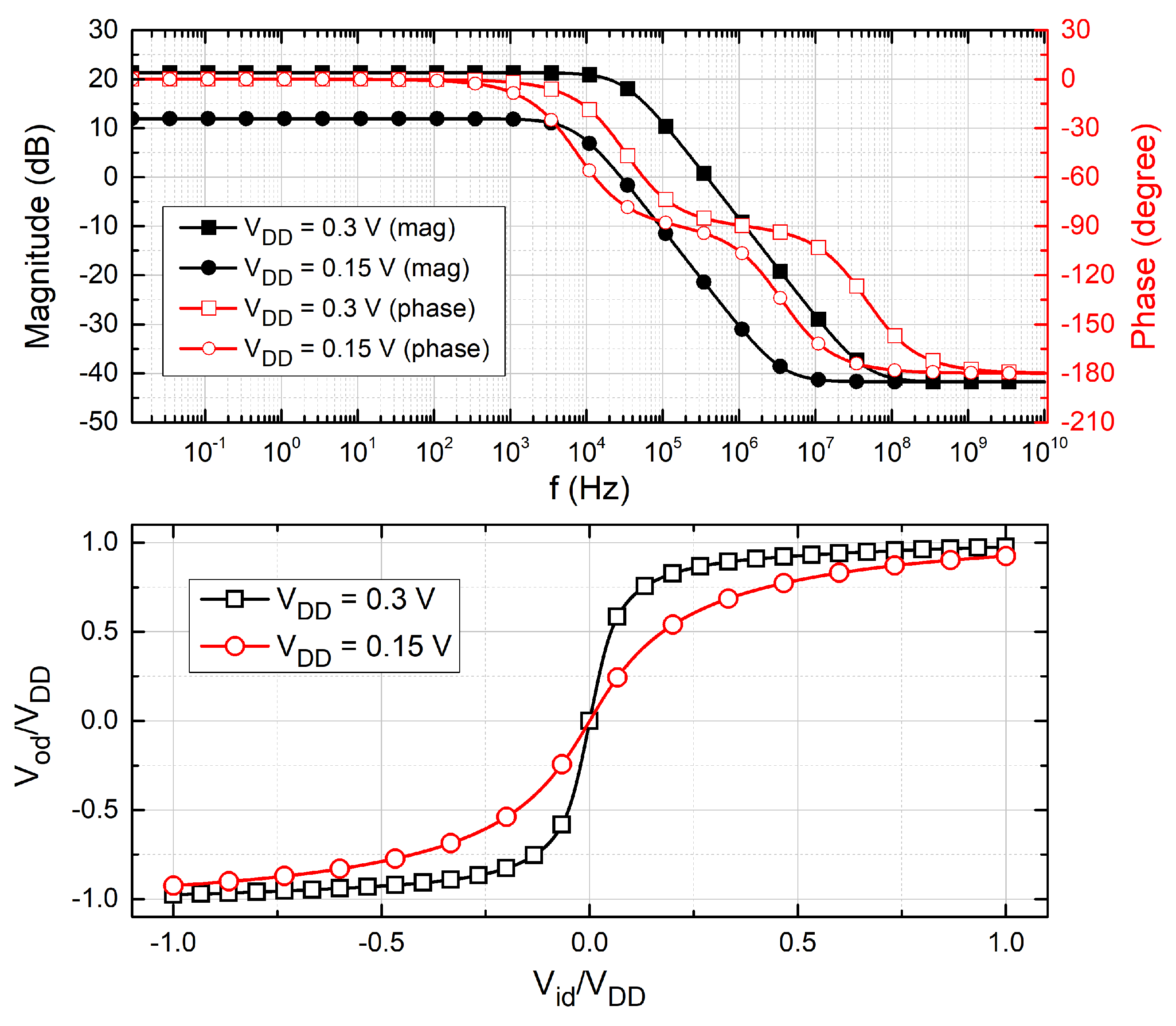
Figure 12 shows the simulated Bode diagrams and the dc characteristics, with a supply voltage of 0.3 V and 0.15 V. The amplifier DC gain, already lower than 20 dB at V, is around only 12 dB at V. The Gain-BandWidth product (GBW) is also reduced by nearly a factor of 10, due to the exponential dependence of the quiescent current on . The input-output differential characteristics at the two different supply voltages depicted in Figure 12 show that, besides the different gain around V, the linearity range of the amplifier is also obviously smaller at the lowest supply voltage.
3.5. Device Sizing
The modulator was designed with the 0.18-μm UMC CMOS process, with the device parameters shown in Table 1. Minimum channel lengths were adopted in order to improve speed performances. Body biasing for pMOS transistors of the inverter-like amplifiers was employed to enhance the maximum operating frequency; in particular, their bodies were connected to ground in order to reduce their threshold voltages and consequently moderate the request for high aspect ratios, typically larger than the nMOS to counteract the lower mobility. The same technique is not suitable for the nMOS devices, due to the absence of a p-well isolated from the substrate in the used technology. Thanks to the clock-boosting circuit, it was possible to assign a reasonably low width to the pass-gates, thus keeping under control charge injection issues, as well as the parasitic capacitances. As for the amplifier inverters Inv1 and Inv2 of Figure 11, instead, high aspect ratios are needed to reach a sufficient GBW. The other inverters Inv3-9 were sized with the same strategy described in [27]. The diode-connected inverter Inv0, which provides the constant bias voltage Vinv (close to ), is a scaled version of Inv1,2.
The capacitors represent the main contribution to the estimated total area occupation of the modulator. We tried to keep them as small as possible, but with some limitations. The value of the sampling capacitors CS of the first integrator impact directly on the converter thermal noise. Another constraint is represented by the ratios CS/CF, CS2B/CF2, and CS2A/CF2, sized equal to , , and , respectively. The coefficient set used in this design corresponds to the Set 2 discussed in Section 2. Their values are summarized in Table 2, resulting in an estimated area of 0.03 mm2, obtained by summing up the area occupied by all components, excluding the interconnections. Note that, in the technology used in this work, active devices can be placed below the Metal-Insulator-Metal (MIM) capacitors, which turn out to be the dominant factor. For this reason, the area estimation of the proposed ADC coincides with the capacitor area. Cup and Cdown were not included in this area estimation, because they are not properly part of the modulator: The clock boosting circuit, in fact, may be shared among several blocks in a complete ULV data acquisition system. They are equal and were set to 1 pF.
4. Simulation Results and Discussion
The modulator was validated by means of electrical pre-layout simulations performed with Cadence SpectreTM; in particular, transient noise simulations have been performed in order to also take into account electrical noise. In all simulations, the supply voltage and OSR were set to 0.3 V and 128, respectively, if not otherwise specified. The bitstream was processed by a VerilogA decimation filter to extract the output codes. We will call PI a modulator where, for the first integrator, a standard parasitic-insensitive architecture [38] is employed, with the amplifier, the sampling capacitor, and the capacitive ratios kept unchanged. The performances of the PI modulator will be compared with our proposed modulator, in order to highlight the benefits of the high-gain SC integrator depicted in Figure 7.
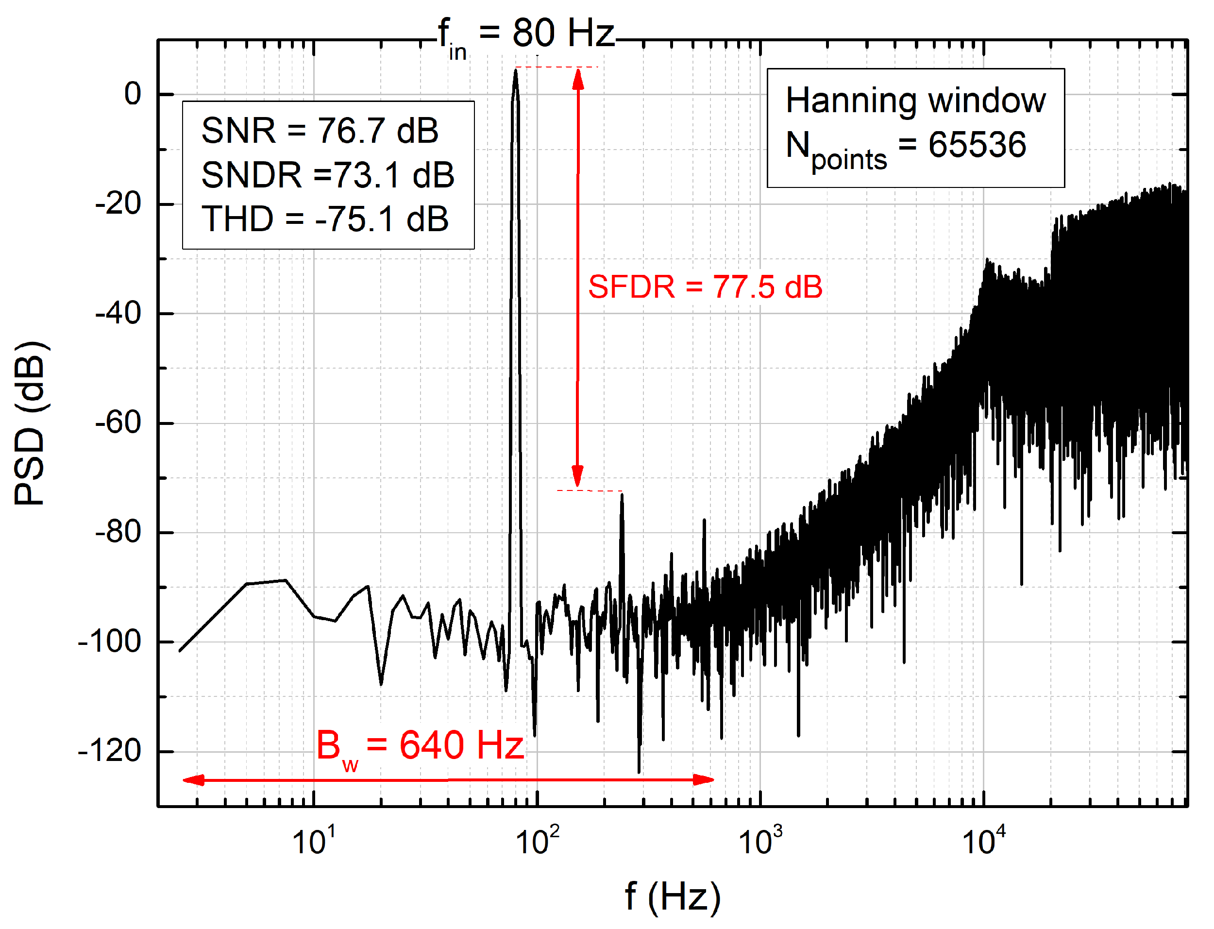
The spectrum of the output bitstream is plotted in Figure 13, where the input is a sinusoidal waveform with frequency 80 Hz and peak-to-peak (p-p) amplitude 450 mV. The clock frequency is set to 164 kHz. The SNR and SNDR resulted to be 76.7 dB and 73.1 dB, respectively. The Total Harmonic Distortion (THD), defined as the ratio between the distortion and the input signal power PTHD/PIN, was about −75 dB. Excluding the clock-boosting circuit, the power consumption PD was equal to only 200.5 nW. The Schreier Figure of Merit (FoM) can be calculated as:
which is among the best ones of ULV modulators.
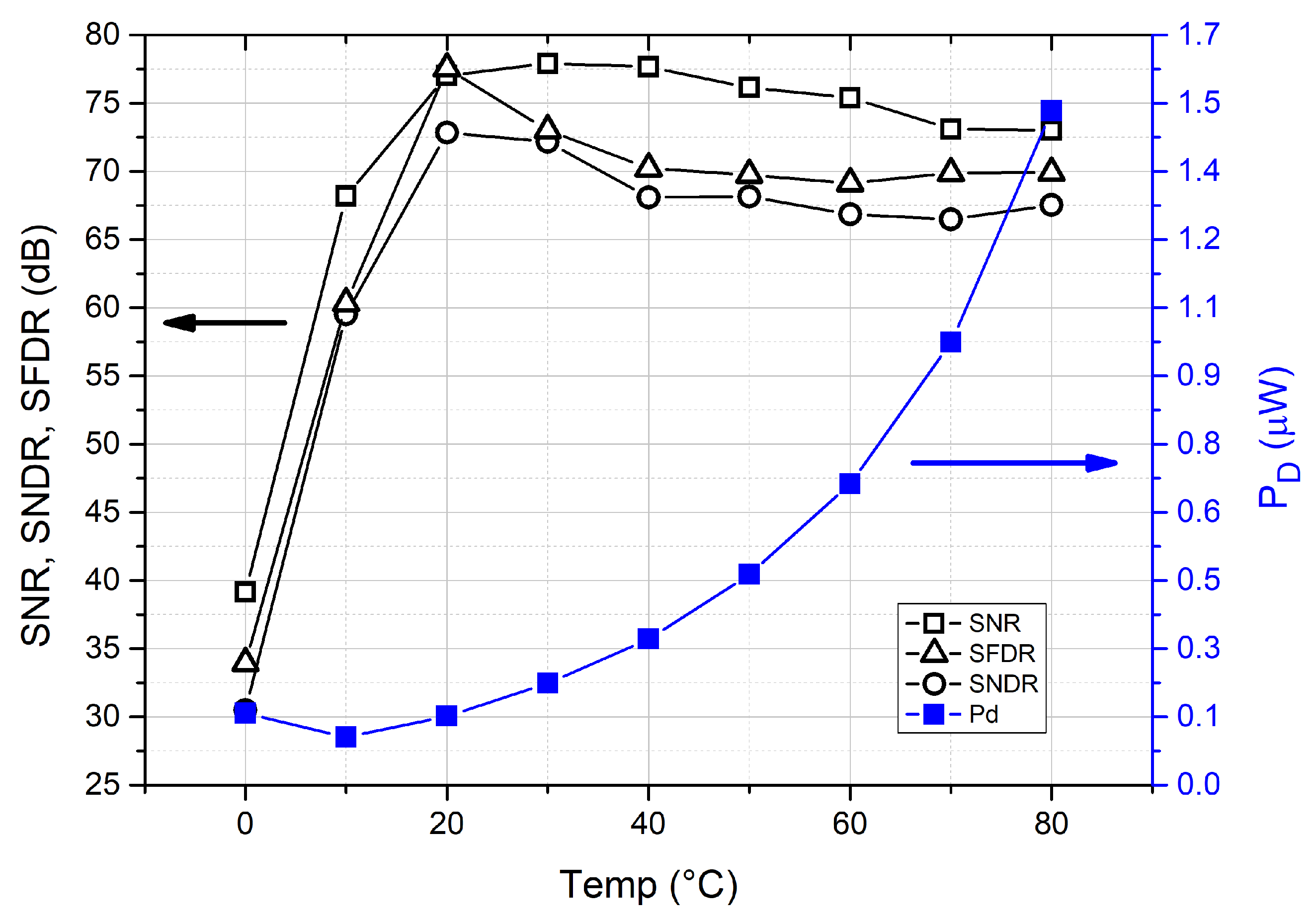
The DC transfer function was also extracted, in order to assess the gain error G: The results are visible in Figure 14. In the proposed architecture, G resulted to be 60 times lower than in the PI modulator, being equal to just 0.014%. The gain error improvement is consistent with the low DC gain sensitivity of the employed SC integrator, that is inversely proportional to the cube of the inverter-like amplifier DC gain. Furthermore, a temperature sweep was conducted and Figure 15 shows the results of this simulation. The dissipated power has an exponential dependence with the temperature, as expected by the weak inversion bias region of the inverter-based amplifiers. For the same reason, the amplifier bandwidth has a similar exponential behavior with temperature, explaining the worsening of the modulator dynamic performances at the lowest temperatures.
The Power Supply Rejection Ratio (PSRR) has been tested by superimposing a sinusoidal waveform with a 10-mV amplitude at different frequencies on the nominal supply voltage, not affecting the reference voltages and . Each point of the PSRR curve plotted in Figure 16 is evaluated by averaging over the PSRR values obtained from 200 Monte Carlo (MC) runs. Nominal simulations, in fact, are useless to estimate the actual PSRR of the circuit, due to the symmetry of the FD modulator. The error bars represent the minimum and the maximum PSRR values obtained from the 200 MC runs, for each ripple frequency. Moreover, considering the ratiometric operation of the ADC, we performed an additional test by feeding the input with a constant fraction () of the supply voltage. In the ideal case, this should result in a constant output code ( of full scale). The actual variation estimated by varying across the interval 0.27–0.33 V was lower than of full scale, proving that low sensitivity to supplies voltage variations.
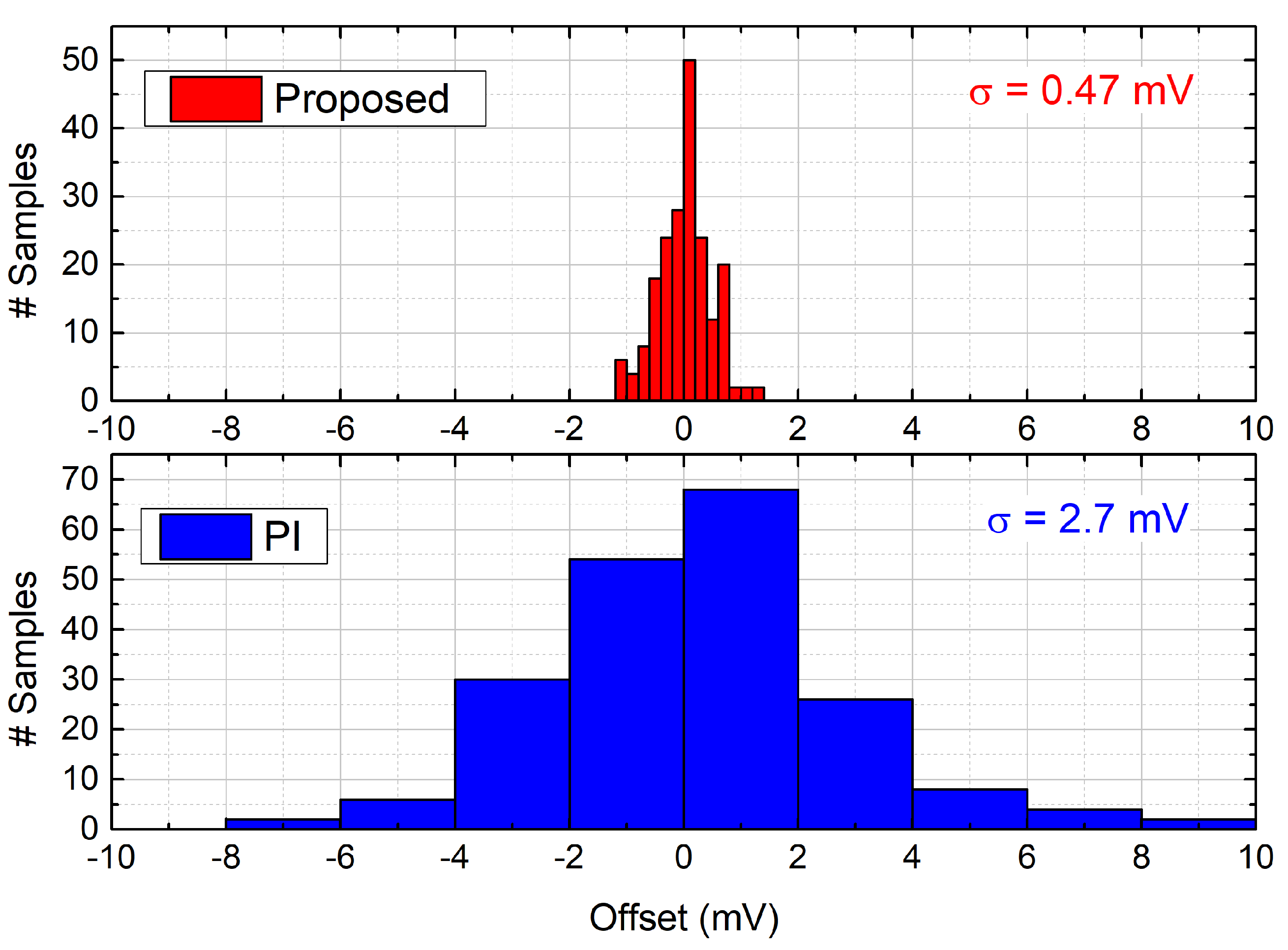
MC simulations were also performed to evaluate the offset of the modulator. The offset mean value estimated over 200 MC runs is 16 μV, and the standard deviation is 0.47 mV. A histogram that describes this spread is depicted in Figure 17, where it is also shown how the offset changes for the PI modulator. In the latter case, the standard deviation increases by a factor greater than 5.7, demonstrating the effectiveness of the CDS technique intrinsically operated by the first integrator.
Table 3 summarizes the spread of the most relevant parameters over corner variations. Due to the sub-threshold operation of the devices, the amplifier bias current exhibits very large relative variations against process spread (mainly due to threshold voltage variations), strongly affecting the maximum operating frequency. For this reason, the frequencies at which the parameters in Table 3 have been determined are different for each corner. It is worth noting that, in the SS corner, the modulator dissipates less power but is capable of working with a sampling frequency around four times lower than in the typical corner. Analogous considerations explain the performances in the FF corner, while the condition of Slow NMOS/Fast PMOS represents the worst case in terms of distortion.
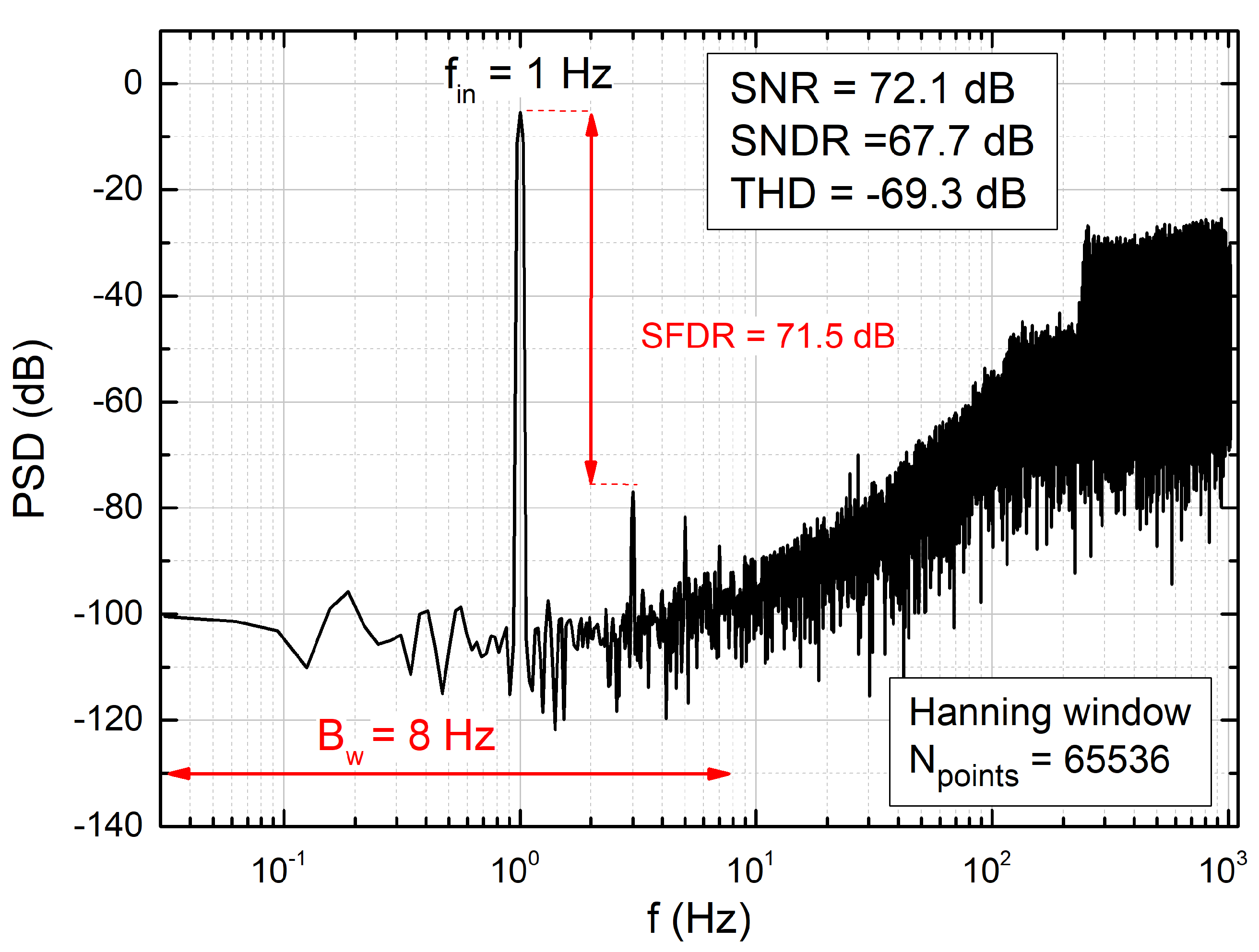
The modulator was designed with the target supply voltage of 0.3 V, but it is interesting to check its performances with a much lower supply voltage. Figure 18 shows the output bitstream spectrum at = 0.15 V, when the input is a sinusoidal waveform with frequency 1 Hz and p-p amplitude 112.5 mV. The clock frequency is set to 2 kHz.
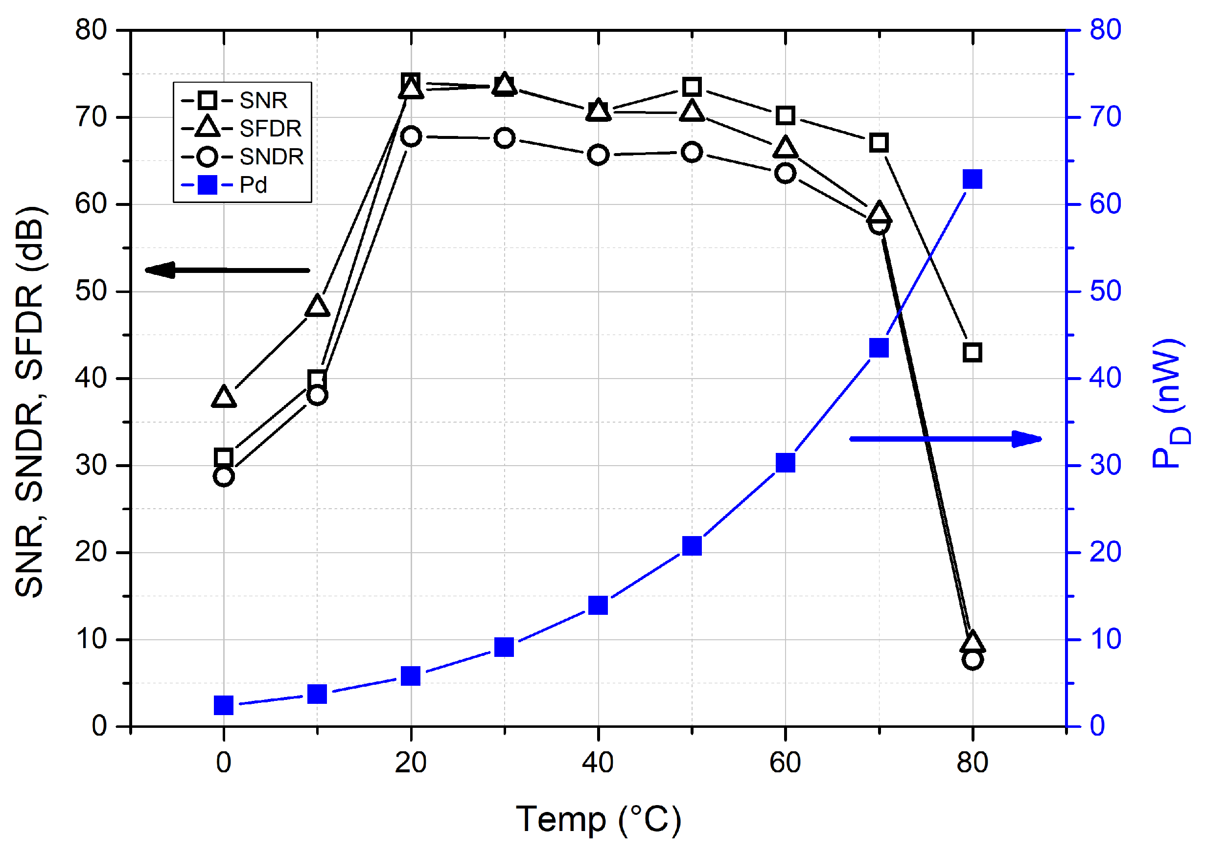
In these operating conditions, the modulator managed to achieve an SNR of 72.1 dB and an SNDR of 67.7 dB, with a power consumption of just 8.06 nW. The latter was reduced by nearly a factor of 25, but also the maximum clock frequency decreased (and thus the bandwidth). The resulting FoM was 158 dB, which is still a good value among ULV modulators. A temperature sweep was conducted also with = 0.15 V and the results are shown in Figure 19. The modulator behaviour is similar to the one shown in Figure 15 up to 60 C, where the dynamic performances start to drop due to the increase of the leakage currents, which disrupts correct operations of clock boosters. Concerning the effects of supply voltage variations, we fed the ADC input with a voltage equal to and varied VDD from 0.14 V to 0.16 V. The maximum variation of the output code across this range was about of full scale, revealing that reducing to this extremely low value increases the sensitivity to supply voltage.
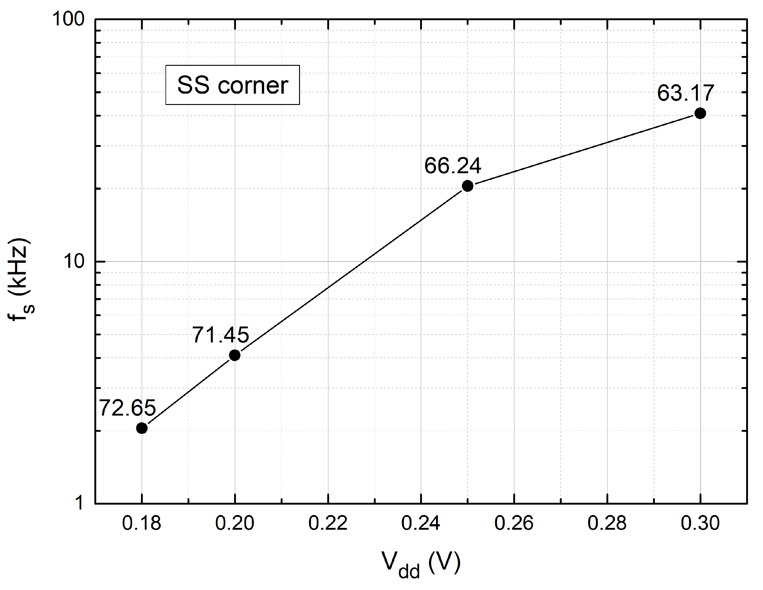
Investigating the effects of process variations showed that, at = 0.15 V, it was impossible to find a sampling frequency where the ADC works properly, when SS, SNFP, and FNSP corners were considered. For these corners, correct operations of the modulator would require a further clock frequency reduction. Unfortunately, due to the leakage currents, the clock boosters are not capable of maintaining correct clock levels for such low frequencies. We focused on the worst case corner, the SS one, finding out that the lowest acceptable value of was 0.18 V. In Figure 20, we show the sampling frequency for the four supply voltage points. For each supply voltage/sampling frequency combination, we indicated also the SNDR. We could not find a convincing reason for the increase of SNDR at lower supply voltages (and slower sampling frequencies).
In a similar way to the case of higher supply voltage, we performed MC simulations to evaluate the offset of the modulator at = 0.15 V. The offset mean value estimated over 200 MC runs is −27.5 μV, and the standard deviation is 0.82 mV. Figure 21 shows the histogram of offset spread compared to the PI modulator, under the same supply voltage condition. As seen for = 0.3 V, the proposed modulator shows better performances compared to the solution employing the traditional integrator topology.
In order to predict the possible advances that can be obtained by means of the proposed architecture in the field of ULV data converters, the simulation results obtained in this work have been compared in Table 4 with other state-of-the-art ULV ADCs. Table 4 includes previous works on modulators based on different approaches, namely DT, Continuous-Time (CT), Voltage-Controlled Oscillator (VCO)-based, and Current-Controlled Oscillator (ICO)-based.
From the comparison, it appears that the proposed architecture can produce values of the FoM very close to the best literature result [26], while being able to work with a considerably lower supply voltage. The total power consumption is also very close to the best figure [5] in Table 4, which makes the proposed modulator a promising solution for a large variety of energy harvesting applications and, in particular, for ultra-low voltage sources, as biofuel cells. It is worth highlighting that, while other works of Table 4 present measurement outcomes, our results are projections based on electrical simulations, aimed at assessing the modulator functionality and its robustness with respect to PVT variations.
5. Conclusions
Important modulator issues such as gain error, dead-zones, degradation of noise-shaping function, low-frequency noise, and offset introduce severe penalties on the overall performances of ADCs. By means of high-level simulations, we discussed the impact of these non-idealities especially when related to ultra-low voltage scenarios, focusing on the effect of the integrator finite DC gain and the modulator coefficients. In order to counteract some of the above mentioned issues, we designed a modulator capable of working with ultra-low supply voltages, which takes advantage of a high-DC gain switched-capacitor integrator and a fully-differential inverter-like amplifier, both recently proposed. In the nominal corner, it reached an SNDR of 73 dB, with a clock frequency of 164 kHz and a dissipated power of only 200.5 nW, at a supply voltage of 0.3 V: The Schreier’s FoM reached 168.1 dB. Its gain error was also estimated and resulted in just 0.014%, while the offset had a standard deviation of 470 μV. The benefits introduced by the employed switched-capacitor integrator topology with respect to a standard one were highlighted. Simulations over different process corners, temperatures, and supply voltage variations were used to estimate the spread of the main performance parameters, in particular showing some critical issues when coming to lower supply voltages, down to 0.15 V. The performances of this modulator make it extremely useful in the energy harvesting scenario, as, for example, in a biofuel cell-powered system.
Author Contributions
All authors participated to the conceptualization and methodology of this work. Data curation, L.B., A.R.; writing—original draft preparation, L.B., A.C., G.M.; writing—review and editing: M.P., P.B. All authors have read and agreed to the published version of the manuscript.
Funding
This research received no external funding.
Conflicts of Interest
The authors declare no conflict of interest.
References
- Alioto, M. Enabling the Internet of Things: From Integrated Circuits to Integrated Systems; Springer International Publishing: Berlin/Heidelberg, Germany, 2017. [Google Scholar]
- Dao, V.-D. An experimental exploration of generating electricity from nature-inspired hierarchical evaporator: The role of electrode materials. Sci. Total Environ. 2021, 759, 143490. [Google Scholar] [CrossRef]
- Dao, V.D.; Vu, N.H.; Dang, H.L.; Yun, S. Recent advances and challenges for water evaporation-induced electricity toward applications. Nano Energy 2021, 85, 105979. [Google Scholar] [CrossRef]
- Odkar, A.J.; You, J.M.; Kim, N.H.; Gu, Y.; Kumar, R.; Mohan, A.V.; Kurniawan, J.; Imani, S.; Nakagawa, T.; Parish, B.; et al. Soft, stretchable, high power density electronic skin-based biofuel cells for scavenging energy from human sweat. Energy Environ. Sci. 2017, 10, 1581–1589. [Google Scholar]
- Yeknami, A.F.; Wang, X.; Jeerapan, I.; Imani, S.; Nikoofard, A.; Wang, J.; Mercier, P.P. A 0.3-V CMOS Biofuel-Cell-Powered Wireless Glucose/Lactate Biosensing System. IEEE J. Solid Circuits 2018, 53, 3126–3139. [Google Scholar] [CrossRef]
- Shih, Y.C.; Otis, B.P. An Inductorless DC–DC Converter for Energy Harvesting With a 1.2-μW Bandgap-Referenced Output Controller. IEEE Trans. Circuits Syst. II Express Briefs 2011, 58, 832–836. [Google Scholar] [CrossRef]
- Yeknami, A.F. A 300-mV ΔΣ Modulator Using a Gain-Enhanced, Inverter-Based Amplifier for Medical Implant Devices. J. Low Power Electron. Appl. 2016, 6, 4. [Google Scholar] [CrossRef] [Green Version]
- Michel, F.; Steyaert, M.S.J. A 250 mV 7.5 W 61 dB SNDR SC ΔΣ Modulator Using Near-Threshold-Voltage-Biased Inverter Amplifiers in 130 nm CMOS. IEEE J. Solid Circuits 2012, 47, 709–721. [Google Scholar] [CrossRef]
- Catania, A.; Benvenuti, L.; Ria, A.; Manfredini, G.; Piotto, M.; Bruschi, P. A 2 nW 0.25 V 140 dB-FOM Inverter-Based First Order ΔΣ Modulator. IEEE Trans. Circuits Syst. II Express Briefs 2020, 67, 1514–1518. [Google Scholar] [CrossRef]
- Kulej, T.; Khateb, F.; Kumngern, M. 0.3-V Nanopower Biopotential Low-Pass Filter. IEEE Access 2020, 8, 119586–119593. [Google Scholar] [CrossRef]
- Nishi, M.; Matsumoto, K.; Kuroki, N.; Numa, M.; Sebe, H.; Matsuzuka, R.; Maida, O.; Kanemoto, D.; Hirose, T. A 34-mV Startup Ring Oscillator Using Stacked Body Bias Inverters for Extremely Low-Voltage Thermoelectric Energy Harvesting. In Proceedings of the 2020 18th IEEE International New Circuits and Systems Conference (NEWCAS), Montréal, QC, Canada, 16–19 June 2020; pp. 38–41. [Google Scholar] [CrossRef]
- Tan, Z.; Chen, C.H.; Chae, Y.; Temes, G.C. Incremental Delta-Sigma ADCs: A Tutorial Review. IEEE Trans. Circuits Syst. I Regul. Pap. 2020, 67, 4161–4173. [Google Scholar] [CrossRef]
- Rodovalho, L.H.; Aiello, O.; Rodrigues, C.R. Ultra-Low-Voltage Inverter-Based Operational Transconductance Amplifiers with Voltage Gain Enhancement by Improved Composite Transistors. Electronics 2020, 9, 1410. [Google Scholar] [CrossRef]
- Yang, F.; Mok, P.K.T. 5.11 A 65nm inverter-based low-dropout regulator with rail-to-rail regulation and over −20dB PSR at 0.2V lowest supply voltage. In Proceedings of the 2017 IEEE International Solid-State Circuits Conference (ISSCC), San Francisco, CA, USA, 5–9 February 2017; pp. 106–107. [Google Scholar] [CrossRef]
- Aiello, O.; Crovetti, P.; Alioto, M. Fully Synthesizable Low-Area Analogue-to-Digital Converters With Minimal Design Effort Based on the Dyadic Digital Pulse Modulation. IEEE Access 2020, 8, 70890–70899. [Google Scholar] [CrossRef]
- Hou, Y.; Qu, J.; Tian, Z.; Atef, M.; Yousef, K.; Lian, Y.; Wang, G. A 61-nW Level-Crossing ADC With Adaptive Sampling for Biomedical Applications. IEEE Trans. Circuits Syst. II Express Briefs 2019, 66, 56–60. [Google Scholar] [CrossRef]
- Esmailiyan, A.; Schembari, F.; Staszewski, R.B. A 0.36-V 5-MS/s Time-Mode Flash ADC With Dickson-Charge-Pump-Based Comparators in 28-nm CMOS. IEEE Trans. Circuits Syst. I Regul. Pap. 2020, 67, 1789–1802. [Google Scholar] [CrossRef]
- Park, J.; Hwang, Y.; Jeong, D. A 0.5-V Fully Synthesizable SAR ADC for On-Chip Distributed Waveform Monitors. IEEE Access 2019, 7, 63686–63697. [Google Scholar] [CrossRef]
- Petrie, A.; Kinnison, W.; Song, Y.; Chiang, S.W.; Layton, K. A 0.2-V 10-bit 5-kHz SAR ADC with Dynamic Bulk Biasing and Ultra-Low-Supply-Voltage Comparator. In Proceedings of the 2020 IEEE Custom Integrated Circuits Conference (CICC), Boston, MA, USA, 22–25 March 2020; pp. 1–4. [Google Scholar] [CrossRef]
- Ma, S.; Liu, L.; Fang, T.; Liu, J.; Wu, N. A Discrete-Time Audio ΔΣ Modulator Using Dynamic Amplifier With Speed Enhancement and Flicker Noise Reduction Techniques. IEEE J. Solid-State Circ. 2020, 55, 333–343. [Google Scholar] [CrossRef]
- Park, J.; Hwang, Y.; Jeong, D. A 0.4-to-1 V Voltage Scalable ΔΣ ADC With Two-Step Hybrid Integrator for IoT Sensor Applications in 65-nm LP CMOS. IEEE Trans. Circuits Syst. II Express Briefs 2017, 64, 1417–1421. [Google Scholar] [CrossRef]
- Somappa, L.; Baghini, M.S. A 300-mV Auto Shutdown Comparator-Based Continuous Time ΔΣ Modulator. IEEE Trans. Very Large Scale Integr. (VLSI) Syst. 2020, 28, 1920–1924. [Google Scholar] [CrossRef]
- Kulej, T.; Khateb, F.; Ferreira, L.H.C. A 0.3-V 37-nW 53-dB SNDR Asynchronous Delta–Sigma Modulator in 0.18-μm CMOS. IEEE Trans. Very Large Scale Integr. (VLSI) Syst. 2019, 27, 316–325. [Google Scholar] [CrossRef]
- Ferreira, L.H.C.; Sonkusale, S.R. A 0.25-V 28-nW 58-dB Dynamic Range Asynchronous Delta Sigma Modulator in 130-nm Digital CMOS Process. IEEE Trans. Very Large Scale Integr. (VLSI) Syst. 2015, 23, 926–934. [Google Scholar] [CrossRef]
- Chen, M.-C.; Perez, A.P.; Kothapalli, S.-R.; Cathelin, P.; Cathelin, A.; Gambhir, S.S.; Murmann, B. A Pixel Pitch-Matched Ultrasound Receiver for 3-D Photoacoustic Imaging With Integrated Delta-Sigma Beamformer in 28-nm UTBB FD-SOI. IEEE J. Solid Circuits 2017, 52, 2843–2856. [Google Scholar] [CrossRef] [PubMed]
- De Aguirre, P.C.C.; Bonizzoni, E.; Maloberti, F.; Susin, A.A. A 170.7-dB FoM-DR 0.45/0.6-V Inverter-Based Continuous-Time Sigma–Delta Modulator. IEEE Trans. Circuits Syst. II Express Briefs 2020, 67, 1384–1388. [Google Scholar] [CrossRef]
- Manfredini, G.; Catania, A.; Benvenuti, L.; Cicalini, M.; Piotto, M.; Bruschi, P. Ultra-Low-Voltage Inverter-Based Amplifier with Novel Common-Mode Stabilization Loop. Electronics 2020, 9, 1019. [Google Scholar] [CrossRef]
- Bruschi, P.; Catania, A.; Cesta, S.D.; Piotto, M. A Two-Stage Switched-Capacitor Integrator for High Gain Inverter-Like Architectures. IEEE Trans. Circuits Syst. II Express Briefs 2020, 67, 210–214. [Google Scholar] [CrossRef]
- Benvenuti, L.; Catania, A.; Cicalini, M.; Ria, A.; Piotto, M.; Bruschi, P. A 0.3 V 15 nW 69 dB SNDR Inverter-Based ΔΣ Modulator in 0.18 μm CMOS. In Proceedings of the 2019 15th Conference on Ph.D Research in Microelectronics and Electronics (PRIME), Lausanne, Switzerland, 15–18 July 2019; pp. 121–124. [Google Scholar] [CrossRef]
- Murmann, B.; Nikaeen, P.; Connelly, D.J.; Dutton, R.W. Impact of Scaling on Analog Performance and Associated Modeling Needs. IEEE Trans. Electron Devices 2006, 53, 2160–2167. [Google Scholar] [CrossRef]
- Kulej, T.; Khateb, F. A 0.3-V 98-dB Rail-to-Rail OTA in 0.18μ m CMOS. IEEE Access 2020, 8, 27459–27467. [Google Scholar] [CrossRef]
- Riad, J.; Estrada-López, J.J.; Padilla-Cantoya, I.; Sánchez-Sinencio, E. Power-Scaling Output-Compensated Three-Stage OTAs for Wide Load Range Applications. IEEE Trans. Circuits Syst. I Regul. Pap. 2020, 67, 2180–2192. [Google Scholar] [CrossRef]
- Baltolu, A.; Begueret, J.B.; Dallet, D.; Baltolu, A.; Chalet, F. A design-oriented approach for modeling integrators non-idealities in discrete-time sigma-delta modulators. In Proceedings of the 2017 IEEE International Symposium on Circuits and Systems (ISCAS), Baltimore, MD, USA, 28–31 May 2017; pp. 1–4. [Google Scholar] [CrossRef]
- Suarez, G.; Jimenez, M.; Fernandez, F.O. Behavioral Modeling Methods for Switched-Capacitor ΔΣ Modulators. IEEE Trans. Circuits Syst. I Regul. Pap. 2007, 54, 1236–1244. [Google Scholar] [CrossRef]
- Rıo, R.D.; Medeiro, F.; Pérez-Verdú, B.; Rosa, J.M.; Rodrıguez-Vázquez, A. CMOS Cascade Sigma-Delta Modulators for Sensors and Telecom: Error Analysis and Practical Design; Springer International Publishing: Berlin/Heidelberg, Germany, 2006. [Google Scholar]
- Brigati, S.; Francesconi, F.; Malcovati, P.; Tonietto, D.; Baschirotto, A.; Maloberti, F. Modeling sigma-delta modulator non-idealities in SIMULINK(R). In Proceedings of the 1999 IEEE International Symposium on Circuits and Systems (ISCAS), Orlando, FL, USA, 30 May–2 June 1999; Volume 2, pp. 384–387. [Google Scholar] [CrossRef]
- Luo, H.; Han, Y.; Cheung, R.C.C.; Liu, X.; Cao, T. A 0.8-V 230-W 98-dB DR Inverter-Based ΔΣ Modulator for Audio Applications. IEEE J. Solid-State Circuits 2013, 48, 2430–2441. [Google Scholar] [CrossRef]
- Fleischer, P.E.; Ganesan, A.; Laker, K.R. Parasitic compensated switched capacitor circuits. Electron. Lett. 1981, 17, 929–931. [Google Scholar] [CrossRef]
- Schreier, R.; Temes, G.C. Understanding Delta-Sigma Data Converters; IEEE Press: Piscataway, NJ, USA, 2005; Volume 74. [Google Scholar]
- Binkley, D.M. Tradeoffs and Optimization in Analog Circuit Design; John Wiley & Sons: Chichester, UK, 2008. [Google Scholar]
- Catania, A.; Ria, A.; Cesta, S.D.; Piotto, M.; Bruschi, P. Analysis and Simulation of Chopper Stabilization Techniques Applied to Delta-Sigma Converters. In Proceedings of the 2018 15th International Conference on Synthesis, Modeling, Analysis and Simulation Methods and Applications to Circuit Design (SMACD), Prague, Czech Republic, 2–5 July 2018; pp. 253–256. [Google Scholar] [CrossRef]
- Wu, R.; Makinwa, K.A.A.; Huijsing, J.H. A Chopper Current-Feedback Instrumentation Amplifier With a 1 mHz 1/f Noise Corner and an AC-Coupled Ripple Reduction Loop. IEEE J. Solid-State Circuits 2009, 44, 3232–3243. [Google Scholar] [CrossRef] [Green Version]
- Haug, K.; Maloberti, F.; Temes, G.C. Switched-capacitor integrators with low finite-gain sensitivity. Electron. Lett. 1985, 21, 1156–1157. [Google Scholar] [CrossRef]
- Nauta, B. A CMOS transconductance-C filter technique for very high frequencies. IEEE J. Solid-State Circuits 1992, 27, 142–153. [Google Scholar] [CrossRef] [Green Version]
- Vieru, R.G.; Ghinea, R. Inverter-based ultra low voltage differential amplifiers. In Proceedings of the CAS 2011 Proceedings (2011 International Semiconductor Conference), Sinaia, Romania, 17–19 October 2011; pp. 343–346. [Google Scholar] [CrossRef]
- Lv, L.; Zhou, X.; Qiao, Z.; Li, Q. Inverter-Based Subthreshold Amplifier Techniques and Their Application in 0.3-V ΔΣ -Modulators. IEEE J. Solid-State Circuits 2019, 54, 1436–1445. [Google Scholar] [CrossRef]
- Szczęsny, S.; Kropidłowski, M.; Naumowicz, M. 0.50-V Ultra-Low-Power ΔΣ Modulator for Sub-nA Signal Sensing in Amperometry. IEEE Sens. J. 2020, 20, 5733–5740. [Google Scholar] [CrossRef]
Figure 1.
Linearised, z-domain model of a 2nd order modulator that includes finite DC gains and noise.
Figure 1.
Linearised, z-domain model of a 2nd order modulator that includes finite DC gains and noise.

Figure 2.
Gain error versus 1st integrator DC gain, approximated and simulated for different DC gains of the 2nd integrator and two different sets of coefficients.
Figure 2.
Gain error versus 1st integrator DC gain, approximated and simulated for different DC gains of the 2nd integrator and two different sets of coefficients.

Figure 3.
Histograms of the integrator outputs (top) and (bottom), normalized to the full-scale range of the ADC, for the two different sets of coefficients.
Figure 3.
Histograms of the integrator outputs (top) and (bottom), normalized to the full-scale range of the ADC, for the two different sets of coefficients.

Figure 4.
(a) DC characteristics for the first set of coefficients, for dB and different values of , showing the presence of dead-zones. (b) Dead-zone amplitude as a percentage of the full-scale vs. amplifier gains for two different sets of coefficients.
Figure 4.
(a) DC characteristics for the first set of coefficients, for dB and different values of , showing the presence of dead-zones. (b) Dead-zone amplitude as a percentage of the full-scale vs. amplifier gains for two different sets of coefficients.

Figure 5.
SNDR versus 1st integrator dc gain, simulated for different DC gains of the 2nd integrator and two different sets of coefficients.
Figure 5.
SNDR versus 1st integrator dc gain, simulated for different DC gains of the 2nd integrator and two different sets of coefficients.

Figure 6.
Block diagram of the fully-differential modulator.

Figure 7.
Fully-differential, inverter-based, high DC gain architecture adopted as the first integrator.
Figure 7.
Fully-differential, inverter-based, high DC gain architecture adopted as the first integrator.

Figure 8.
Fully-differential, inverter-based topology adopted as the second integrator.

Figure 9.
1-bit ADC (a) and DAC (b) schematics.

Figure 10.
Transistor-level view of the clock-boosting circuit.

Figure 11.
Schematic view of the inverter-based, fully-differential amplifier with the common-mode stabilization loop.
Figure 11.
Schematic view of the inverter-based, fully-differential amplifier with the common-mode stabilization loop.

Figure 12.
Magnitude and phase Bode diagrams of the inverter-based amplifier, with a load capacitance of 1 pF (top) and DC input-output differential characteristics (bottom) at VDD = 0.3 V and VDD = 0.15 V.
Figure 12.
Magnitude and phase Bode diagrams of the inverter-based amplifier, with a load capacitance of 1 pF (top) and DC input-output differential characteristics (bottom) at VDD = 0.3 V and VDD = 0.15 V.

Figure 13.
Output bitstream spectrum at VDD = 0.3 V, with a clock frequency of 164 kHz, a sinusoidal input signal at 80 Hz with a p-p amplitude of 450 mV.
Figure 13.
Output bitstream spectrum at VDD = 0.3 V, with a clock frequency of 164 kHz, a sinusoidal input signal at 80 Hz with a p-p amplitude of 450 mV.

Figure 14.
Input-output DC characteristic of the proposed modulator vs. PI modulator. The inset shows the comparison between the absolute errors of the two modulators.
Figure 14.
Input-output DC characteristic of the proposed modulator vs. PI modulator. The inset shows the comparison between the absolute errors of the two modulators.

Figure 15.
SNR, SNDR, SFDR, and dissipated power vs. temperature, with VDD = 0.3 V, a clock frequency of 164 kHz, a sinusoidal input tone at 80 Hz with an amplitude of 0.75VDD.
Figure 15.
SNR, SNDR, SFDR, and dissipated power vs. temperature, with VDD = 0.3 V, a clock frequency of 164 kHz, a sinusoidal input tone at 80 Hz with an amplitude of 0.75VDD.

Figure 16.
PSRR vs. ripple frequency, with a nominal supply voltage of 0.3 V, a ripple amplitude of 10 mV, and a clock frequency of 164 kHz. The plotted curve is evaluated by averaging the results over 200 MC runs. The error bars represent the interval of PSRR values obtained from the MC runs for each ripple frequency.

Figure 17.
Comparison of offset spread over 200 MC between our architecture and the PI modulator VDD = 0.3 V.
Figure 17.
Comparison of offset spread over 200 MC between our architecture and the PI modulator VDD = 0.3 V.

Figure 18.
Output bitstream spectrum at VDD = 0.15 V, with a clock frequency of 2 kHz, a sinusoidal input signal at 1 Hz with a p-p amplitude of 112.5 mV.
Figure 18.
Output bitstream spectrum at VDD = 0.15 V, with a clock frequency of 2 kHz, a sinusoidal input signal at 1 Hz with a p-p amplitude of 112.5 mV.

Figure 19.
SNR, SNDR, SFDR, and dissipated power vs. temperature, with VDD = 0.15 V, a clock frequency of 2 kHz, a sinusoidal input tone at 1 Hz with an amplitude of 0.75VDD.
Figure 19.
SNR, SNDR, SFDR, and dissipated power vs. temperature, with VDD = 0.15 V, a clock frequency of 2 kHz, a sinusoidal input tone at 1 Hz with an amplitude of 0.75VDD.

Figure 20.
Maximum sampling frequency for 4 different supply voltages, in the SS corner. The label close to each point represents the SNDR of the modulator in the respective simulation conditions.
Figure 20.
Maximum sampling frequency for 4 different supply voltages, in the SS corner. The label close to each point represents the SNDR of the modulator in the respective simulation conditions.

Figure 21.
Comparison of offset spread over 200 MC between our architecture and the PI modulator at VDD = 0.15 V.
Figure 21.
Comparison of offset spread over 200 MC between our architecture and the PI modulator at VDD = 0.15 V.


Table 1.
Sizes of MOSFETs of the modulator.
| Device | Lp [nm] | Wp [μm] | Ln [nm] | Wn [μm] |
|---|---|---|---|---|
| Amplifier Inverters: | ||||
| • Inv1,2 | 180 | 12.5 | 180 | 12.5 |
| • Inv3,4 | 180 | 1.25 | 180 | 1.25 |
| • Inv5,6 | 180 | 6.25 | 180 | 6.25 |
| • Inv7,8,9 | 180 | 0.5 | 180 | 0.5 |
| Reference Inverter Inv0 | 180 | 2.5 | 180 | 2.5 |
| DAC Inverters | 180 | 12.5 | 180 | 12.5 |
| Comparator Inverters | 180 | 12.5 | 180 | 12.5 |
| Comparator Pass Transistors | 180 | 1.25 | 180 | 1.25 |
| Pass Gates | 180 | 1.92 | 180 | 0.96 |
Table 2.
The sizes of the capacitors.
| CS [fF] | CT, CH, CF [pF] | CS2A [fF] | CS2B [fF] | CF2 [pF] |
|---|---|---|---|---|
| 200 | 4.25 | 47 | 493 | 1 |
Table 3.
Performance spread over corner variations at VDD = 0.3 V.
| TT | SS | FF | FNSP | SNFP | |
|---|---|---|---|---|---|
| fS [kHz] | 164 | 41 | 655 | 82 | 82 |
| SNR [dB] | 76.7 | 83.9 | 76.6 | 72.1 | 77.4 |
| SNDR [dB] | 73.1 | 63.2 | 64.6 | 68.4 | 59.2 |
| SFDR [dB] | 77.5 | 64.0 | 65.4 | 73.2 | 59.3 |
| BW [Hz] | 640 | 160 | 2560 | 320 | 320 |
| PD [nW] | 200 | 36 | 1100 | 210 | 192 |
| FoM [dB] | 168.1 | 159.8 | 158.2 | 160.3 | 151.4 |
Table 4.
Comparison with the state of the art.
| Device | This Work | [8] | [26] | [46] | [5] | [21] | [47] | |
|---|---|---|---|---|---|---|---|---|
| Technology [nm] | 180 | 130 | 180 | 130 | 65 | 65 LP | 65 | |
| VDD [V] | 0.3 | 0.25 | 0.45 | 0.3 | 0.3 | 0.4 | 0.5 | |
| Architecture | DT 2 | DT 3 | CT 3 | DT 4 | CT 4 | DT 2 | DT 3 | ICO 1 |
| fs [MHz] | 0.164 | 1.4 | 10 | 2.56 | 6.4 | 0.256 | 0.75 | 10 |
| Bw [kHz] | 0.64 | 10 | 50 | 20 | 50 | 3 | 7.5 | 10 |
| PD [W] | 0.2005 | 7.5 | 28.72 | 79.3 | 26.3 | 0.181 | 12.7 | 0.276 |
| SNR [dB] | 76.7 | 64 | 71.24 | 74.6 | 68.7 | 64 | 64 | 58.2 |
| SNDR [dB] | 73.1 | 61 | 70.64 | 74.1 | 68.5 | 60 | 60.5 | 55.1 |
| SFDR [dB] | 77.5 | 70 | 82.43 | 83.4 | 82.6 | - | - | - |
| Area [mm2] | 0.03 * | 0.34 | 0.36 | 0.74 | 0.014 | 0.195 | 0.38 | 0.015 |
| FoM [dB] | 168.1 | 152.3 | 170.7 | 158 | 161.3 | 162.2 | 148.21 | 160.7 |
* Estimation performed considering the area of all the circuit devices, excluding interconnections.
Publisher’s Note: MDPI stays neutral with regard to jurisdictional claims in published maps and institutional affiliations. |
© 2021 by the authors. Licensee MDPI, Basel, Switzerland. This article is an open access article distributed under the terms and conditions of the Creative Commons Attribution (CC BY) license (https://creativecommons.org/licenses/by/4.0/).
Share and Cite
MDPI and ACS Style
Benvenuti, L.; Catania, A.; Manfredini, G.; Ria, A.; Piotto, M.; Bruschi, P. Design Strategies and Architectures for Ultra-Low-Voltage Delta-Sigma ADCs. Electronics 2021, 10, 1156. https://doi.org/10.3390/electronics10101156
AMA Style
Benvenuti L, Catania A, Manfredini G, Ria A, Piotto M, Bruschi P. Design Strategies and Architectures for Ultra-Low-Voltage Delta-Sigma ADCs. Electronics. 2021; 10(10):1156. https://doi.org/10.3390/electronics10101156
Chicago/Turabian StyleBenvenuti, Lorenzo, Alessandro Catania, Giuseppe Manfredini, Andrea Ria, Massimo Piotto, and Paolo Bruschi. 2021. "Design Strategies and Architectures for Ultra-Low-Voltage Delta-Sigma ADCs" Electronics 10, no. 10: 1156. https://doi.org/10.3390/electronics10101156
Note that from the first issue of 2016, this journal uses article numbers instead of page numbers. See further details here.