
A Complete Flow of Miniaturizing Coil Antennas Based on Matching Circuit

1
The College of Big Data and Information Engineering, Guizhou University, Guiyang 550025, China
2
Key Laboratory of Micro-Nano-Electronics of Guizhou Province, Power Semiconductor Device Reliability Research Center of the Ministry of Education, College of Big Data and Information Engineering, Guizhou University, Guiyang 550025, China
*
Author to whom correspondence should be addressed.
Electronics 2021, 10(10), 1159; https://doi.org/10.3390/electronics10101159
Submission received: 6 April 2021
/
Revised: 30 April 2021
/
Accepted: 7 May 2021
/
Published: 13 May 2021
(This article belongs to the Special Issue Innovative Solutions for the Electrical Industry)
Abstract
:This paper proposes and verifies a complete design flow of miniaturizing a coil antenna and widening its impedance bandwidth for near-field application, such as NFC, RFID and WPT. The proposed scheme based on mature electronic element matching technology is interpreted in detail by two equivalent circuit models in theory. For convenience, only the series equivalent circuit and its matching circuit are respectively established in the circuit simulator ADS and ANSYS HFSS to assess the scheme proposed from two aspects. The parallel equivalent circuit can be optimized by a similar approach. Then, a WPT system is established in HFSS to further verify the feasibility of miniaturization. Finally, the dimension of the coil antenna can be reduced by about 70%, and its impedance bandwidth can be increased by approximately 40% after two electronic modules are integrated.
1. Introduction
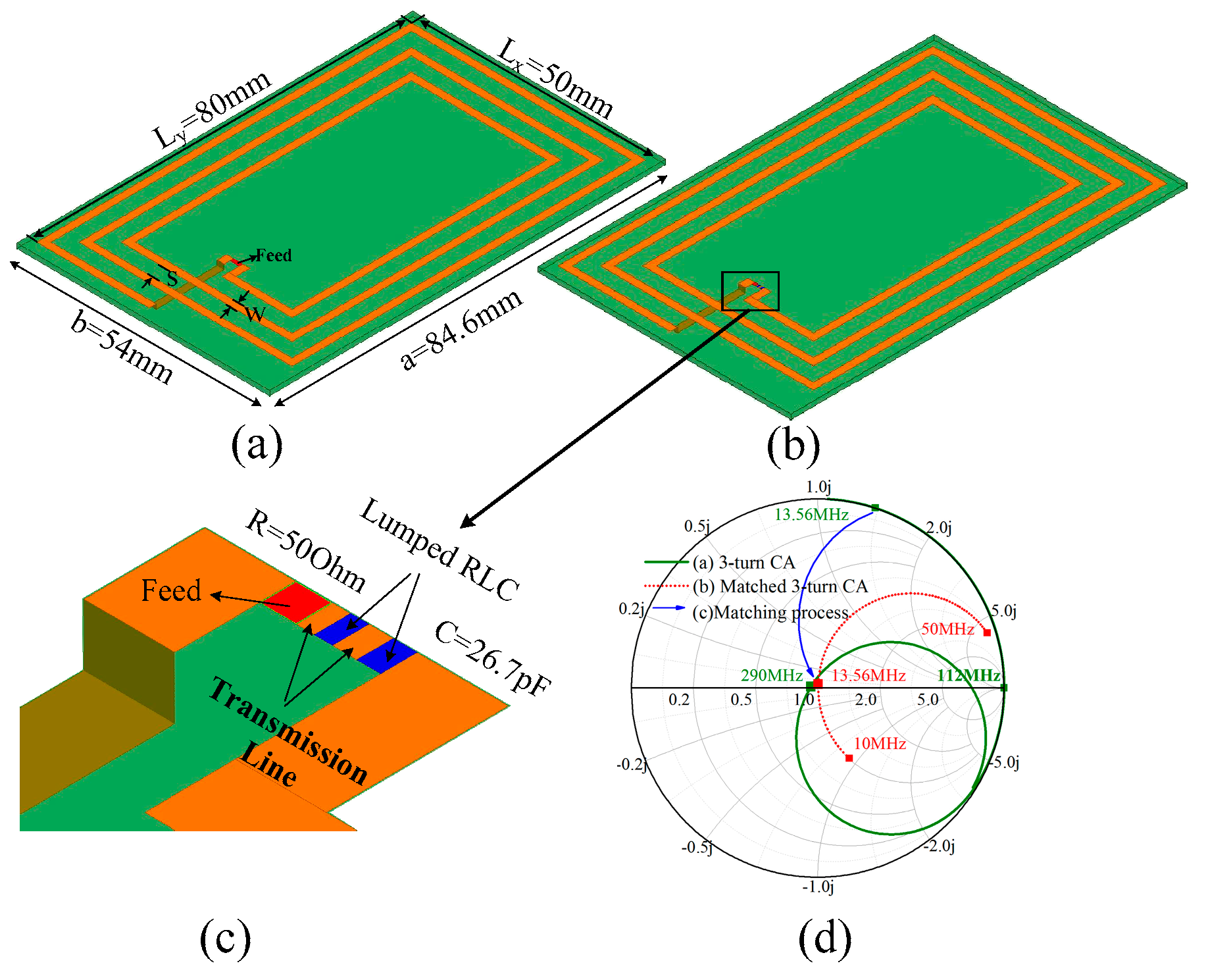
A near-field communication based on a coil antenna (CA) running at around 13.56 MHz frequency band is commonly used nowadays due to its easy integration, low cost and even operating without a network [1]. According to the inductive coupling, it can provide users with WPT mode to charge power and NFC mode to exchange information. Conventional handheld wireless devices based on a CA are bulky and multi-turn because of the limitation at the desired operational frequency band of 13.56 MHz [2]. However, the best reason for selecting the coil structure to be applied in a near-field situation is that power can be transmitted at high efficiency, regardless of alignment, by adjusting the magnitude and phase due to the eddy current generated along the multi-turn metallic coils. The issues of the body effect size reduction and bandwidth increases based on the CA; therefore, this has become a hot topic [3]. Simultaneously, with the demand for high-speed information exchange and limited by the crowding of handheld wireless devices, utilizing near-field interaction is more advantageous than using a SIM card [4,5,6,7]. Before some electronic components are integrated into a near-field wireless system, several related investigations into the dimension and turns of plane CA should be conducted to prevent the performance from degradation [8]. In most applied cases, CAs are integrated on the bottom of a battery pack, the thickness of which therefore must be taken good care of in design. However, the main aim of this paper is to miniaturize a CA based on a designed matching circuit. A 1-mm FR4 substrate is therefore taken to replace a battery pack in the following design. Meanwhile, a simple multi-turn CA is highly sensitive to alignment because of the narrow impedance bandwidth. If the dimension of the CA becomes smaller, it will be harder to maintain an original state of reflection coefficient at the desired frequency of 13.56 MHz, making it even more difficult to transmit power. Therefore, an approach to widening the impedance bandwidth also must be under consideration when miniaturizing a CA. Afterwards, the Q-factor determining the efficiency of transmitted energy is an important index for the whole RF system to be paid attention to, as fabricating a CA as small as possible with a high Q-factor is also necessary for wide impedance bandwidth [9]. The traditional approach to making the CA resonate at 13.56 MHz by simply cascading a resistance of 50 Ohm and a certain capacitance due to the standard impedance matching of 50 Ohm at the source port (as shown in Figure 1) was abandoned. However, it still has some reference values for following investigations and comparison due to its success in transmitting and receiving power at a certain frequency [10].
From its performance on the Smith chart in Figure 1d, the red dotted line and green solid line represent the S-parameter of a three-turn CA with and without a matching circuit, respectively. Simultaneously, the blue arrow line denotes the matching process of the desired frequency from the red dotted line to the green solid line at 13.56 MHz. The original three-turn CA denoted by the green line resonates at around 290 MHz, far away from the desired frequency of 13.56 MHz. However, this three-turn CA can finally operate at 13.56 MHz after cascading several electronic elements consisting of a resistance of 50 Ohm and a capacitance of 26.7 pF as shown in Figure 1b,c. Indeed, the conventional CA can operate at all frequencies desired by simply cascading a capacitor of a certain value and a 50 Ohm resistance because, according to the design specification of an RF system, there is a standard resistance of 50 Ohm matched at the feed port. Meanwhile, the CA itself has a particularly parasitic resistance whose value is rather small compared to the value of the feed port. Therefore, cascading a 50 Ohm resistor and a capacitor can easily make the CA resonate at around 13.56 MHz, ignoring the requirement of conjugate in the RF system. However this will definitely result in a considerable waste of source because most power will be consumed on heat by the resistor. The introduction of Q-factor can deal with this conventional problem with the best optimized performance achieved. For the above-discussed reasons, deigning a matching circuit with a suitable value of resistance is essential. To deal with this problem, a matching circuit based on electronic elements aimed at making a miniaturized CA scientifically operate at 13.56 MHz is designed [11]. Therefore, equivalent circuit parameter extraction and analysis of the CA is a necessary precondition before miniaturizing it.
The remainder of this paper is organized as follows: Section 2 introduces and interpret two approaches to miniaturizing the CA in theory. Two important RF modules to improve the performance of the CA are literally designed. Furthermore, two systematic design flows based on series and parallel equivalent circuits are presented in three steps. After designing the three-step flow for miniaturizing the CA in principle, this paper then provides two ways to check the results, namely, an electronic circuit and ANSYS, in Section 3. Finally, according to the concluded results, some further perspectives are presented in the last section.
2. Design of Miniaturization in Theory
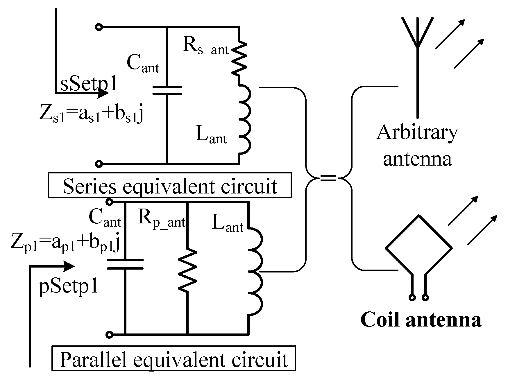
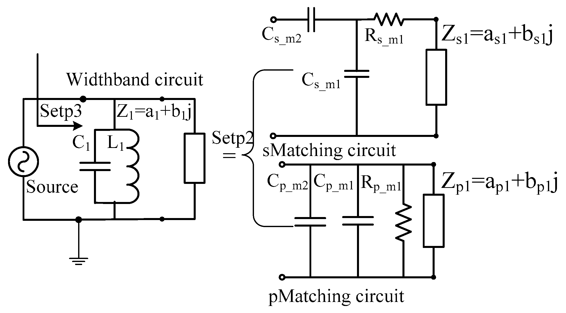
This section presents a complete design flow of miniaturizing a CA by way of an equivalent circuit in theory. An extracted equivalent circuit module can efficiently replace the antenna for calculation in an RF system due to the mature high-frequency electronic theory. Two approaches proposed in this paper to miniaturize the CA and widen the impedance bandwidth are based on this. Before designing a matching circuit for the CA, some rules and parameters influencing performance of an RF system should be introduced first. As shown in Figure 2, most antennas can be regarded as a radio-frequency circuit consisting of a capacitor, resistor and inductor, whose values can be extracted and calculated by HFSS software in simulation or by multimeter in measurement. Furthermore, these equivalent circuits can be divided into series equivalent circuits and parallel equivalent circuits according to their connections among electronic elements, as shown in Figure 2 for the following calculations [12].
The conventional CA’s inductance is about 1 to 2 uH, as it has 3-turn metallic loops and a 50 × 80-mm2 dimension, which can be regarded as a constraint condition to find an appropriate design specification in order to determine the miniaturized CA’s amount of turns. This is because either too large or too small inductance will deteriorate the performance of transfer. Therefore, if excellent performance in transferring power and information is required from the miniaturized CA, its inductance will be approximately equal to 1 to 2 uH, which is also key to miniaturizing a CA. In fact, the relationship among the inductance value and variable parameters of the CA can be formulated by the following equation, Equation (1) [13]:
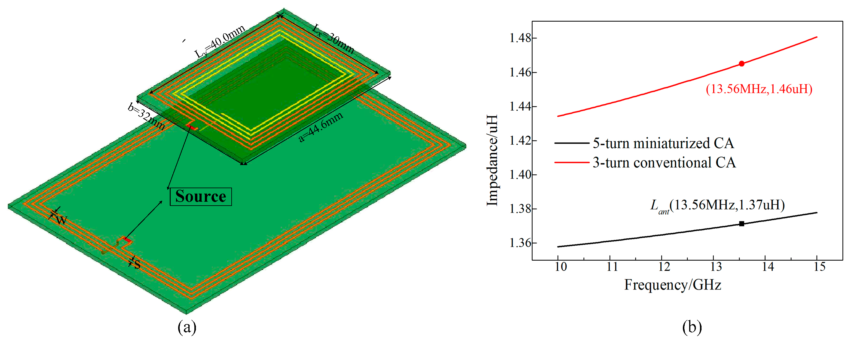
In this equation, dependent variable L whose unit is nH is an estimated value of the CA that can be approximately achieved by extracting parameters from the CA. The variables ly and Dx, corresponding to Figure 1a, represent the average perimeter and line width of a CA, respectively. Their unit is centimeter, and K is a constant with the value of 1.47 when the coil antenna is rectangle. If the CA is annular, the constant K is equal to 1.07. These are both obtained by empirical conclusion, which can be deemed suitable for designing coil antennas. The variable N denotes the turns of the CA. Therefore, if a size reduction is required for constant inductance, this equation should be made full use of. According to Equation (1), the inductance decreases due to the CA’s dimension reduction. Complying with the guide of inductance (Equation (1)), miniaturizing the CA will therefore reduce the value of Ly and Dx, causing a decrease in gross inductance. For the same performance as a conventional CA, some methods such as K reduction or N increase to maintain the inductance between 1 and 2 uH should be adopted. By analyzing the dynamic equation, Equation (1), increasing the variable N will play a more important role in maintaining its inductance than reducing the variable Dx or constant K. For an obviously effective result, this paper decides to keep the inductance constant by adding the turns of the CA. The inductances of a three-turn and five-turn CA are calculated and tabulated based on the dynamic equation, Equation (1), as shown in Table 1 (unit: nH).
According to Table 1, a conventional three-turn CA itself has an inductance of 1.68 uH, exactly located in the range of 1 to 2 uH. However, both inductances of four-turn and five-turn miniaturized CAs are within the desired range; the latter has the closer inductance to the conventional three-turn CA highlighted by bold font. The turns of the coil antenna are therefore determined to be five for its inductance named Lant being about 1.706 uH, meeting the requirement of design specification. Corresponding to Figure 2, CA’s equivalent resistance in the series mode named Rs_ant can be achieved by multimeter in measurement and by a software simulator in simulation. Furthermore, CA’s equivalent resistance in the parallel mode named Rp_ant can be achieved by the following equation, Equation (2) [14]:
In this equation, Rp_ant is the resistance in the parallel equivalent circuit at 13.56 MHz. Rp_self can be regarded as pure resistance when the initial CA only resonates at current frequency. On the right of the equation, ƒ(ant) and ƒ(self) are the frequencies of the desired and current state, respectively. Additionally, the capacitance of the miniaturized CA named Cant can be calculated by the LC equation, Equation (3)
In this equation, ƒ is the currently operational frequency and L is the inductance of the miniaturized CA. In this equivalent circuit, L = Lant. All their real values are given in the following section for calculation in simulation. Here, step one, parameter extraction of equivalent circuit, is complete.
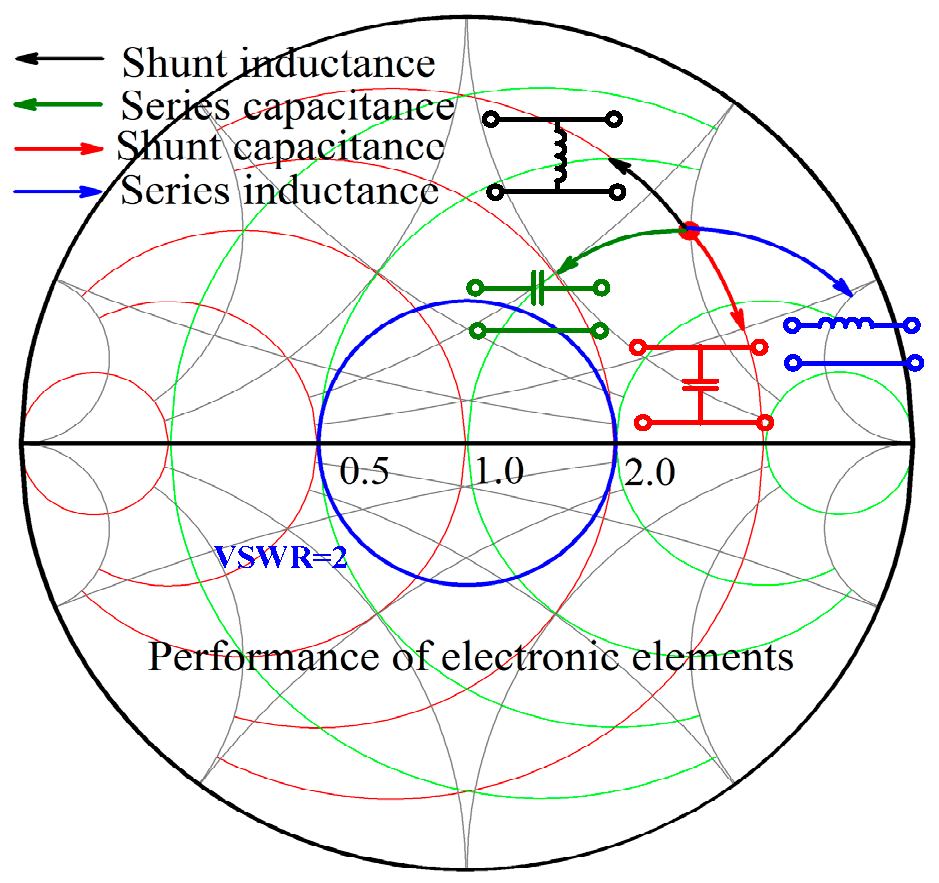
Additionally, an equivalent circuit of the CA can not solely resonate at the desired frequency of 13.56 MHz until a matching circuit is connected with it. Therefore, the characteristics of RF electronic elements should be investigated and calculated before they are adopted in a matching system. A Smith chart can visually present the influence of every electronic element on the equivalent circuits of the CA, as shown in Figure 3.
In the above Smith chart, a shunt and series capacitor and inductor can be found. Every electronic element has its own property on the electronic system when connected to it. Shunt inductance can make the currently operational point extracted from the CA move along the red circle anticlockwise, and the shunt capacitance can make the currently operational point move along the red circle clockwise. Similarly, series inductance denoted by the blue arrow line can make the currently operational point move along the green point clockwise, and the series capacitor can make the current operational point move along the green point anticlockwise. According to RF electronic circuit theory, every operational state of an extracted equivalent circuit can be mapped on the corresponding Smith chart. An excellently designed matching circuit should move the current operational point to the center of the circle, making the whole RF system resonate at a frequency of 13.56 MHz. Before deigning the matching circuit, an index, the Q-factor, should be selected carefully in different equivalent models, as it will have a great influence on the performance of the near-field wireless system. Here, suppose the Q-factor is equal to 10, meeting the requirement of industry specification ISO14443. Therefore, the gross resistance of matching and equivalent circuits in the series situation named Rs_tol can be calculated by Equation (4). Similarly, the gross resistance in the parallel situation named Rp_tol can be obtained by Equation (5).
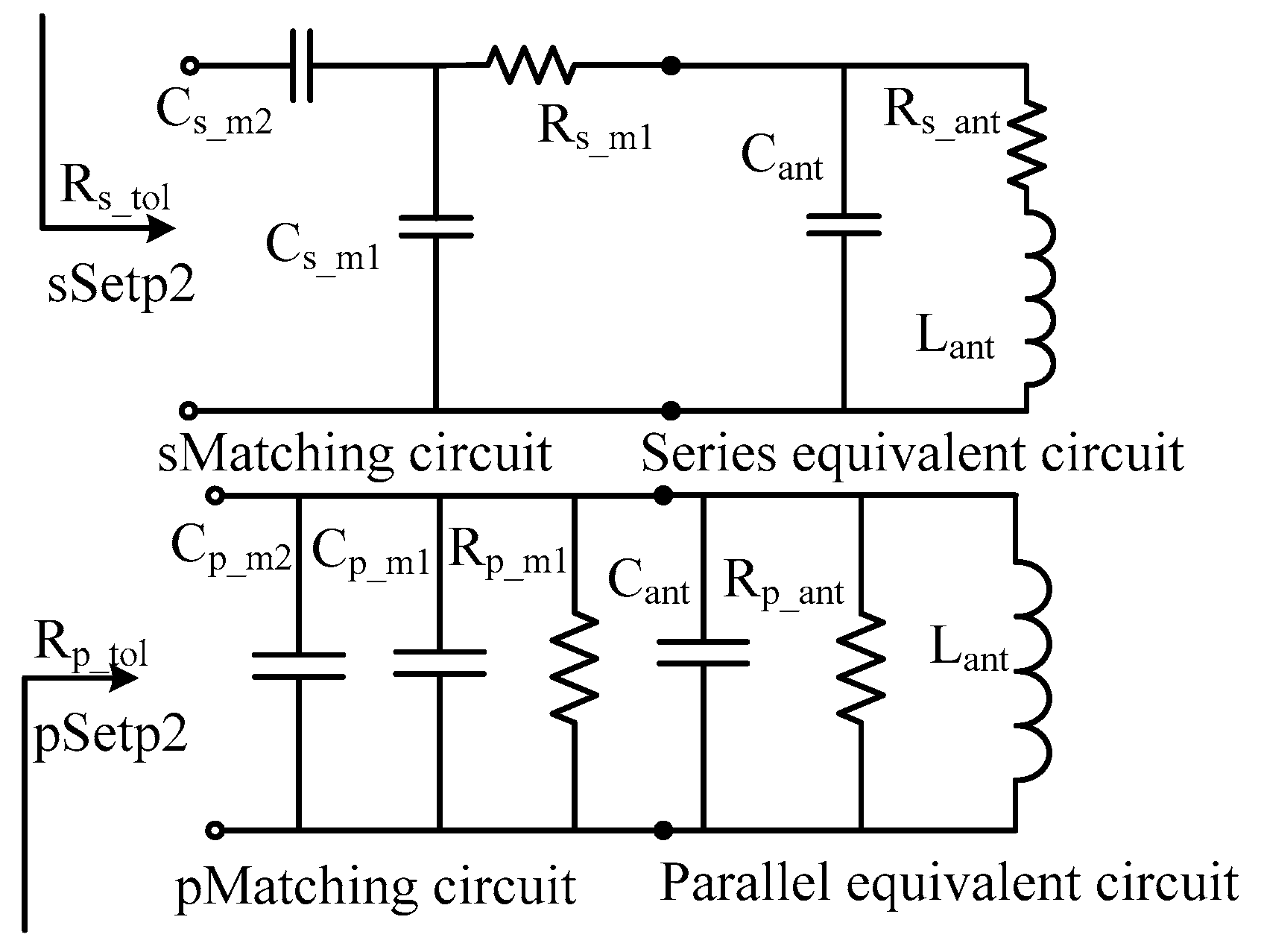
where the Rs_m1 and Rp_m1 are the resistances needed to be deployed in the matching circuit. The ω is the angular frequency at the best operational state. Here, ω is equal to 2π × 13.56 MHz. L is the value of inductance of the miniaturized CA at the same frequency. Furthermore, the respective values of Cs_m1 and Cs_m2 can be easily obtained based on Equation (6) due to the conjugate relation after normalization in the Smith chart [15].
According to the Smith chart, every value of matching electronic elements can be calculated easily, and the detailed process is presented in the following section. Similarly, the parallel matching circuit can be designed with the same process. Finally, the second step of the RF electronic system named the interim circuit is complete, and the matching circuits for the series and parallel equivalent circuits can be obtained, as shown in Figure 4.
However, according to existing literature, small antenna cannot obtain broad bandwidth unless some additional technologies are adopted. After integrating a matching circuit, an LC resonator must be introduced to the RF electronic system for a broader bandwidth as a third step. According to Equation (3), an LC resonator designed to exactly resonate at 13.56 MHz can efficiently widen the bandwidth according to RF electronic rules as seen in Figure 5. Moreover, small values of inductance and large values of capacitance have good performance in widening the impedance bandwidth at low frequency.
Several pairs of specific parameters of the LC resonator meeting the restriction of Equation (3) are listed in Table 2. After fine adjustment, the final data are determined by plotting the performance of the electronic elements on a Smith chart.
In summary, after miniaturizing the dimension of the CA, establishing an equivalent circuit according to extracted parameters from the miniaturized coil antenna is the first key step. Then, the second step is to design a specially matching circuit for the circuit achieved in the first step. Furthermore, an LC resonator operating at around 13.56 MHz is introduced for higher performance [16].
3. RF System Design and Verification in Simulation
Although the introduction of miniaturizing a CA based on theory is detailed enough, it cannot be verified unless some simulated experiments are conducted. Both series and parallel approaches are useful to miniaturize CA; for convenience, this section only takes the series equivalent circuit as an example to verify the proposed approach to miniaturizing the CA and further widen the impedance bandwidth. Therefore, the proposed approach to enhancing the performance of the miniaturized CA is simulated and assessed in ADS and ANSYS HFSS software one by one. Meanwhile, the parallel equivalent circuit of the CA can be matched to resonate at 13.56 MHz by a similar approach. The model of a five-turn miniaturized CA printed on a 1- mm FR4 substrate and simulated in HFSS software with the inductance of about 1.37 uH meeting the range requirement of about 1 to 2 uH verifies the inductance of Equation (1) in Section 2, as shown in Figure 6b. Figure 6 presents a comparison of inductance between three- and five- turn CAs within 10 to 15 MHz, covering the design specification of near-field wireless communication devices.
3.1. A Circuit Simulation Based on ADS
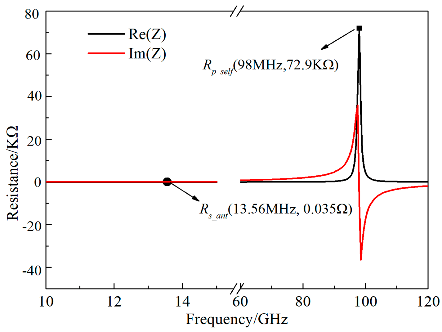
By calculating the extracted parameters from simulation, the impedance of Z’s real and imaginary part of the five-turn CA is plotted in Figure 7 to obtain the equivalent resistance, Rs_ant and Rp_ant, in different models in simulation. It is worth noting that the Rp_ant’s value of 27.117 KΩ can be achieved by transforming Equation (2) as shown in Equation (7). Otherwise, the Rs_ant can be directly obtained by the plotted impedance data, being 0.035 Ohm.
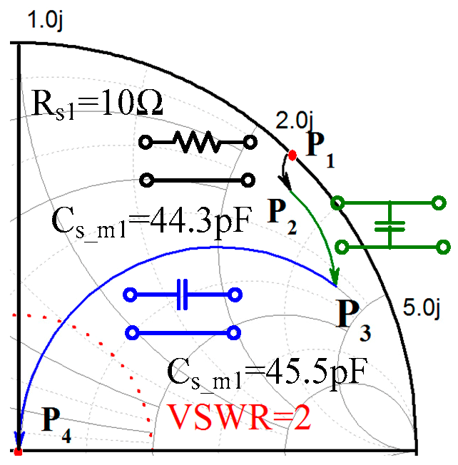
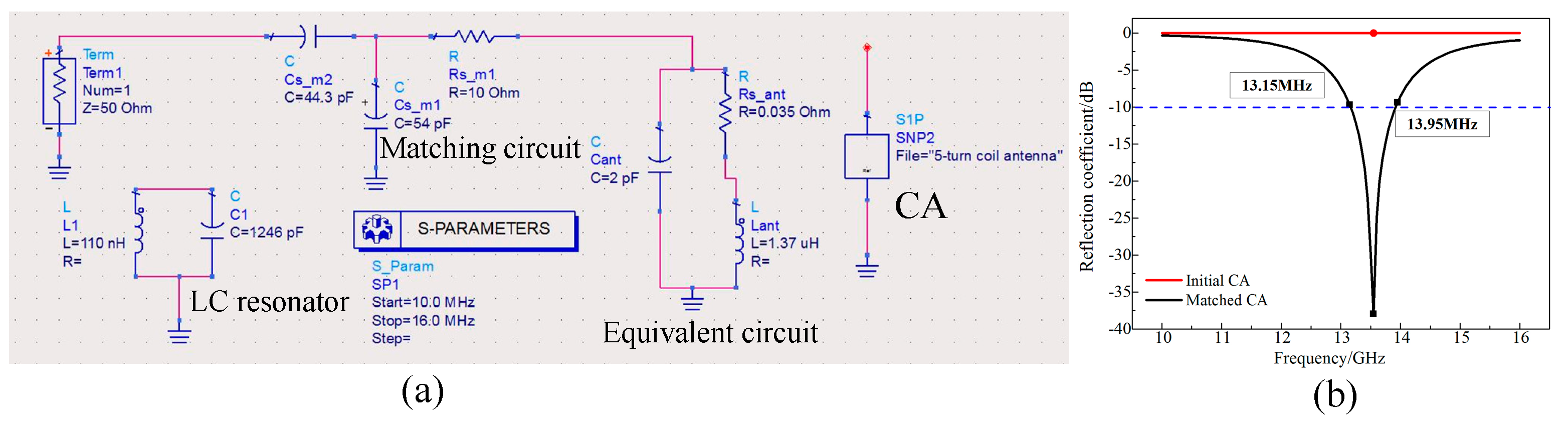
To calculate the respective gross resistance, Rp_tol and Rs_tol in step two for different equivalent models, the two above-mentioned resistance equations, Equations (4) and (5), based on Q-factor, are utilized here. Simultaneously, the inductance of the calculated five-turn CA is equal to 1.37 uH as shown in Figure 6. According to Equations (4) and (5), at the operational frequency of 13.56 MHz, the Rp_tol and Rs_tol are equal to 12 Ω and 1.17 KΩ, respectively. The Rs_m1 and Rp_m1 can therefore be derived by transforming the same equations, Equations (4) and (5). Finally, their values are approximately equal to 12 Ω and 1.22 KΩ, respectively. Complying with the performance of every electronic element discovered in Figure 3 in Section 2, every element desired can be found easily with the help of the Smith chart as shown in Figure 8. If the CA needs to operate at a desired band, certain traces should be selected to move the current state from P1 to P4 using the rules introduced in Section 2. Starting at the red point P1, which is the current state of the five-turn miniaturized CA, a resistance named Rs_m1 is cascaded, as shown in Figure 9a, making the point move from P1 to P2. Two capacitors named Cs_m1 and Cs_m2 are next connected to it, making the point P2 move to P4. Their respective values of 44.3 pF and 45.5 pF can be determined directly with the help of the Smith chart.
For verification, a matching circuit model with the values obtained from the previous Smith chart is established in ADS software, as shown in Figure 9a. Meanwhile, the simulated comparable results of the interim system with and without a matching circuit are plotted in Figure 9b; there is an obvious additional resonance at exactly 13.56 MHz compared to the equivalent circuit without a matching circuit. Therefore, this series equivalent circuit has a greater performance on this miniaturized CA.
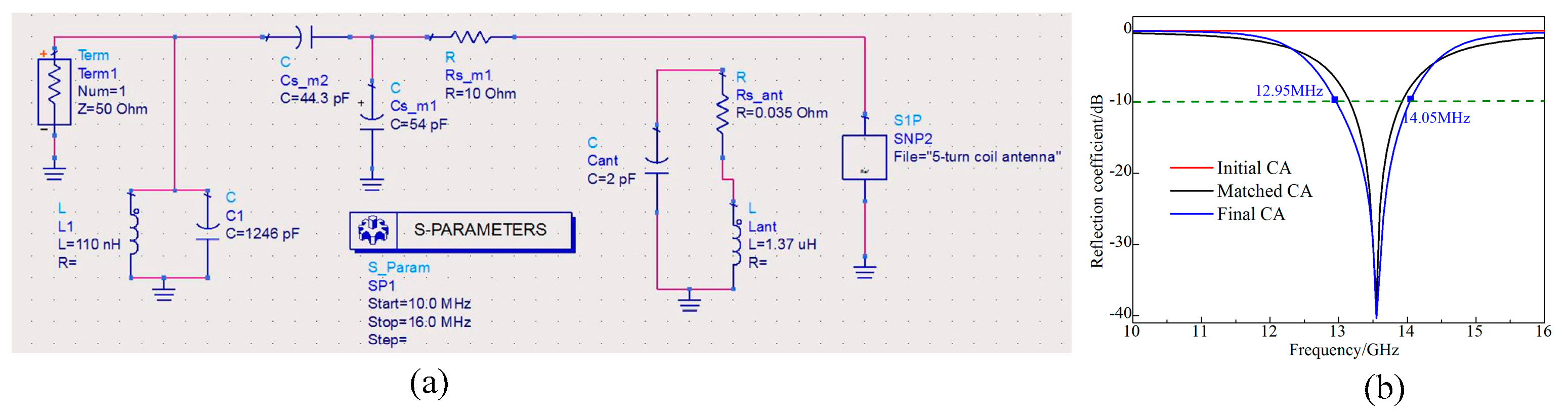
After extracting the equivalent circuit and designing the matching circuit for this five-turn miniaturized CA, a specially designed LC resonator can be introduced to further enhance the performance by widening the impedance bandwidth for the interim system, forming the final RF system as shown in Figure 10a. Meanwhile, Figure 10b shows the compared result using all of the steps discussed in the theory. The impedance bandwidth is clearly broader than the one without the LC resonator, enhancing the performance of the final system.
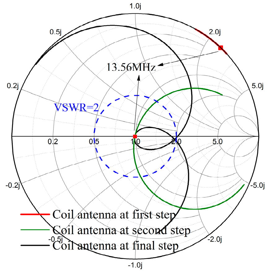
It can be verified from the figures above that the matching circuit and LC resonator play an important role in enhancing the performance of the CA. Figure 11 presents a clearer description of the optimizing process by plotting the operational state on the Smith chart. The red line denotes the operational state of the only miniaturized five-turn CA from 10 to 15 MHz, which is along the edge of the Smith chart, meaning a completely mismatching antenna. The green and black curve represent the matched and ultimate state of the miniaturized antenna, respectively. After two optimizations, their desired resonant points of 13.56 MHz are both located at the center of the Smith chart. However, the curve of final operational state becomes more twisted than that of the only matched CA, meaning more of a range is located in the blue dotted circle where the VSWR is equal to 2. This can therefore clearly interpret every module’s influence on the coil antenna in the whole system.
3.2. Model Simulation Based on ANSYSA
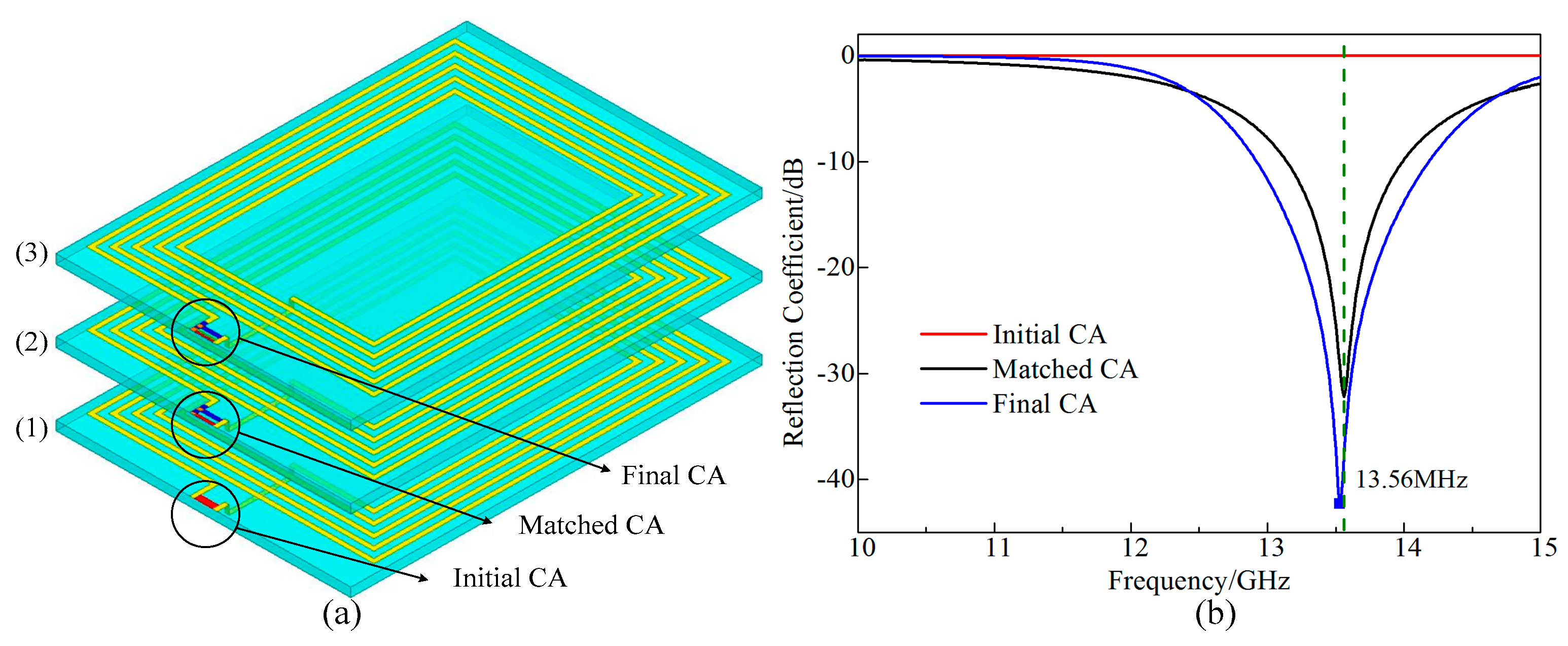
Concluded from the three steps of the Smith chart, there is an obvious difference among these circuits, verifying its validity in optimizing the equivalent circuit based on circuit analysis [17]. For a strong demonstration, another way based on ANSYS is adopted to assess the above-mentioned theory and simulation simultaneously. Here, an additional model established in ANSYS HFSS is utilized to test the proposed way to miniaturize the CA. The model is also a specialized EM simulator like ADS but based on ANSYS, which has been proved valid in RF fields [18]. It is worth noting that in ANSYS HFSS, the lumped port function can easily replace the RF electronic elements in ADS by several equivalent patches. Moreover, as shown in Figure 12, the substrates of CAs are all based on FR4, whose permittivity is 4.4 and thickness is only 1 mm. Furthermore, the function of Perfect E can be used on the coils to denote the metallic conditions. Finally, a large air box should contain all of the CAs with a radiation condition to simulate the air. Figure 12a presents three miniaturized CA models corresponding to the three steps discussed in Section 2. Figure 12a1 is a CA model without any electronic elements corresponding to a miniaturized CA without any electronic elements connected; Figure 12a2 is an interim model with a sole matching circuit, and Figure 12a3 denotes the ultimate model with a matching circuit to optimize the resonance band and LC resonator to widen the impedance bandwidth corresponding to the final system in step three. Their ports are deployed by different color patches representing various kinds of electronic elements. The red and orange patches in the three models represent the exciting sources and transmission line, respectively. Every blue patch denotes an electronic element; this may be a resistor, a capacitor or an inductor. Additionally, the green patch next to the red one in Figure 12a3 represents an integrated module; here, it is an LC resonator.
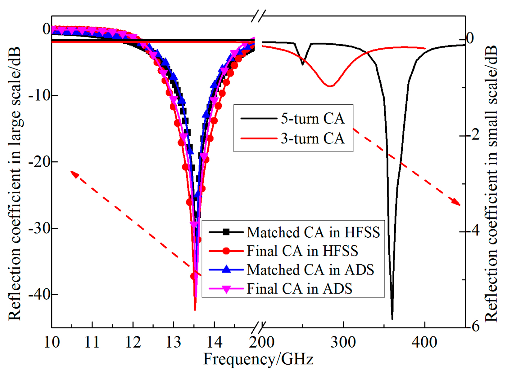
An intuitive comparison of the S-parameters among the three above-discussed models at around 13.56 MHz is presented in Figure 12b. There is also an obvious difference in the resonance band and impedance bandwidth. The interim-matched CA only has a stronger resonance at 13.56 MHz compared to the one without a matching circuit. Moreover, the ultimate RF system based on a matching circuit and LC resonator can not only resonate strongly in the desired band but also has a broader impedance bandwidth than the interim-matched CA. Finally, Figure 13 shows the comprehensive comparable results of different types of models in HFSS and ADS, both presenting good agreement with the proposed approach to miniaturizing a coil antenna in theory. The integrated circuit tech is already advanced enough to be applied in almost all electronic devices due to its mature theory. Therefore, two designed modules based on electronic elements can be integrated into the CA to improve the performance of each.
Comparing the reflection coefficients of the five-turn and three-turn Cas with the designed CA, there is an obviously frequency offset and performance improvement on resonant band, which is manipulated by the matching circuit. Therefore, the design of a miniaturized CA for NFC was successful.
3.3. WPT Verification
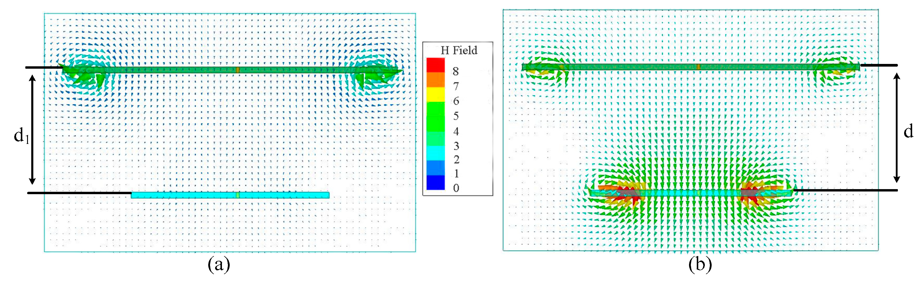
The CA’s characteristics were enhanced by integrating two proposed modules, making it efficiently radiate EM wave at 13.56 MHz to realize the function of NFC. Of course, this miniaturized coil antenna can also transfer power to a conventionally matched CA that simultaneously has the same resonant frequency. Observing the comparison in Figure 14, Figure 14a,b are two H-field distribution maps of two CAs of different sizes., In Figure 14a, the top coil antenna is a conventionally matched coil antenna operating at 13.56 MHz and the bottom one is a single miniaturized coil without designed modules. In Figure 14b, only the bottom one is replaced by an optimized miniaturized CA. According to this comparison described in HFSS, it can be found that the E field cannot be radiated from one coil antenna to the other one by the EM wave unless two CAs work at the same frequency. Indeed, there is a strong mutual coupling between two CAs operating at around 13.56 MHz, verifying that it is possible to successfully miniaturize a coil antenna according to the designed flow [19,20].
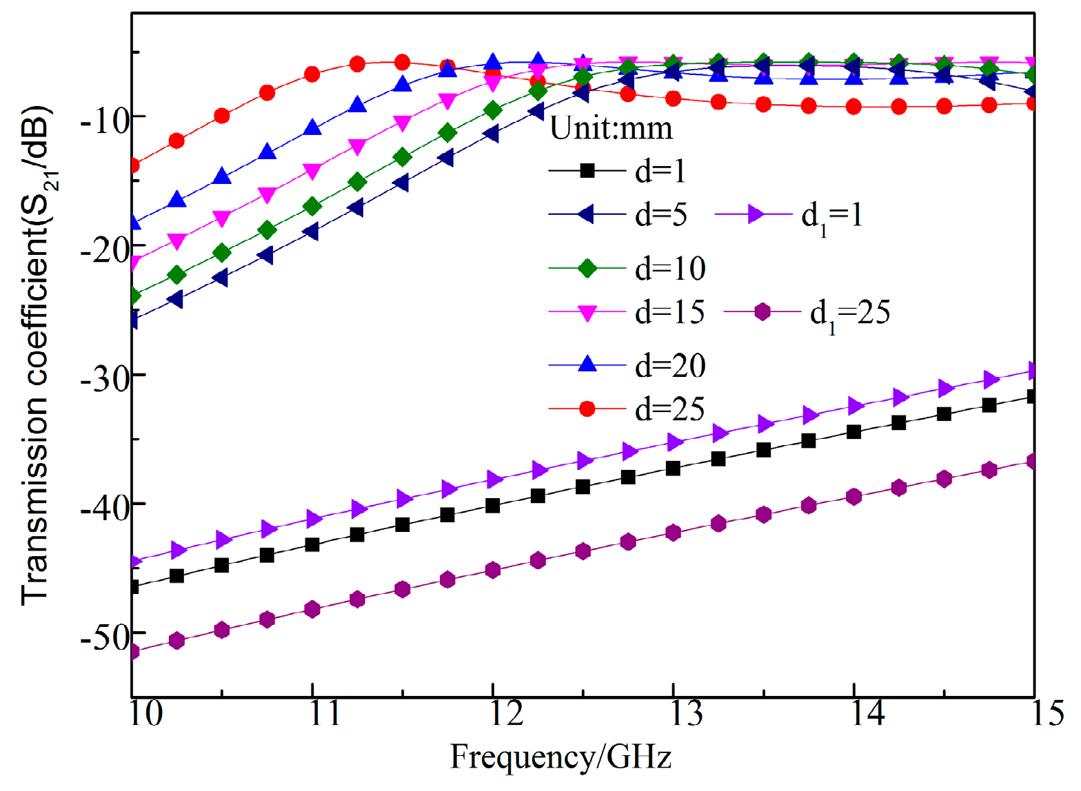
For more detailed results, a compassion between Figure 14a,b for various distances d is plotted in Figure 15. From this, it can be clearly seen that either too far or too short of a distance will deteriorate the transmitting performance between the two coil antennas. When the two coil antennas get too close to each other, they can be regarded as extra inductance to each other, destroying the balance of resonance. Meanwhile, when the distance d becomes too long, the energy will be transmitted poorly due to the loss of air.
4. Conclusions
A complete method of miniaturizing a CA at a frequency of 13.56 MHz is proposed and verified based on detailed data in this paper. Several basic theories based on RF electronic circuits are applied to optimize the miniaturized CA and achieve satisfactory results. Meanwhile, a circuit model and prototype model are established and present good agreement in ADS and ANSYS HFSS. Both of the models also present outstanding performances with the help of a matching circuit and LC resonator. Meanwhile, the CA’s dimension can be reduced from 400 mm2 to 120 mm2 (shrinking by 70%), and its impedance bandwidth widened from 0.8 to 1.1 MHz (increasing by approximately 40%). Therefore, the novel method proposed in this paper can provide new guidance regarding miniaturized RF circuits that achieve improved performances.
Author Contributions
Conceptualization, Z.D. and Z.Z.; Investigation, X.Y. All authors have read and agreed to the published version of the manuscript.
Funding
This research received no external funding.
Conflicts of Interest
The authors declare no conflict of interest.
References
- Curran, K.; Millar, A.; Garvey, C.M. Near field communication. Int. J. Electr. Comput. Eng. 2012, 2, 371–382. [Google Scholar] [CrossRef]
- Lee, B.; Kim, B.; Harackiewicz, F.J.; Mun, B.; Lee, H. NFC Antenna Design for Low-Permeability Ferromagnetic Material. IEEE Antennas Wirel. Propag. Lett. 2014, 13, 59–62. [Google Scholar]
- Benavides, M.; Miralles, D.; Andújar, A.; Anguera, J. Effects on human body and conductive body over a near field communication antenna. J. Electromagn. Waves Appl. 2021. [Google Scholar] [CrossRef]
- Li, R.L.; De Jean, G.; Laskar, J.; Tentzeris, M.M. Investigation of circularly polarized loop antennas with a parasitic element for bandwidth enhancement. IEEE Trans. Antennas Propag. 2005, 53, 3930–3939. [Google Scholar]
- Want, R. An introduction to RFID technology. IEEE Pervasive Comput. 2006, 5, 25–33. [Google Scholar] [CrossRef]
- Chen, W.S.; Chang, P.C.; Chiu, T.W.; Hsiao, F.R. An embedded tri-band plan-ar inverted-F antenna with a branch-line shorting strip. IEEE Antennas Propag. Soc. Int. Symp. 2005, 18, 447–450. [Google Scholar]
- Hu, J.; Zhao, J.; Cui, C. A Wide Charging Range Wireless Power Transfer Control System With Harmonic Current to Estimate the Coupling Coefficient. IEEE Trans. Power Electron. 2021, 36, 5082–5094. [Google Scholar] [CrossRef]
- Bauernfeind, T.; Renhart, W.; Schemthanner, S. Equivalent circuit parameter extraction for controlled detuned NFC antenna systems utilizing thin ferrite foils. In Proceedings of the 12th International Conference on Telecommunications, Zagreb, Croatia, 26–28 June 2013; pp. 251–256. [Google Scholar]
- Markish, O.; Leviatan, Y. Quality factor and absorption bandwidth of electrically small lossy structures. IET Microw. Antennas Propag. 2020, 14, 101–108. [Google Scholar] [CrossRef]
- Byungje, L.; Byeongkwan, K.; Sunghyun, Y. Enhanced Loop Structure of NFC Antenna for Mobile Handset Applications. Int. J. Antennas Propag. 2014, 2014, 187029. [Google Scholar] [CrossRef] [Green Version]
- Li, L.; Gao, Z.; Wang, Y. NFC antenna research and a simple impedance matching method. In Proceedings of the 2011 International Conference on Electronic & Mechanical Engineering and Information Technology, Harbin, China, 12–14 August 2011; pp. 3968–3972. [Google Scholar] [CrossRef]
- Lee, W.S.; Kim, D.Z.; Yu, J.W. Multi-functional high-isolation dual antenna for controllable wireless charging and NFC communication. Electron. Lett. 2014, 50, 912–913. [Google Scholar] [CrossRef]
- Mohan, S.S.; Hershenson, M.M.; Lee, T.H. Simple Accurate Expression for Planar Spiral Inductances. IEEE J. Solid State circuits 1999, 34, 1419–1424. [Google Scholar] [CrossRef] [Green Version]
- Li, Y.; Deng, S.; Zhang, Y. Coordinating the retail supply chain with item-level rfid and excess inventory under a revenue-cost-sharing contract. Int. Trans. Oper. Res. 2021, 28, 1505–1525. [Google Scholar] [CrossRef]
- Gunes, F.; Cetiner, B.A. Smith chart formulation of performance characterisation for a microwave transistor. IEE Proc. Circuits Devices Syst. 1998, 145, 419–428. [Google Scholar] [CrossRef] [Green Version]
- Zhang, W.; Yuandan, D.; Tatsuo, I. Metamaterial-based, miniaturised circularly polarised antennas for RFID application. IET Micro. Ant. Propag. 2020, 15, 547–559. [Google Scholar] [CrossRef]
- Lulu, X.; Xiao, C.; Sirui, T. Characterization and Modeling of Embroidered NFC Coil Antennas for Wearable Applications. IEEE Sens. J. 2020, 20, 14501–14513. [Google Scholar] [CrossRef]
- Chun, J.Y.; Noh, G. Privacy-Preserving RFID-Based Search System. Electronics 2021, 10, 599. [Google Scholar] [CrossRef]
- Yi, Z.; Li, M.; Muneer, B.; He, G.; Yang, X.-X. Self-Resonant Antisymmetric Planar Coil for Compact Inductive Power Transfer System Avoiding Compensation Circuits. IEEE Trans. Power Electron. 2021, 36, 5121–5134. [Google Scholar] [CrossRef]
- Zannas, K.; Matbouly, H.E.; Duroc, Y.; Tedjini, S. A Flipping UHF RFID Sensor-Tag for Metallic Environment Compliant With ETSI/FCC Bands. IEEE Trans. Antennas Propag. 2021, 69, 1283–1292. [Google Scholar] [CrossRef]
Figure 1.
A simple 3-turn CA (a) without matching circuit, (b) with an obsolete matching circuit (c); zoom-in of the schematic of matching circuit in simulation; (d) their s-parameters on Smith chart.
Figure 1.
A simple 3-turn CA (a) without matching circuit, (b) with an obsolete matching circuit (c); zoom-in of the schematic of matching circuit in simulation; (d) their s-parameters on Smith chart.

Figure 2.
Equivalent circuit models for general antennas.

Figure 3.
Performance of electronic elements on a Smith chart.

Figure 4.
The interim circuit consisting of equivalent and matching circuits.

Figure 5.
An LC resonator for the second-step electronic circuit.

Figure 6.
A comparison between three- and five-turn CA in simulation; (a) perspective geometry; (b) values of inductance.
Figure 6.
A comparison between three- and five-turn CA in simulation; (a) perspective geometry; (b) values of inductance.

Figure 7.
The real and imaginary part of Z parameter.

Figure 8.
Matching process for series equivalent circuit.

Figure 9.
(a) The model of interim circuit; (b) S-parameters of equivalent circuit and interim circuit.
Figure 9.
(a) The model of interim circuit; (b) S-parameters of equivalent circuit and interim circuit.

Figure 10.
(a) The model of ultimate circuit; (b) S-parameters of all circuits in 3 steps.

Figure 11.
The final state of interim and ultimate systems on the Smith chart.

Figure 12.
(a) A sandwich model presenting the evolution of miniaturizing coil antenna; (b) comparison of S-parameters.
Figure 12.
(a) A sandwich model presenting the evolution of miniaturizing coil antenna; (b) comparison of S-parameters.

Figure 13.
Reflection coefficients of all above−discussed CAs.

Figure 14.
Reflection coefficients of all above-discussed CAs. (a) the top coil antenna is a conventionally matched coil antenna operating; (b) only the bottom one is replaced by an optimized miniaturized CA.
Figure 14.
Reflection coefficients of all above-discussed CAs. (a) the top coil antenna is a conventionally matched coil antenna operating; (b) only the bottom one is replaced by an optimized miniaturized CA.

Figure 15.
Transmission coefficient of Cas for various distances.


Table 1.
The inductance of conventional and miniaturized CAs based on variable turns.
| Size (mm) Turns | 1 | 2 | 3 | 4 | 5 |
|---|---|---|---|---|---|
| Conventional CA (50 × 80) | 232.6 | 809.9 | 1680 | 2820 | |
| Miniaturized CA (30 × 40) | 384.2 | 753 | 1188 | 1706 |
Table 2.
Possible values of inductance and capacitance.
| L1 (nH) | 1 | 100 | 370 | 1000 | 1.379 × 10⁵ |
| C1 (pF) | 1.379 × 10⁵ | 1.379 × 10³ | 370 | 137.9 | 1 |
Publisher’s Note: MDPI stays neutral with regard to jurisdictional claims in published maps and institutional affiliations. |
© 2021 by the authors. Licensee MDPI, Basel, Switzerland. This article is an open access article distributed under the terms and conditions of the Creative Commons Attribution (CC BY) license (https://creativecommons.org/licenses/by/4.0/).
Share and Cite
MDPI and ACS Style
Yang, X.; Ding, Z.; Zhang, Z. A Complete Flow of Miniaturizing Coil Antennas Based on Matching Circuit. Electronics 2021, 10, 1159. https://doi.org/10.3390/electronics10101159
AMA Style
Yang X, Ding Z, Zhang Z. A Complete Flow of Miniaturizing Coil Antennas Based on Matching Circuit. Electronics. 2021; 10(10):1159. https://doi.org/10.3390/electronics10101159
Chicago/Turabian StyleYang, Xiaokun, Zhao Ding, and Zhengping Zhang. 2021. "A Complete Flow of Miniaturizing Coil Antennas Based on Matching Circuit" Electronics 10, no. 10: 1159. https://doi.org/10.3390/electronics10101159
Note that from the first issue of 2016, this journal uses article numbers instead of page numbers. See further details here.