
Hybrid Cross Coupled Differential Pair and Colpitts Quadrature Digitally Controlled Oscillator Architecture


Institute of Microelectronics and Optoelectronics, Warsaw University of Technology, ul. Koszykowa 75, 00-662 Warsaw, Poland
*
Author to whom correspondence should be addressed.
Electronics 2021, 10(10), 1132; https://doi.org/10.3390/electronics10101132
Submission received: 14 April 2021
/
Revised: 1 May 2021
/
Accepted: 7 May 2021
/
Published: 11 May 2021
(This article belongs to the Special Issue RF/Mm-Wave Circuits Design and Applications)
Abstract
:Growing importance of wireless communication systems forces reduction of power consumption of the designed integrated circuits. The paper focuses on minimization of power consumption in a digitally controlled oscillator (DCO) that can be employed as oscillator in GPS/Galileo receiver. The new hybrid architecture of DCO combines good phase noise performance of a Colpitts oscillator and relaxed startup conditions of a cross-coupled differential pair oscillator. The proposed new DCO generates a quadrature signal in a current reused frequency divider. Such solution allows of the dissipated power to be reduced. The DCO has been implemented in 110 nm CMOS technology. It generates output signal in frequency range from 1.52 GHz to 1.6 GHz and consumes 1.1 mW from 1.5 V supply voltage. The measured phase noise equals −116 dBc/Hz at 1 MHz offset from 1.575 GHz output signal.
1. Introduction
The digitally controlled oscillator is an important part of the All Digital Phase Locked Loop (ADPLL) employed as a Local Oscillator (LO) in integrated transceivers. The DCO is responsible for the generation of the radio frequency (RF) signal that is served to the mixer input in order to convert frequency. The most crucial parameters of the DCO are the frequency sweep range and phase noise of the generated signal, as well as the power consumption and occupied area.
ADPLL is a type of Phase Locked Loop (PLL) where some operations are performed in the digital domain instead of in the analog one [1]. One of the strongest advantages of ADPLL is the implementation of the loop filter in a digital manner making capacitors obsolete. Consequently, an ADPLL occupies less area than an analog PLL. Additionally, a digital loop filter improves the flexibility of loop bandwidth control. Moreover, ADPLL is easier to implement in a highly scaled CMOS technology [1].
Development of low power and highly integrated transceivers is one of the goals in modern wireless communication systems. Widespread use of mobile devices requires significant minimization of power consumption of the developed circuits. Extensive research has been carried out in order to minimize the dissipated power in wireless transceivers [2,3,4].
The oscillator is responsible for a big part of transceiver dissipated power. Therefore, minimization of the power consumed by the oscillator is one of the most important issues. There are two types of oscillators that are widely implemented in integrated circuits: ring oscillators and LC tank oscillators. Ring oscillators occupy less area in comparison with LC tank oscillators, because inductance in integrated circuits has large dimensions. However, LC tank oscillators have better phase noise performance [5]. Since phase noise is an important parameter in the GPS/Galileo application, the LC oscillator has been implemented in RF frequency synthesizer in GPS/Galileo receiver [6]. There are several ways to reduce the consumed power in an oscillator. In reference [7] a study of a current reuse generator was presented, a quadrature oscillator stacked with a divide-by-2 quadrature frequency divider circuit was described in [8], while [9] presents a gm enhanced oscillator. The quadrature DCO (QDCO) architecture presented in this paper combines two oscillator architectures, i.e., the Colpitts architecture and the cross coupled pair architecture.
Knowing the importance of energy saving in wireless integrated systems the main goal of this work is to develop a new QDCO architecture that meets the Global Positioning System (GPS)/Galileo specification [3] and consumes less power than other oscillators presented in the literature. The GPS/Galileo requirements for a frequency synthesizer are described in Table 1. The GPS system is different from other communication systems because it has only one receive channel and no adjacent channels [3].
2. Novel Hybrid DCO Architecture
The DCO is an important part of the ADPLL. It determines the frequency range of the output signal and the phase noise spectral density for frequencies above the ADPLL bandwidth. Additionally, it is the most power consuming part of the frequency synthesizer. The new hybrid architecture was designed in such a way that it combines the advantages of two popular LC oscillators, the cross coupled pair and Colpitts ones. Figure 1 shows a model of the designed hybrid oscillator. It consists of a Colpitts oscillator in gate-source feedback gm-boosted architecture [10], connected in parallel to a cross coupled pair oscillator and a divide-by-2 quadrature frequency divider. This solution aims to achieve GPS/Galileo specification with lower bias current in comparison to other oscillator architectures.
2.1. Negative Conductance Implementation
In the LC tank oscillator, oscillation starts when the negative conductance of the active device in the circuit is higher than the loss conductance of the LC tank [5]. There are a few LC tank oscillator architectures described in the literature. The most common is the cross coupled differential pair oscillator, because of simple architecture and its differential nature [5,11]. Another popular oscillator design is the Colpitts architecture. The Colpitts oscillator was originally developed as a single ended generator. However, differential signal is required in many communication systems. Therefore, nowadays the Colpitts oscillator is widely implemented in differential architectures. The Colpitts oscillator provides good phase noise performance and requires lower supply voltage in comparison to the cross coupled pair circuit. However, it requires higher power consumption to guarantee the appropriate startup condition [7]. To relax the startup condition, the basic Colpitts architecture is modified. The Authors of [9] present a gm-boosted Colpitts architecture, where an additional transistor pair was added to the typical differential Colpitts architecture. A gm-boosted Colpitts oscillator was used to develop the novel hybrid architecture of DCO. A schematic of the Colpitts oscillator constituting a part of the proposed hybrid oscillator was presented in Figure 2. Capacitors C3 and C4 are added to this architecture to reduce the Miller effect of the Cgd of NM1 and NM2 transistors [8]. Figure 3 shows a small signal model of the gm-boosted Colpitts oscillator. The small-signal negative conductance can be calculated as [10]:
where gm1 is the transconductance of transistors NM1 and NM2, and gm3 is the transconductance of transistors NM3 and NM4.
Apart from the Collpits oscillator, the negative conductance of the presented hybrid DCO architecture is implemented also by the cross coupled pair generator. This oscillator is connected in parallel to the LC tank as depicted in Figure 1 and its electrical schematic is presented in Figure 4. The negative conductance from the cross coupled pair architecture (gmCC) is connected in parallel to the oscillator tank. Consequently, gmCC is added to the transconductance of the active part of the Colpitts oscillator and then the small-signal negative conductance equals:
While gmCC equals [5]:
where gmNM5 is the transconductance of transistors NM5 and NM6 and gmNP1 is the transconductance of transistors PM1 and PM2.
This additional conductance relaxes the startup condition of the Colpitts oscillator. The oscillations are induced with lower bias current and consequently the power dissipated by the oscillator decreases (this is discussed further in Section 3). LC tank bias in presented hybrid oscillator is forced by voltage on PM1 and PM2 gates as depicted in Figure 4.
Figure 5 compares the conductance of the active parts of the gm-boosted Colpitts oscillator and the designed hybrid oscillator. The conductance was calculated using Equations (1) and (2) assuming that the bias current was 1 mA. In the hybrid oscillator the bias current was divided between the Colpitts oscillator part and the cross coupled part in different proportions. The current biasing the Colpitts part of the hybrid oscillator must be high enough to bias the divide-by-2 quadrature frequency divider and maintain a low spectral density of the phase noise of the generated signal which is the advantage of the Colpitts oscillator. The results show that the conductance in the hybrid oscillator is higher than that in the gm-boosted Colpitts oscillator when biased by the same current.
2.2. Quadrature Signal Generation
The GPS/Galileo receiver requires a quadrature signal [12]. There are a few ways to achieve a quadrature signal in an oscillator output. The first solution is coupling two identical oscillators so that the phase difference between their output signals is 90 degrees [9]. However, this solution significantly increases the occupied area because it requires additional inductance on chip. Another solution, described in [13,14], is an implementation of poly phase filter to generate quadrature signal. This implementation suffers from variation of resistance and capacitance values in Process Corners and temperature. The third widely used solution is a divide-by-2 quadrature frequency divider added to oscillator [15].
A frequency divider occupies less area than an additional oscillator. Moreover, it can dissipate less power if it reuses the oscillator bias current. However, this solution has also some disadvantages, such as divider’s self-oscillation. In this work the divide-by-2 quadrature frequency divider was implemented to generate the quadrature signal. Therefore, the presented hybrid oscillator was developed to generate output signal at frequency two times higher than required. A schematic of the frequency divider was presented in Figure 6. The divide-by-2 quadrature frequency divider was stacked with the Colpitts oscillator. This was possible because the Colpitts architecture requires lower supply voltage. The circuit was implemented in Ultra Low Leakage (ULL) CMOS 110 nm technology. For these reasons the transistor threshold voltage is relatively high and it was impossible to stack the frequency divider with the cross coupled pair oscillator. Since the frequency divider reuses the oscillator bias current the dissipated power is reduced, which was the goal of this work.
2.3. Capacitor Bank
The frequency of the oscillator’s output signal depends on the input control signal that consists of a series of bits in the case of a DCO. Therefore, appropriate capacitor bank had to be designed to change the frequency with the required precision. Figure 7 presents a schematic of the capacitor bank controlling the frequency of the designed oscillator. The capacitor bank is divided into 3 parts:
- Coarse tuning capacitors.
- Fine tuning capacitors.
- Delta sigma capacitors.
The fine-tuning capacitor bank is controlled by a thermometer code signal and consists of 64 switched capacitor branches. The thermometer code is used here to limit the impact of local process variations between the individual capacitor branches. The fine-tuning bank determines the required frequency (1.5754 GHz) in spite of temperature variations. To obtain the required accuracy of the generated frequency it was necessary to develop a relatively small switched capacitance (simulations indicate a value of 200 aF to fulfill the GPS/Galileo requirements). There are many works done to study capacitance implementation in LC tank. The comparison of capacitor types in terms of their application in RF circuits was presented in [16]. Whereas in [17] authors present the analysis of the substrate capacity in the designed oscillator and its influence on the LC tank capacity. Unfortunately, the smallest capacitor available in the 110 nm Process Design Kit (PDK) is 51 fF. For this reason, in order to obtain capacitance change equal to 200 aF, it was necessary to design full custom switch capacitor, which was shown in Figure 8. The parasitic capacitance between metallization layers is used as a unit capacitor in the capacitor bank. The capacitance is changed from 840 aF to 1050 aF, which leads to frequency change of around 120 kHz. Simulation results of a single capacitor branch are presented in Figure 9.
The bank of delta sigma capacitors consists of 4 capacitor branches that are controlled by delta sigma modulator and enable further improvement of the frequency resolution. The bank of the coarse tuning capacitors is used to compensate global process variations and voltage variations. In this work the maximum supply voltage change was assumed to be ±10% of the typical value (150 mV). This capacitor bank is controlled by an 8-bit binary signal. Changing a single bit changes the capacitance by 6.7 fF, which corresponds to one half of the fine-tuning bank range. The presented capacitor bank makes it possible to generate the output signal with the required frequency in spite of process, voltage and temperature (PVT) variations. GPS/Galileo application does not require oscillator with wide tuning range, therefore presented capacitor bank was design in such a way to generate required frequency signal with minimum number of switch capacitors branches. Limited tuning range of DCO makes possible to use inductor with higher inductance value and higher quality factor, which resulting in easier startup condition for oscillator and better phase noise performance. Quality factor of inductor used in presented circuit equals approximately 10 in typical case.
3. Simulation Results
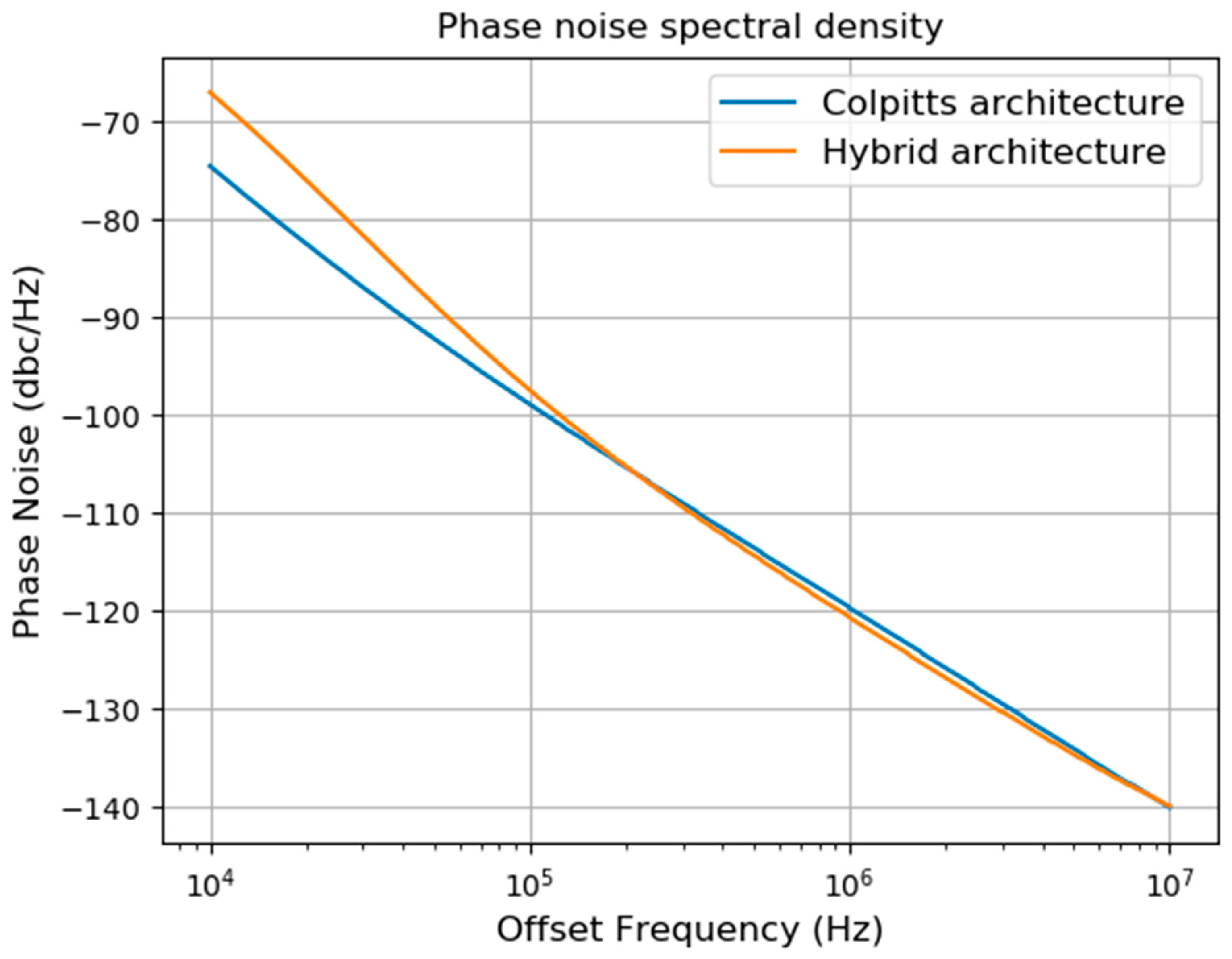
Transient simulations and phase noise simulations were carried out to determine the parameters of the developed hybrid DCO. The designed hybrid oscillator was compared to a gm-boosted Colpitts oscillator based on the architecture described in [8] and designed by the Authors of this paper specifically for the purposes of comparative analysis. Both oscillators were developed with the divide-by-2 quadrature frequency divider circuit in stack. The cross coupled differential pair oscillator was not compared with the other two, because it requires a higher supply voltage to stack it with a divide-by-2 quadrature frequency divider circuit. Both oscillators were simulated with 50 fF load on each output. This load is introduced by DCO buffer, which provides appropriate signal amplitude to the mixer input and drive frequency divider in feedback loop of ADPLL. The developed hybrid oscillator achieves reliable startup conditions at biasing current of 0.7 mA, while the gm-boosted Colpitts oscillator needs 1.4 mA. Figure 10 presents the startup time of each oscillator. The hybrid oscillator has shorter startup time and dissipates two times less power at the same time. Figure 11 shows the results of phase noise simulation for both circuits. Phase noise at 1 MHz from carrier frequency equals −120 dBc/Hz in each circuit. The new hybrid architecture has a higher 1/f phase noise spectral density than gm-boosted Colpitts architecture. However, it is not a disadvantage due to the high-pass characteristic of transmitting a DCO phase noise to the ADPLL output. A summary of the comparison between the gm-boosted Colpitts oscillator and hybrid oscillator is presented in Table 2.
4. Measurement Results
The developed hybrid oscillator was manufactured in Ultra Low Leakage 110 nm CMOS technology. Figure 12 presents a microphotograph of the fabricated circuit. Figure 13 and Figure 14 compare post-layout simulations and measurement results of the phase noise performance and frequency sweep range, respectively. Phase noise performance and frequency sweep range were measured by using Signal Source Analyzer (SSA) with 50 Ohm input load. In order to carry out measurements, output buffer based on common source amplifier architecture was designed to drive SSA input load.
Figure 13 shows differences between the measured and simulated phase noise performance. Presented phase noise performance results were measured and simulated for 1.574 GHz output frequency signal. For frequencies above 300 kHz from carrier signal, the measured phase noise spectral density is 2 dBc/Hz higher than simulated. This inaccuracy may result from process variations. The difference in phase noise performance for signals with carrier frequency offset less than 300 kHz is more significant, which is most likely due to imperfections in 1/f noise modeling in the PDK. Problems with 1/f noise modeling were observed also in other circuits on chip. Despite the difference between simulations and measurements results concerning phase noise spectral density at frequencies close to carrier, the designed oscillator fulfills the GPS/Galileo specification, because this low-band noise will be filtered by the ADPLL.
The measured frequency sweep range of the manufactured oscillator is close to the simulations results. Measurement results prove that the developed switched capacitors branches work as intended. The difference between the measured and simulated output signal frequency could be caused by process variations, however the oscillator was designed to fulfill the GPS/Galileo specification in spite of process variations. Measurement results confirm that the DCO parameters are situated between extreme results of process corner simulations.
5. Conclusions
A novel hybrid digitally controlled oscillator combining the architectures of the cross coupled pair and Colpitts oscillators was designed. The presented oscillator achieves the aim of this work, which was to develop an oscillator for a GPS/Galileo receiver and reduce the oscillator’s power consumption below the values presented in the literature.
The novel hybrid architecture combines the advantages of the cross coupled pair and Colpitts architectures. The cross coupled transistor pair enables reliable startup to be achieved at a lower bias current in comparison to the Colpitts architecture. On the other hand, the Colpitts oscillator has a good phase noise performance and requires lower supply voltage, which makes it possible to add a divide-by-2 quadrature frequency divider stacked with the oscillator. Such a divider generates a quadrature signal without consuming additional current from the supply.
The presented hybrid oscillator meets the GPS/Galileo specification. It generates a quadrature signal at frequency of 1.52–1.60 GHz and dissipates 1.1 mW power. The spectral density of phase noise at 1 MHz from carrier frequency equals −116 dBc/Hz.
Table 3 compares the developed circuit to other circuits described in the literature. Even though the Figure of Merit (FOM) does not show the superiority of the presented DCO architecture over other circuits presented in the literature the hybrid system has the lowest power consumption and occupies the smallest area. Moreover, the presented oscillator was designed in aluminum CMOS 110 nm ULL technology. Aluminum metallization layers have higher resistance compared to copper connections, which causes a significant degradation of the LC tank quality factor. Thus the proposed hybrid architecture obtains a comparable FOM using an aluminum technology with the added bonus of occupying a small area. This can be important, especially in commercial applications, as very often aluminum metal stack is used to reduce the fabrication cost. Small chip area is also desirable from the cost perspective.
The presented comparison shows that a hybrid of cross coupled pair and Colpitts digitally controlled oscillator reduces the required bias current. The presented novel architecture could facilitate the reduction of the power consumed in oscillators designed for other applications.
Figure of Merit was calculated based on the following equation:
where is offset frquency from carrier, is phase noise spectral density at , is oscillator output signal frequency and is oscillator disipated power.
Author Contributions
The work presented in this paper was a collaboration of all authors. RF and analog design, visualization, writing, I.B.; conceptualization, validation and RF design, K.S.; supervision, writing—review and editing, project administration, funding acquisition, W.A.P. All authors have read and agreed to the published version of the manuscript.
Funding
This work was supported in part by the Polish National Centre for Research and Development under project No. POIR.04.01.04-00-0101/16.
Data Availability Statement
The data presented in this study are available on request from the corresponding author. The data are not publicly available due to the ongoing project restrictions.
Conflicts of Interest
The authors declare no conflict of interest.
References
- Staszewski, R.B. State-of-the-art and future directions of high-performance all-digital frequency synthesis in nanometer CMOS. In Proceedings of the 2010 IEEE International Symposium on Circuits and Systems, Paris, France, 30 May–2 June 2010; pp. 1497–1510. [Google Scholar]
- Steyaen, M.S.J.; De Mueer, B.; Leroux, P.; Bommans, M.; Menens, K. Low-voltage low power CMOS-RF transceiver design. IEEE Trans. Microw. Theory Tech. 2002, 41, 281–287. [Google Scholar]
- Cheng, K.-W.; Natarajan, K.; Allstot, D.J. A Current Reuse Quadrature GPS Receiver in 0.13μm CMOS. IEEE J. Solid-State Circuits 2010, 45, 510–523. [Google Scholar] [CrossRef]
- Liscidini, A.; Mazzanti, A.; Tonietto, R.; Vandi, L.; Andreani, P. Single-Stage Low-Power Quadrature RF Receiver Front-End: The LMV Cell. IEEE J. Solid-State Circuits 2006, 41, 2832–2841. [Google Scholar] [CrossRef]
- Ham, D.; Hajimiri, A. Concepts and methods in optimization of integrated LC VCOs. IEEE J. Solid-State Circuits 2001, 36, 896–909. [Google Scholar] [CrossRef] [Green Version]
- Borejko, T.; Marcinek, K.; Siwiec, K.; Narczyk, P.; Borkowski, A.; Butryn, I.; Łuczyk, A.; Pietroń, D.; Plasota, M.; Reszewicz, S.; et al. NaviSoC: High-Accuracy Low-Power GNSS SoC with an Integrated Application Processor. Sensors 2020, 20, 1069. [Google Scholar] [CrossRef] [PubMed] [Green Version]
- Cheng, K.-W.; Chang, S.-K.; Huang, Y.-C. Low-Power and Low-Phase-Noise Gm-Enhanced Current-Reuse Differential Colpitts VCO. IEEE Trans. Circuits Syst. II Express Briefs 2019, 66, 733–737. [Google Scholar] [CrossRef]
- Ji, X.; Wu, J.; Shi, L. Current reused Colpitts VCO and frequency divider for quadrature generation. In Proceedings of the 2011 International Conference on Electric Information and Control Engineering, Wuhan, China, 15–17 April 2011. [Google Scholar]
- Li, X.; Shekhar, S.; Allstot, D.J. Gm-boosted common-gate LNA and differential Colpitts VCO/QVCO in 0.18-μm CMOS. IEEE J. Solid-State Circuits 2005, 40, 2609–2619. [Google Scholar]
- Hong, J.-P.; Lee, S.-G. Low Phase Noise Gm-Boosted Differential Gate-to-Source Feedback Colpitts CMOS VCO. IEEE J. Solid-State Circuits 2009, 40, 3079–3091. [Google Scholar] [CrossRef]
- Cross, M.; Young, D.J. CMOS cross-coupled VCO architecture comparison at 2 GHz and 16 GHz. In Proceedings of the 9th International Conference on Solid-State and Integrated-Circuit Technology, Beijing, China, 20–23 October 2008. [Google Scholar]
- Siwiec, K.; Borejko, T.; Pleskacz, W.A. PVT tolerant LC-VCO in 90 nm CMOS technology for GPS/Galileo applications. In Proceedings of the 14th IEEE International Symposium on Design and Diagnostics of Electronic Circuits and Systems, Cottbus, Germany, 13–15 April 2011; pp. 29–34. [Google Scholar]
- Momeni, M.; Moezzi, M. A Low Loss and Area Efficient RC Passive Poly Phase Filter for Monolithic GHz Vector-Sum Circuits. IEEE Trans. Circuits Syst. II Express Briefs 2019, 66, 1134–1138. [Google Scholar] [CrossRef]
- Teo, T.H.; Yeoh, W.G. Low-Power Short-Range Radio CMOS Subharmonic RF Front-End Using CG-CS LNA. IEEE Trans-Actions Circuits Syst. II Express Briefs 2008, 55, 658–662. [Google Scholar] [CrossRef]
- Park, K.G.; Jeong, C.Y.; Park, J.W.; Lee, J.W.; Jo, J.G.; Yoo, C. Current reusing VCO and divide-by-two frequency divider for quadrature LO generation. IEEE Microw. Wirel. Compon. Lett. 2008, 18, 413–415. [Google Scholar] [CrossRef]
- Lim, Q.S.I.; Kordesch, A.V.; Keating, R.A. Performance comparison of MIM capacitors and metal finger capacitors for analog and RF applications. In Proceedings of the 2004 RF and Microwave Conference (IEEE Cat. No.04EX924), Selangor, Malaysia, 5–6 October 2004; pp. 85–89. [Google Scholar] [CrossRef]
- Teo, T.H.; Xiong, Y.-Z.; Fu, J.S.; Tan, E.L. LC oscillator design at 10-GHz using substrate capacitance with scalable varactor parameters extraction technique. In Proceedings of the 2005 European Microwave Conference, Paris, France, 4–6 October 2005; p. 4. [Google Scholar] [CrossRef]
- Gramegna, G.; Mattos, P.G.; Losi, M.; Das, S.; Franciotta, M.; Bellantone, N.G.; Vaiana, M.; Mandara, V.; Paparo, M. A 56-mW 23-mm/sup 2/ single-chip 180-nm CMOS GPS receiver with 27.2-mW 4.1-mm/sup 2/ radio. IEEE J. Solid-State Circuits 2006, 41, 540–551. [Google Scholar] [CrossRef]
- Ding, X.; Wu, J.; Chen, C. A Low-Power 0.6-V Quadrature VCO With a Coupling Current Reuse Technique. IEEE Trans. Circuits Syst. II Express Briefs 2019, 66, 202–206. [Google Scholar] [CrossRef]
- Ikeda, S.; Lee, S.; Ito, H.; Ishihara, N.; Masu, K. A 0.5 V 5.96-GHz PLL With Amplitude-Regulated Current-Reuse VCO. IEEE Microw. Wirel. Compon. Lett. 2017, 27, 302–304. [Google Scholar] [CrossRef]
Figure 1.
Model of the designed hybrid DCO.

Figure 2.
Schematic of the gm-boosted Colpitts oscillator.

Figure 3.
Small signal model for conductance calculation.

Figure 4.
Schematic of the cross coupled pair oscillator.

Figure 5.
Comparison of the active-part conductance.

Figure 6.
Schematic of divide-by-2 quadrature frequency divider.

Figure 7.
Schematic of the capacitor bank in the developed oscillator.

Figure 8.
The structure of the designed switch capacitor branch.

Figure 9.
Simulation of the single capacitor branch.

Figure 10.
Simulated startup time of hybrid oscillator and Colpitts oscillator.

Figure 11.
Simulated phase noise spectral density for hybrid oscillator and Colpitts oscillator.

Figure 12.
Microphotograph of the fabricated hybrid oscillator.

Figure 13.
Comparison between the measured and simulated phase noise of the presented DCO.

Figure 14.
Comparison between the measured and simulated frequency sweep range of the developed hybrid DCO.
Figure 14.
Comparison between the measured and simulated frequency sweep range of the developed hybrid DCO.


Table 1.
GPS/Galileo specification for frequency synthesizer.
| Output frequency | 1.5754 GHz |
| In-Band Phase noise | <−80 dBc/Hz |
| Phase noise at 1 MHz offset from carrier frequency | <−110 dBc/Hz |
| Output signal type | Differential and Quadrature |
Table 2.
Comparison between gm-boosted Colpitts and hybrid oscillators.
| Oscillator Architecture | Gm-Boosted Colpitts Oscillator | Hybrid Oscillator |
|---|---|---|
| Minimum bias current (mA) | 1.4 | 0.7 |
| Phase noise at 1 MHz (dBc/Hz) | −120 | −120 |
| Startup time (ns) | 150 | 25 |
Table 3.
Comparison to other works.
| This Work | Ref. [7] | Ref. [9] | Ref. [15] | Ref. [18] | Ref. [19] | Ref. [20] | |
|---|---|---|---|---|---|---|---|
| Center frequency (GHz) | 1.575 | 2.445 | 2.035 | 1.52 | 1.575 | 1.57 | 5.96 |
| Tuning range (%) | 5.1 | 8.5 | 20.5 | 15.8 | 3.2 | 7.2 | 0.51 |
| Phase noise at 1 MHz (dBc/Hz) | −116 | −123 | −127 | −120 | −112 | −118.6 | −98 |
| Power consumption (mW) | 1.1 | 1.4 | 8.6 | 3.05 | 3.68 | 1.32 | 0.69 |
| Supply voltage (V) | 1.5 | 1.1 | 2 | 1.8 | 1.6 | 0.6 | 0.5 |
| Type of results | measured | measured | measured | measured | measured | measured | measured |
| Output signal type | Differential and Quadrature | Differential | Differential and Quadrature | Differential and Quadrature | Differential and Quadrature | Differential and Quadrature | Differential |
| FoM (dBc/Hz) | −179.53 | −189.0 | −183.7 | −179.17 | −170.28 | −184.4 | −180.96 |
| Die area (mm2) | 0.23 | 1.764 | 1.38 | 0.4 | - | 0.62 | 0.74 |
Publisher’s Note: MDPI stays neutral with regard to jurisdictional claims in published maps and institutional affiliations. |
© 2021 by the authors. Licensee MDPI, Basel, Switzerland. This article is an open access article distributed under the terms and conditions of the Creative Commons Attribution (CC BY) license (https://creativecommons.org/licenses/by/4.0/).
Share and Cite
MDPI and ACS Style
Butryn, I.; Siwiec, K.; Pleskacz, W.A. Hybrid Cross Coupled Differential Pair and Colpitts Quadrature Digitally Controlled Oscillator Architecture. Electronics 2021, 10, 1132. https://doi.org/10.3390/electronics10101132
AMA Style
Butryn I, Siwiec K, Pleskacz WA. Hybrid Cross Coupled Differential Pair and Colpitts Quadrature Digitally Controlled Oscillator Architecture. Electronics. 2021; 10(10):1132. https://doi.org/10.3390/electronics10101132
Chicago/Turabian StyleButryn, Igor, Krzysztof Siwiec, and Witold Adam Pleskacz. 2021. "Hybrid Cross Coupled Differential Pair and Colpitts Quadrature Digitally Controlled Oscillator Architecture" Electronics 10, no. 10: 1132. https://doi.org/10.3390/electronics10101132
Note that from the first issue of 2016, this journal uses article numbers instead of page numbers. See further details here.