
Linear Active Disturbance Rejection Control Strategy with Known Disturbance Compensation for Voltage-Controlled Inverter


Department of Electrical Engineering, School of Automation, Northwestern Polytechnical University, Xi’an 710129, China
*
Author to whom correspondence should be addressed.
Electronics 2021, 10(10), 1137; https://doi.org/10.3390/electronics10101137
Submission received: 6 April 2021
/
Revised: 3 May 2021
/
Accepted: 9 May 2021
/
Published: 11 May 2021
(This article belongs to the Section Systems & Control Engineering)
Abstract
:When the linear active disturbance rejection control (LADRC) is applied for the voltage-controlled inverter, the discrete period and the measurement noise limits the observer bandwidth, which affects the anti-disturbance performance of the system. This results in a poor ability to deal with the output voltage fluctuation under the load switch. In this paper, a novel LADRC strategy based on the known disturbance compensation is proposed for the voltage-controlled inverters. Firstly, the original LADRC scheme is designed. The dynamic performance and robustness of the system are analyzed by a root locus diagram, and the anti-disturbance ability is studied through amplitude-frequency characteristics. Then the partial model information and the load current are treated as the known disturbance and introduced to the linear extended state observer (LESO) to improve observation accuracy. The difference in anti-disturbance performance with the original scheme is compared and the stability of the LESO and LADRC is analyzed. Finally, the effectiveness of the proposed scheme is verified by the simulation and experimental results.
1. Introduction
Microgrids (MGs) can efficiently integrate the distributed energy resources (DERs) and improve the penetration of renewable energy sources (RES) [1]. RES is connected to the grid or load through an interface inverter, so the inverter control is critical [2,3]. In terms of the power converters operation, which is a vital part of MGs, interface inverters are generally categorized into three classes: grid-forming, grid-supporting, and grid-feeding inverter [4,5]. Among them, the grid-forming and grid-supporting inverters can act as the voltage-controlled inverter (VCI) and provide voltage and frequency support for the islanded MG, but they have different control strategies and purposes.
The grid-forming inverter usually operates with a fixed amplitude and frequency. In this case, the voltage control design focuses on rejecting the load disturbance and reducing voltage distortion under a nonlinear load. For grid-supporting applications, the voltage and the current loop are always regarded as the inner loop, and the outer power loop can control the power flow by adjusting the reference voltage of the inner voltage loop. Thus, the voltage tracking ability is important for the grid-supporting inverters [6].
The voltage control of the inverter plays a vital role in MG operation. Several control techniques have been implemented to achieve the high-performance voltage tracking of the inverters. The traditional dual-loop proportional-integral (PI) control with pulse width modulation (PWM) is widely applied because of the simple structure and easy implementation [7], but the performance of the PI controller is not always satisfactory under parameter perturbation. The dead-beat controller (DB) can realize a fast-transient response, but its efficiency degrades under system uncertainties and parameter disturbances [8]. A proportional resonant (PR) control method is used in the αβ frame to reduce the total harmonic distortion (THD) of the output voltage by the multi-resonant frequency [9,10], but it is sensitive to the variation in frequency and the necessity of accurate tuning. The repetitive control (RC) method has been designed to suppress repetitive disturbances, but the response is slow [11]. Therefore, RC and PI controllers are usually integrated to improve response speed [12]. A model predictive control algorithm is proposed in [13], in which a novel discrete inverter model is utilized to predict the controlled variables, and the robustness of the system is enhanced, but it needs accurate model information and has high requirements for processor performance. The sliding mode control is a robust method, but the chattering problem in digital implementation is unavoidable [14]. The passivity-based control method has the advantages of globally asymptotical stability and strong robustness, but there exists a steady-state error in the case of parameter perturbation [15,16].
As a nonlinear control strategy, active disturbance rejection control (ADRC), proposed by Han, in which the generalized total disturbance can be estimated by the extended state observer (ESO), has received increasing attention in recent years [17]. Therefore, the disturbance effects have been eliminated by the state error feedback (SEF). Furthermore, a linear framework of the ADRC (LADRC) has been introduced in [18], which employs a linear ESO (LESO) and a linear SEF (LSEF) for easy implementation and analysis.
ADRC has found various applications in inverter controls. In terms of the grid-connected inverter current control, the Pade approximation is used to reduce the plant order, and a first-order LADRC is applied to deal with parameter variation and disturbances [19]. The coupling between the dq axis is regarded as a part of the total disturbance and is observed by LESO, so the inner current loop is decoupled in [20]. The derivative of the reference signal is added into LSEF, so the voltage steady-state error is reduced [21]. In the aspect of the virtual synchronous generator (VSG) control, the LADRC is designed based on VSG to transmit active power to the grid without overshot [22]. Similarly, an unbalanced grid and the random disturbance are considered in [23]. LADRC and nonlinear ADRC (NADRC) are successfully applied to PLL, pre-synchronization, and power decoupling strategy in [24]. In the aspect of the inverter voltage control, the first-order differential signal of the voltage reference is introduced into the original LSEF [25], and the bandwidth is effectively increased. The filter capacitor current is measured to obtain the voltage error derivative indirectly in [26], so the observation performance of ESO could be significantly improved. In other aspects, such as the active power filter [27] and solid oxide fuel cell power plant [28], the ADRC has been successfully applied.
Inspired by the above cases, a LADRC-based voltage control strategy is applied for the VCI in this paper. The bandwidth of the proposed LADRC controller has a great impact on the dynamic performance of the control system. The higher bandwidth leads to better anti-disturbance performance but more sensitivity to the measurement noise. An improved LADRC scheme based on known disturbance compensation is proposed. The partial model information and load current are treated as the known disturbance and introduced to the LESO to improve observation accuracy, then the LSEF is redesigned to eliminate the effects of the known disturbance.
The rest of this paper is organized as follows. Section 2 describes the inverter model in the dq synchronous reference frame (SRF), designs the original LADRC-based voltage loop, and analyzes the influence of the parameters. Section 3 presents the known disturbance compensation scheme, compares the differences with the original scheme, and analyzes the stability. Section 4 gives the discretization method of the observer and controller, then verifies the effectiveness of the proposed scheme by simulation and experimental results. Section 5 concludes this paper and draws future work directions.
2. Modeling and Control of Inverters
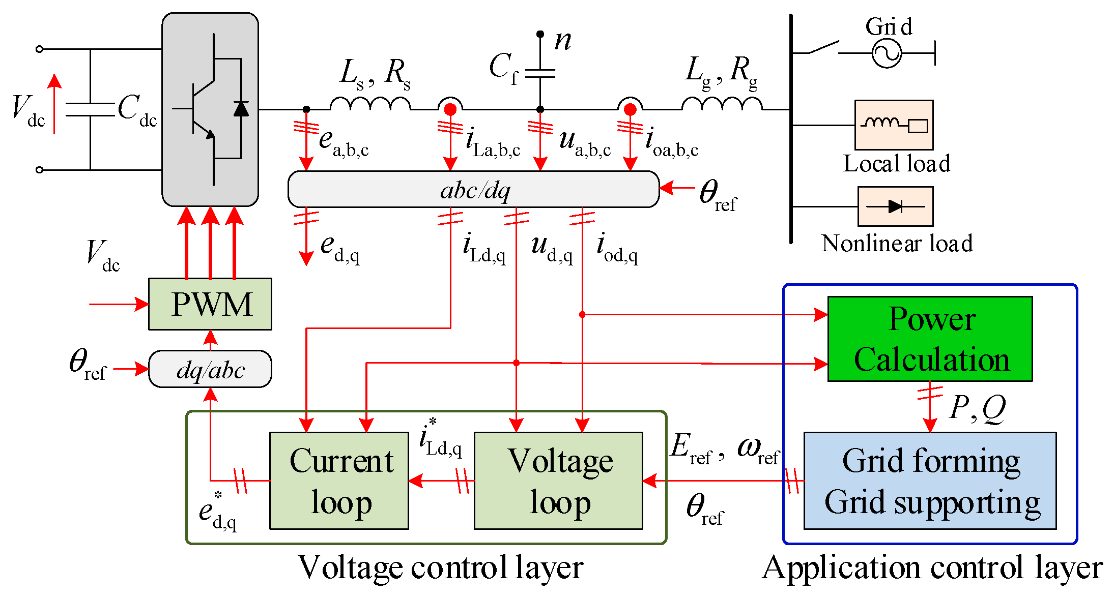
A typical topology and control structure of the three-phase voltage-controlled MG inverter is shown in Figure 1. The application control layer realizes the droop control or VSG control, generates the amplitude reference, , and frequency reference, , according to different control targets. The voltage control layer then tracks the instantaneous reference voltage rapidly in the SRF and adjusts the output impedance. The PWM algorithm is used to generate the driving signals of the switching devices.
Fast and stable voltage control is the guarantee of reliable operation of the inverter. As the lower control layer, the inner voltage control should achieve a zero-dynamic voltage control [6]. This paper focuses on the inner voltage control; the application control layer is not discussed.
The direct current (DC) side is usually equipped with an energy storage system (ESS) or bus capacitors, and the voltage stabilization control algorithm is adopted to maintain a constant bus voltage, ; is the voltage of the inverter side; and and are the output voltage and current of the inverter. The LC filter includes the filter inductor, , equivalent series resistance, , and the filter capacitor, ; and represent the current of the filter inductor and capacitor. and are line impedances; is the output of the voltage loop and is the output of the current loop; local loads are paralleled on the point of common coupling (PCC).
2.1. Inverter Modelling in SRF
According to Figure 1, the mathematical model of the three-phase inverter with an LC filter is given in the SRF [3]:
where , , , and are the d-axis and q-axis components of and ; , , , and are the d-axis and q-axis components of and ; and ( Hz in this study) is the fundamental frequency of the output voltage.
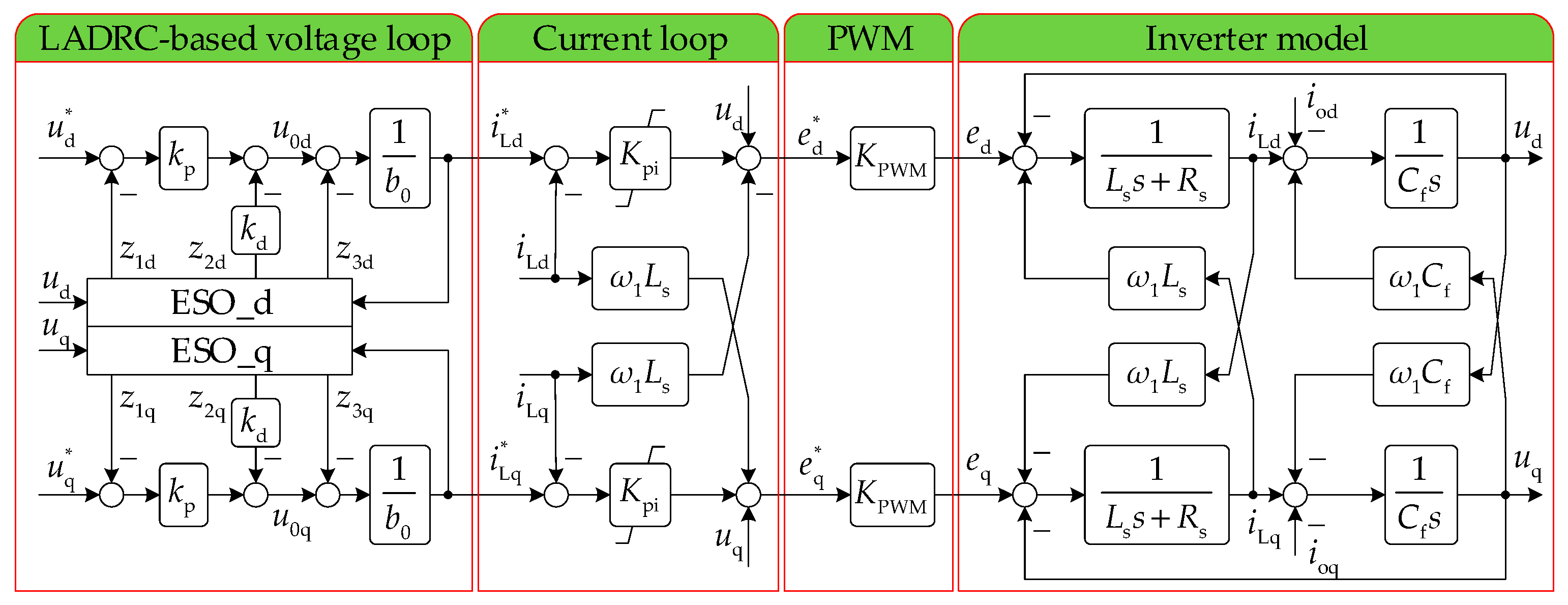
The inverter model in the SRF is obtained by Laplace transformation of (1), as shown in Figure 2, where s represents the Laplace transform operator and the superscript * represents the reference value of the variable.
2.2. Structure of LADRC-Based Voltage Loop
The voltage controller scheme based on LADRC is shown in Figure 2. A dual-loop control (DLC) structure is used. The inner current loop is utilized to control the inductor current with the PI-based regulator, and the outer voltage loop is used to control the capacitor voltage with the LADRC-based regulator.
To simplify the analysis, the delay caused by sampling and calculation is ignored. The PWM inverter gain , so . To improve the response speed, the current loop uses a proportional controller with a gain of . The current loop regulator is:
where and are the output of the current loop and are compared to the PWM carrier to generate the switching signal; and are the output of the voltage loop and the reference of the current loop.
The closed loop transfer function of the current loop is:
Combined with Equations (1) and (3), the voltage loop is designed based on LADRC, as shown in Figure 2. Ignoring , the controlled object of the outer voltage loop is obtained:
where, and are the defined disturbance of dq axis respectively, .
From Figure 2 and Equation (5), the controlled object of the outer voltage loop is a second-order system, so two second-order LADRC controllers with third-order LESO need to be designed in the dq axis. The coupling between the dq axis can be regarded as a part of the total disturbance. Decoupling can be performed through feedforward compensation, so the controllers of the dq axis can be designed as separate channels with the same structure as LADRC. Simply take the d axis as an example.
An LADRC comprises LESO and LSEF. Wherein, the total disturbance is expanded into a new state. Then LESO is adopted to estimate the total disturbance and other state information. Finally, LSEF integrates all the state information obtained from LESO and reconstructs the system state equation.
From Equation (5), the state variables and output are defined as:
Then, the following state-space equation can be derived:
where is the system input and is the system control gain (CG). Considering the uncertainty of , its estimated value is used, which is generally ; is often called the compensation factor (CF); denotes the total disturbance, which includes external disturbance, internal dynamics, and the estimation error between CG and CF [29].
By extending as a separate state, , of the system, and assuming that is differentiable with , then the system model can be represented in state space:
The third-order LESO of the system can be designed as:
where , , and are the state variables of LESO. , , and are the observer gain.
By choosing the appropriate observer gain, the state variables of the system can be tracked quickly by the LESO in Equation (9), which is , , .
Through taking the Laplace transformation of Equation (9), we have:
To achieve good disturbance rejection, the estimation variable is added into the control input; LSEF can be designed as:
where and are gains of LSEF, is the intermediate variable, and is the reference input.
If the LESO is reliable and the estimation error of CG is negligible, then , , , and . According to Equations (7) and (11), the closed-loop transfer function of the system can be deduced:
Combining Equations (10) and (12), the characteristic Equation of LESO and the closed-loop transfer function are:
According to the parameterization technique proposed [18], the eigenvalues of the LESO and the closed-loop transfer function can be located at and . Then, is the bandwidth of the LESO and is the bandwidth of the controller in LADRC. The tuning details are given by:
With the above configuration, the dynamic performance of the system is dependent on only two parameters, which are the controller bandwidth, , and the observer bandwidth, . With appropriate bandwidth parameters, the system can track the reference input without overshoot.
The design process of the outer voltage loop controller based on LADRC in the d-axis is completed, including Equations (9), (11), and (14). The simplified structure of the original LADRC-based controller is shown in Figure 3. The controller in the q axis can be designed regarding the d axis and will not be described in detail.
2.3. Influence of Observer Bandwidth and Compensation Factor
After designing the LADRC-based voltage loop completely, the next step is tuning the parameters to satisfy the requirements of stability and dynamic performance in the system; is chosen by the requirements of dynamic performance and is generally not an adjustable parameter.
Affected by discrete period and measurement noise, there exists a trade-off between observation accuracy and noise rejection ability when choosing . Furthermore, CG in the actual system is hard to obtain. It can be seen from Equation (7) that the selection of and the perturbation of some parameters, such as inductance and capacitance, will also lead to deviation from the theoretical value, resulting in . Therefore, it is essential and important to study the influence of CF and on system stability, anti-disturbance, and noise rejection ability.
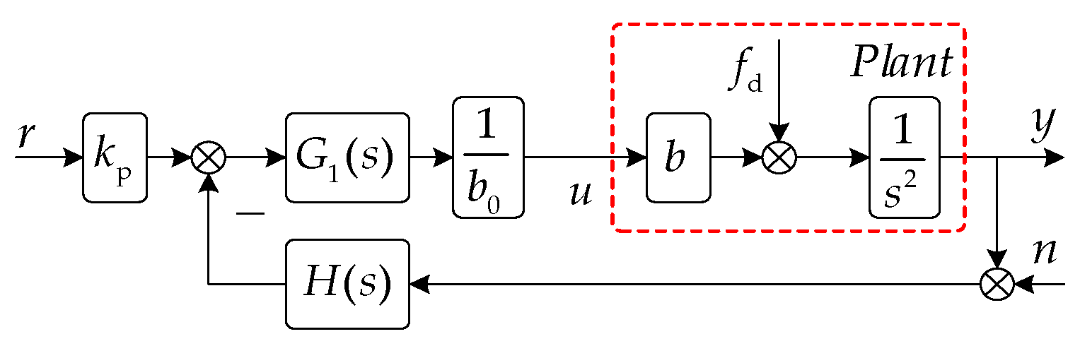
According to Equations (10) and (14), and considering the system model (7) and the measurement noise , the control structure of LADRC can be simplified, as shown in Figure 4. The control input of the system is:
where , , and are the Laplace transformation of r, y, and n, and , .
Let , which represents the ratio of CF to CG. The output of the system is:
where .
From Equation (16), the system output consists of a tracking term, a disturbance term, and a measurement noise term; , , and are related to the system’s stability, dynamic performance, anti-disturbance, and noise rejection ability. In order to study the observer bandwidth constraints and the influence of CF, the amplitude-frequency characteristics (called Bode diagram) and root locus diagram are adopted respectively in this subsection.
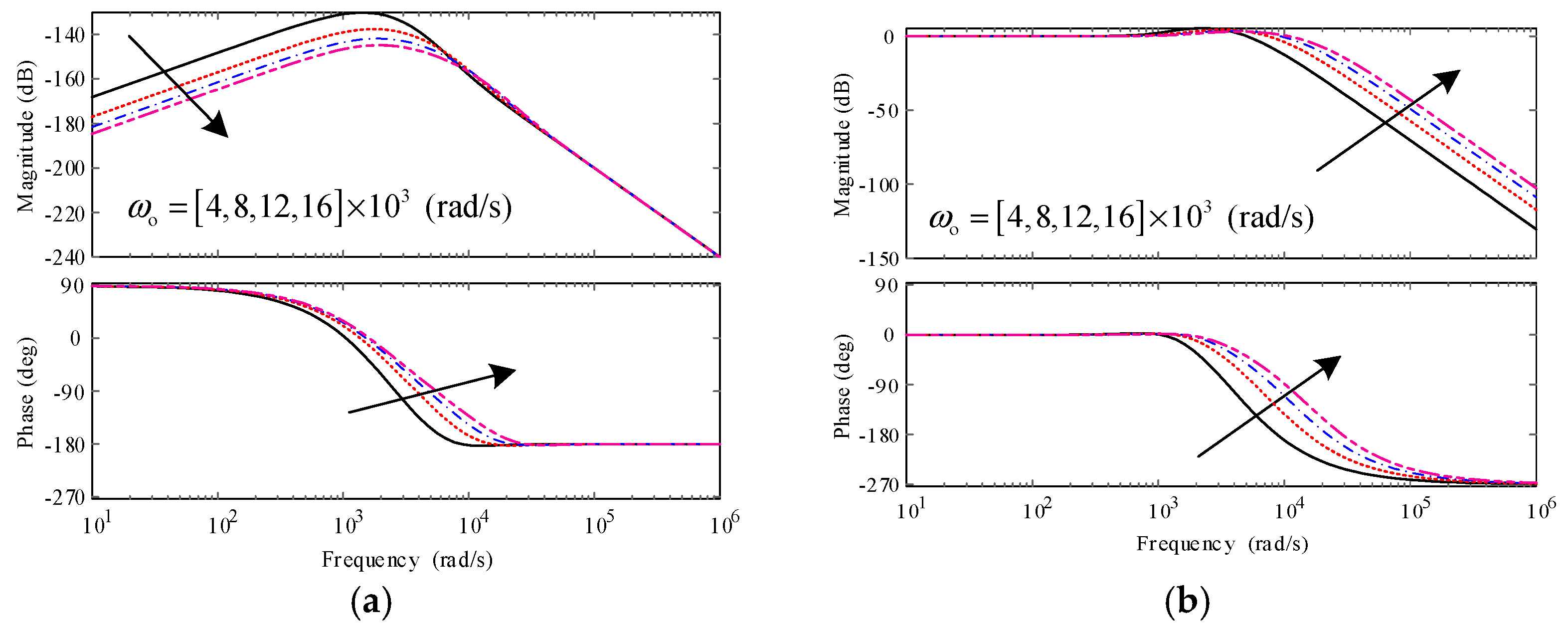
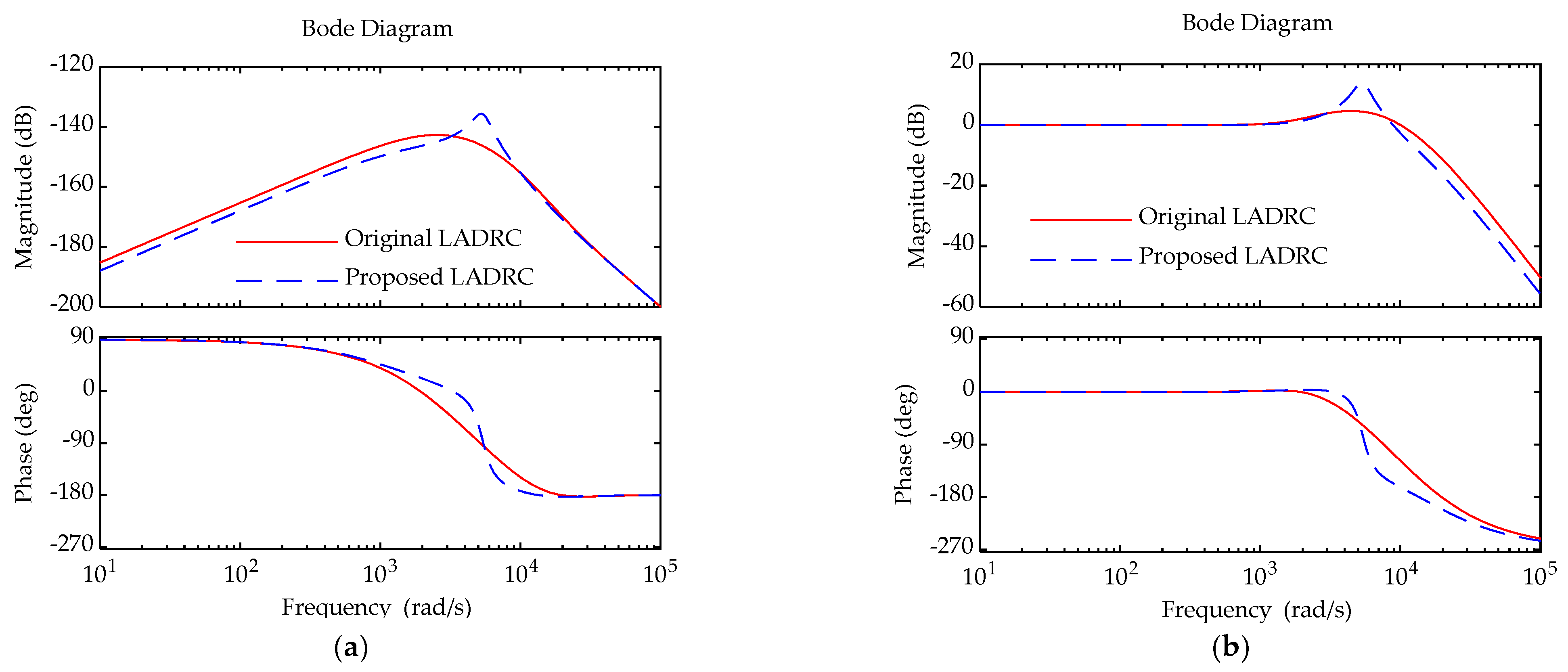
The Bode diagram of the transfer function with different has been studied in [19,20,21,22,25,26], so they are not mentioned in this paper. The Bode diagrams of the transfer function and are given in Figure 5, where and . It can be seen that increasing can reduce the low-frequency gain of , which can enhance the system’s anti-disturbance ability. On the contrary, the high-frequency gain of is increased, so the system becomes more sensitive to the measurement noise. Thus, there is a trade-off between anti-disturbance and noise rejection ability when choosing .
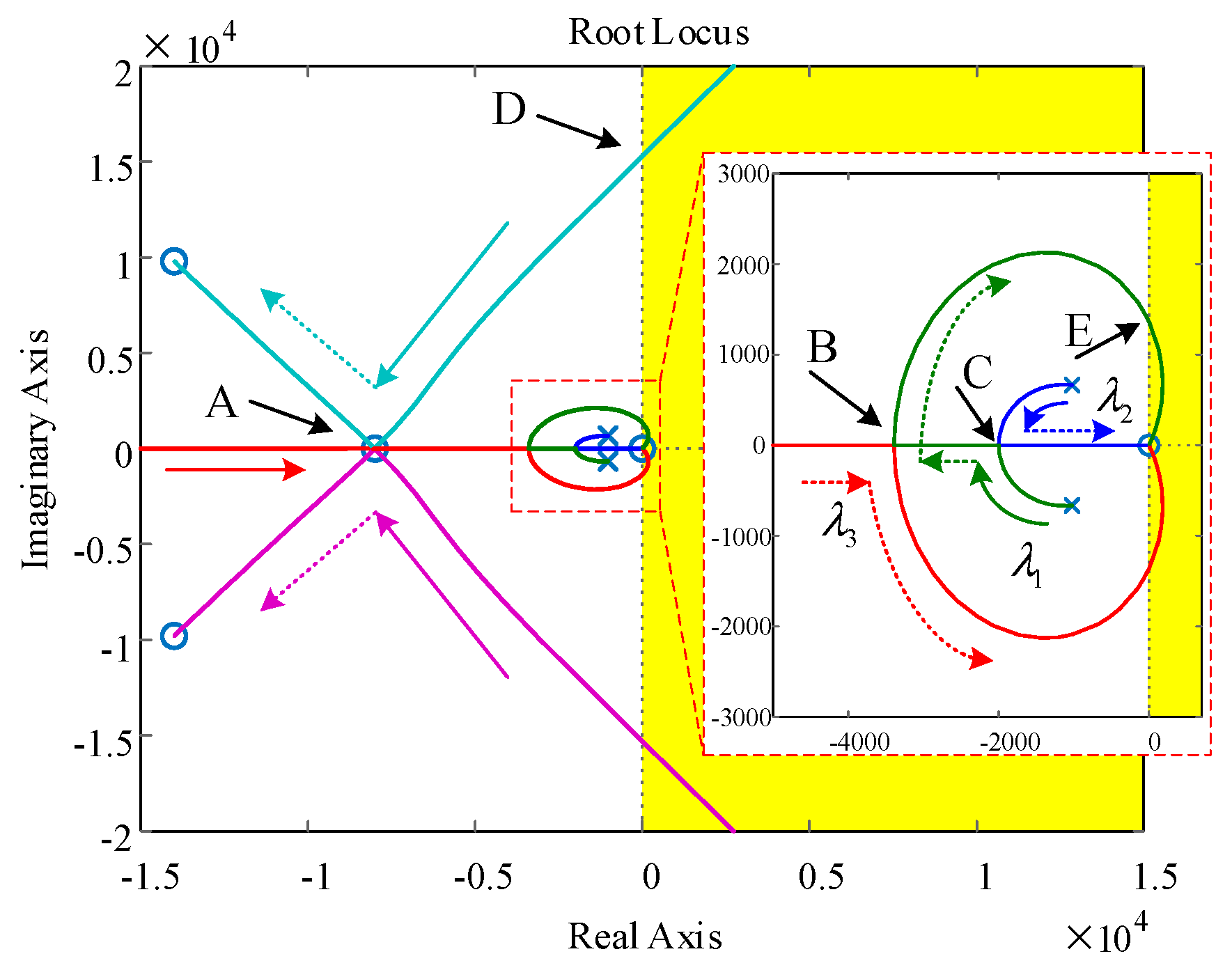
In Equation (16), does not affect the closed-loop zero position; only affecting the pole position, so a root locus diagram is adopted to analyze the dynamic performance and robustness of . To obtain better observation accuracy, is generally chosen between 2 to 10 [30]. Let rad/s; the root locus with different is shown in Figure 6. The yellow area represents the unstable regions caused by the right-half-plane poles. The solid arrow represents the pole change when increases from 0 to 1, while the dashed arrow represents the situation when increases from 1 to infinity.
In Figure 6, it can be seen that:
- When , the poles are located at points A and C on the real axis, corresponding to and , and the system has no overshoot and a short settling time;
- When changes from 0 to infinite, if is smaller than 1.02 (point D), or greater than 5.24 (point E), the system will be unstable. The range of that makes the system stable is listed in Table 1. As increases, the stable range of is expanded.
- When increases from 0 to 1, poles enter the stable regions and approach point A and C. Poles , , and are closer to the imaginary axis, so are marked as dominant poles. With increasing, and gradually move away from the imaginary axis and approach the real axis, so the response time and overshoot decreases and the damping increases.
- When increases from 1 to 1.02 (point B), , , and are on the real axis and there is no overshoot in response. When they continue to increase, poles approach the imaginary axis, and the damping becomes smaller. This shows that the response becomes slower, and there is both overshoot and damped oscillation, then poles cross the negative half axis, and the system becomes unstable.
3. Known Disturbance Compensation Scheme
The observation accuracy of LESO directly affects the performance of LADRC. To enhance the anti-disturbance ability of the inverter system, a simple way is to increase the bandwidth of the LESO. Consequently, a better ability will be obtained to deal with the voltage fluctuation under the load switch. However, is limited by the discrete period and measurement noise.
3.1. Design of Proposed Scheme
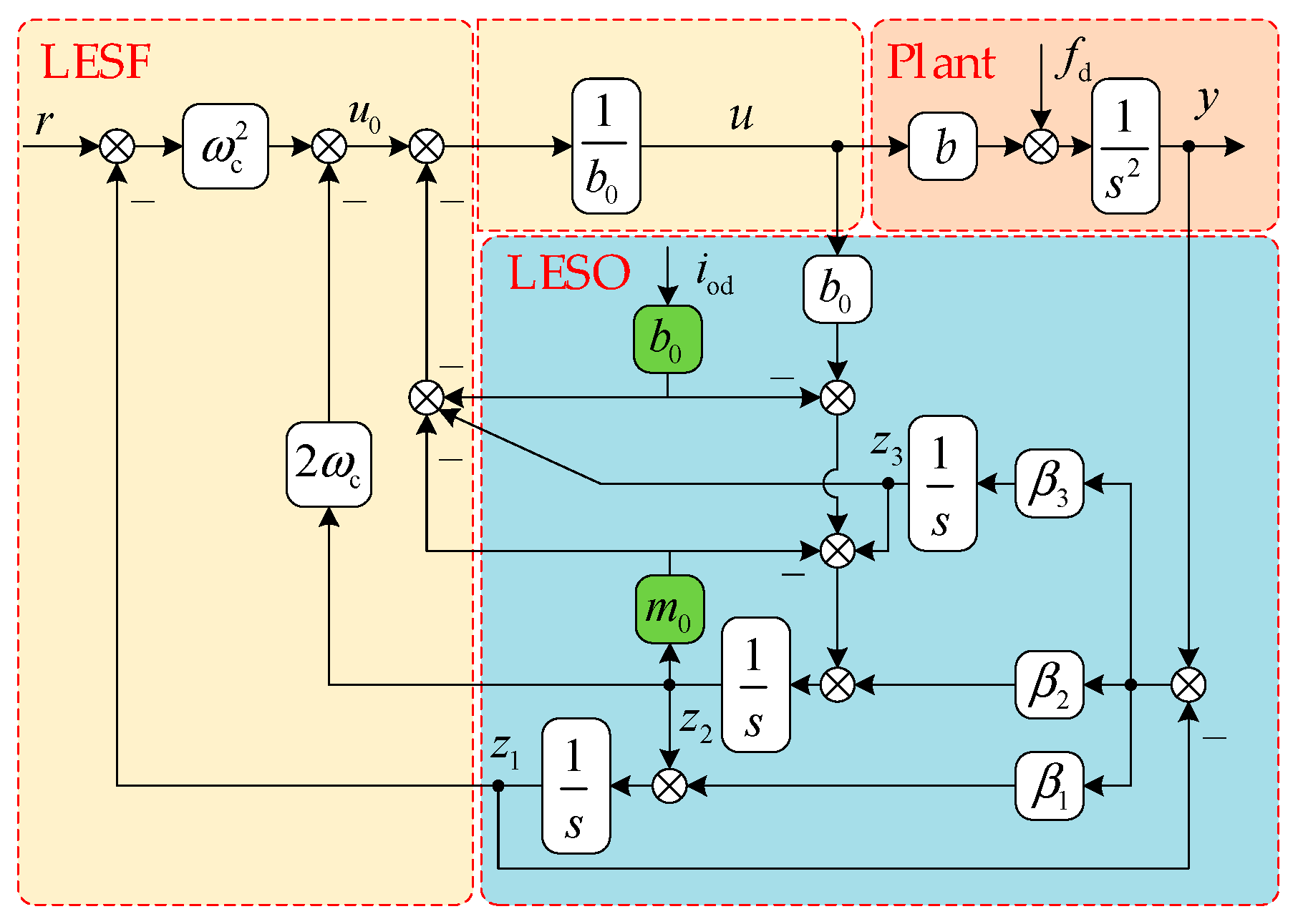
An improved LADRC scheme based on the known disturbance compensation is proposed in this paper, as shown in Figure 7. The known disturbance consists of model information and load current.
According to Equation (7), the d-axis component of the plant can be rewritten as:
where and is the model information; represents load current disturbance. The remaining disturbances, , are part of , and .
The system model (8) can be rewritten as
where is the differential of .
Different from the original LADRC, the system state matrix is changed because of introducing model information, and the LESO is designed as:
where . Note that is the estimated value of instead of .
Then, taking the Laplace transformation of Equation (19), we have:
So the closed-loop poles of the observer (20) are at the roots of:
After parameterization, the poles are allocated at the same position, . Then LESO gains are, respectively:
The load current can be compensated by feedforward, then the LSEF is changed to:
3.2. Analysis of the Proposed Scheme
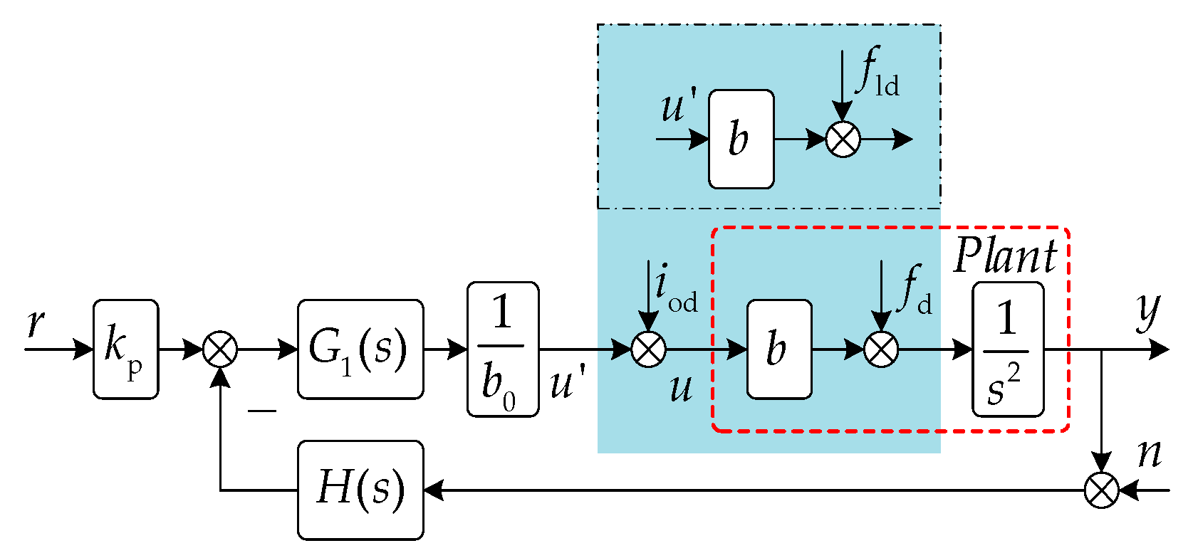
According to Equations (20) and (23), the control structure of LADRC can be simplified, as shown in Figure 8, in which . The control input of the system is:
where , .
So the output of the system is:
where .
As seen in Figure 9a, the proposed LADRC scheme has a smaller low-frequency gain than the original LADRC scheme, so the proposed LADRC has better anti-disturbance performance and a stronger ability to restraint input disturbance than the original LADRC in the low-frequency band. Similarly, the proposed LADRC has better noise rejection performance because of the lower high-frequency gain in Figure 9b.
3.3. Stability Analysis
Let , in which , , and represent the estimation error of LESO. According to Equations (18) and (19), the estimation error is:
where .
Theorem 1.
Assuming that is bounded, namely , such that there exists a LESO that can make the estimation error boundary and .
Proof.
Choosing to make:
Then there exists a reversible real matrix T that makes:
So:
And , is used in Equation (29), so:
where is a constant.
Solving Equation (26), the:
Considering the compatibility of and in the complex field, then:
This shows that the estimation error of LESO can converge to a small boundary without an accurate mathematical model. As the observer bandwidth increases, the boundary decreases, and the estimation accuracy improves.
From Figure 8 and Equations (22) and (24), the closed-loop transfer function of the system is:
where .
The Lienard–Chipard criterion can be applied to judge whether the system is stable or not. The necessary and sufficient condition for stability is that the coefficients of the characteristic equation and each odd (or even) order Hurwitz determinant are greater than zero separately. Therefore, the stability condition of the system can be simplified as:
In Equations (22) and (33), are related to , and are related to . Thus, the stability of the system can be guaranteed by selecting an appropriate and according to the restriction conditions in Equation (34). □
3.4. Load Current Estimator
By introducing load current information, the influence of load current disturbance can be decreased. Therefore, the voltage drops during the load switch can be reduced. Consequently, the anti-disturbance ability of inverters can be significantly improved. However, the load current sensors undoubtedly increase the cost. As an alternate method, a load current estimation method is proposed that does not require current sensors.
In practice, the derivation of capacitor voltage with a low-pass filter (LPF) is used to estimate the load current, but it needs the differential signals of the voltage. The observer, such as a disturbance observer [31] or sliding mode observer [32], is also an effective method to obtain the load current, but it needs to be designed separately, increasing the system complexity. In this paper, the LESO observation state is used to simplify the design of load current observation.
According to Equations (1) and (9), observation values of load current can be obtained by:
where, can be obtained from current sensors; , , , and are the output of the LESO in Equation (20).
From the analysis in reference [33], the state matrix of LESO in Equation (20) can be Hurwitz when the appropriate observer bandwidth is taken. Therefore, the estimation error can converge to zero in a finite time, . That is , , , and . Hence, the load current can be estimated by (35).
In addition, the estimated load current is introduced to LESO and subtracted in LESF. After simplification, the estimated load current can be regarded as perturbations outside the forward channel, as shown in Figure 8. Then the estimation error of the load current will be reflected in the total disturbance and does not affect the stability of the system.
4. Simulation and Experimental Verification
In the proposed scheme, the model information belongs to internal disturbance and cannot be changed independently, while the load disturbance belongs to external disturbance and can be controlled by increasing or decreasing the load. Thus the reference step simulation and experiment of capacitor voltage under no-load condition has been carried out to validate the feasibility of the model information compensation scheme. The voltage tracking capability is compared with the original LADRC scheme, in which the load current is 0, so only the model information compensation scheme works. During load switching, the load current dominates the total disturbance and the proportion of the model information disturbance is small. Thus the load switch simulation and experiment have been carried out to validate the feasibility of the load current compensation scheme, and the voltage drop is used to evaluate the ability to suppress the load disturbance.
4.1. Discretization of LESO
In simulation and experiment, the proposed scheme was discretized with the bilinear transformation method (BTM), and the discrete period equals the sampling period, .
In the system model (18), let:
So the LESO with the proposed scheme (19) can be rewritten as:
For the convenience of digital implementation, only the LESO is discretized using BTM, and we have:
where, , , , and is the observer gain matrix.
For tuning simply, the poles of the desired discrete LESO characteristic equation are placed at , where . Then the desired characteristic polynomial is
So the observer gain L can be derived:
Then the discrete form of LESO can be obtained by substituting Formula (40) into Formula (38). The discrete implementation of LSEF (23) is:
4.2. Simulation Results
The simulation model was first established through MATLAB/Simulink. Table 2 lists the key parameters of the inverter and controller in simulation. To verify the feasibility of the proposed scheme, the original LADRC (marked as OL) scheme, the only model information compensation (marked as MC) scheme, the only load current compensation (marked as LC) scheme, the proposed (MC and LC, marked as PS) scheme, and the estimated load current scheme with model information (marked as ES) were studied.
The simulation process is as follows: 0–0.1 s; the reference voltage linearly increases from 0 to 60 V and remains 60 V until 0.1 s, then steps to 120 V at 0.185 s and remains 120 V until the end of the simulation. The resistive loads (20 per phase) are added at 0.305 s. The deviation of 5 ms is to ensure that the reference change and load switch are at the approximately maximum of the A-phase voltage.
The simulation results of the OL, MC, LC, and PS schemes are shown in Figure 10. Under the no-load condition, the load current is 0, so the LC scheme did not work. Therefore, the OL and LC curves are approximately coincident, the same as theMC and PS curves. In Figure 10a, four schemes can track the reference voltage well, but the OL and LC schemes have obvious voltage overshoot (132.04 V) when the reference voltage steps at 0.185 s. The MC scheme can effectively improve the dynamic performance at the reference tracking, and the voltage overshoot is reduced to 123.18 V.
During load switching, load current disturbance is dominant in the total disturbance, so the LC scheme has better anti-disturbance performance than the MC scheme, as shown in Figure 10b. The comparison of the voltage drop and settling time between different schemes is listed in Table 3. The MC scheme has little effect on the load switch. On the other hand, the LC scheme can effectively reduce voltage drops and settling time when the load switches. Therefore, the proposed scheme can well combine the advantages of the two schemes.
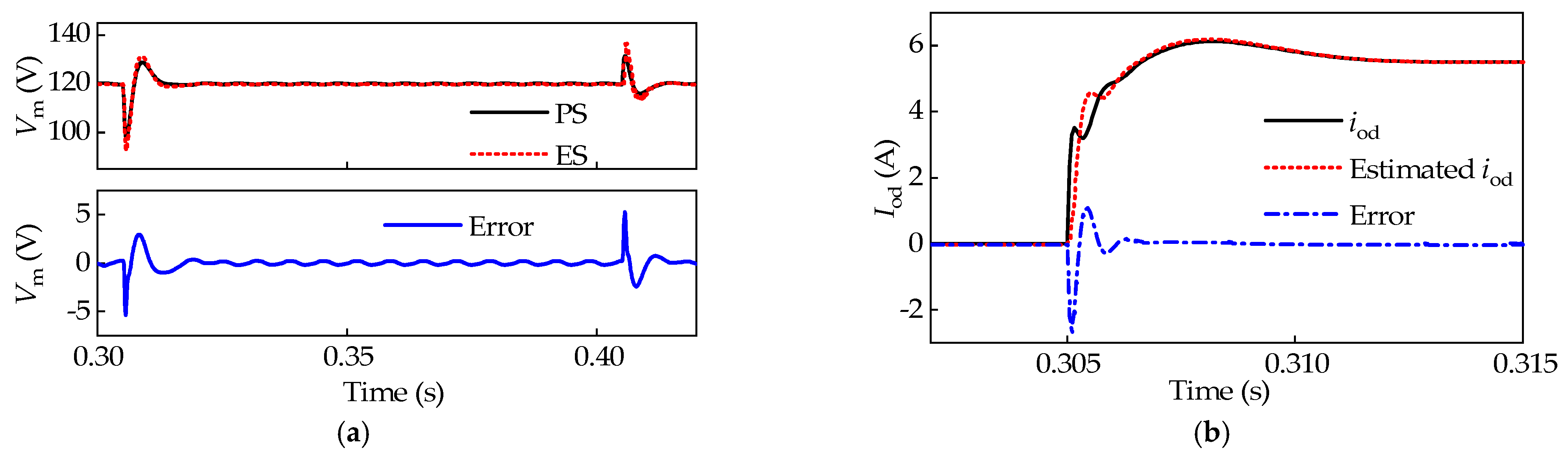
The simulation results of the PS and ES schemes are shown in Figure 11. Both schemes can reduce voltage drop when loads switch. The voltage error between the ES and PS schemes is less than 6 V, and is less than 0.4 V at the steady-state. The d-axis load current can be estimated in real time and stabilized in 2 ms, as shown in Figure 11b. The maximum estimation error is lower than 2.6 A when the loadis switched, and is less than 0.02 A at the steady-state.
THD (%) values under different schemes in the simulation are listed in Table 4. Under no-load conditions, the MC, PS, and ES schemes can reduce the THD to 0.23% and 0.35%, while LC has little effects because there is no load current. Under full load conditions, although the voltage drop decreases because of the load current feedforward, the voltage THD in the steady-state increases because delays caused by sampling and filtering result in incomplete compensation of the load current. The THD values of the ES scheme are close to the PS scheme because of the small estimation error, as shown in Figure 11.
4.3. Experiment Results
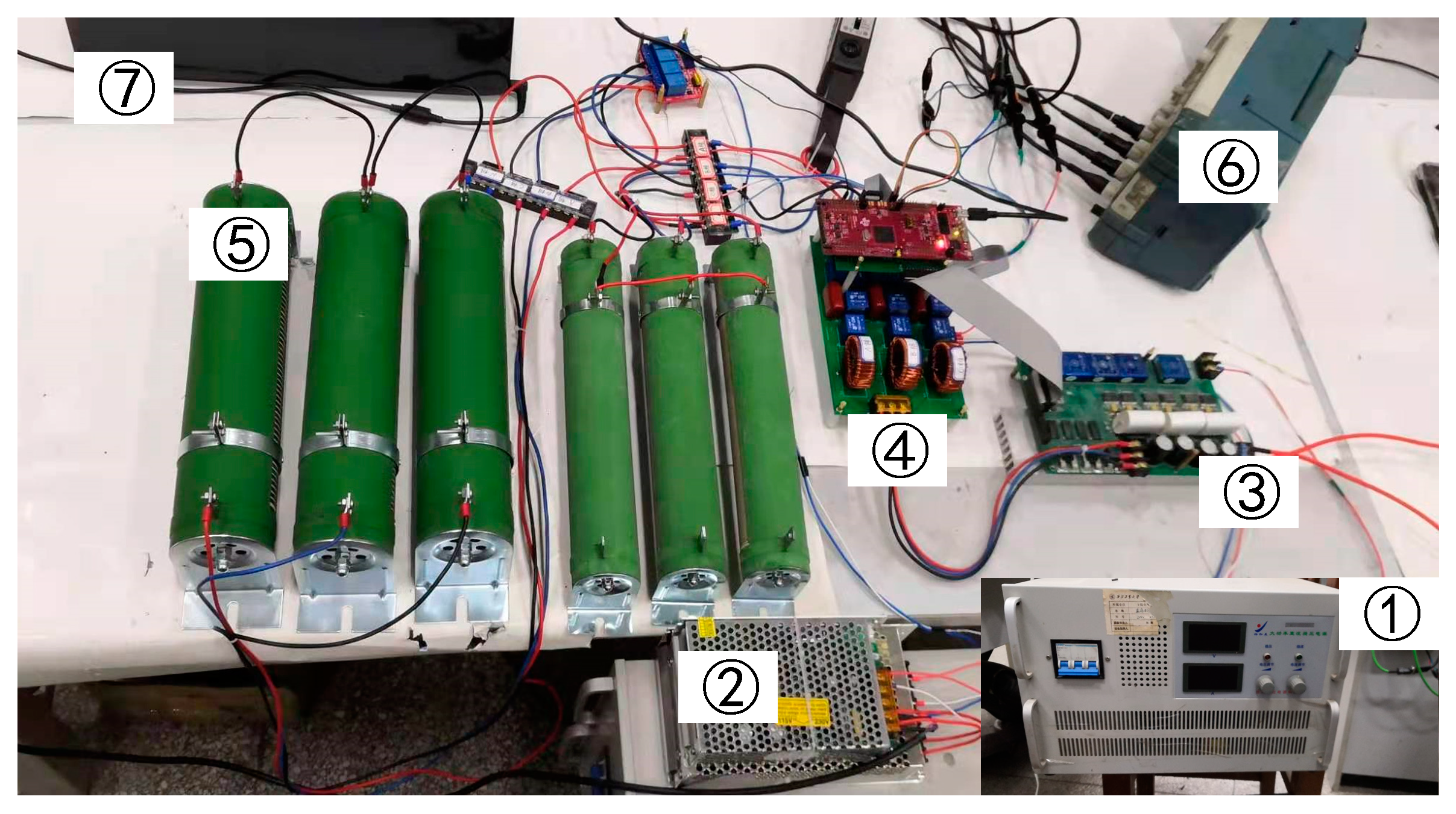
The experimental platform is shown in Figure 12. It is comprised of an LC-filtered three-phase inverter, the DC power supply, and linear load. The DC bus is replaced by a 300 V/20 A DC power supply. A TI LaunchPad 28379D board was used to implement the control algorithm. The switching frequency of the IGBT module is set to 10 kHz, and the dead time is 2.6 μs. The sampling period is 100 μs. TBC10SYW and TBV10/25A are applied to measure the three-phase current and voltage. A Tektronix A622 current probe is used to measure the A-phase load current. In the actual system, the measurement noise is worse, so rad/s and rad/s, less than the values in the simulation. Other parameters are listed in Table 2.
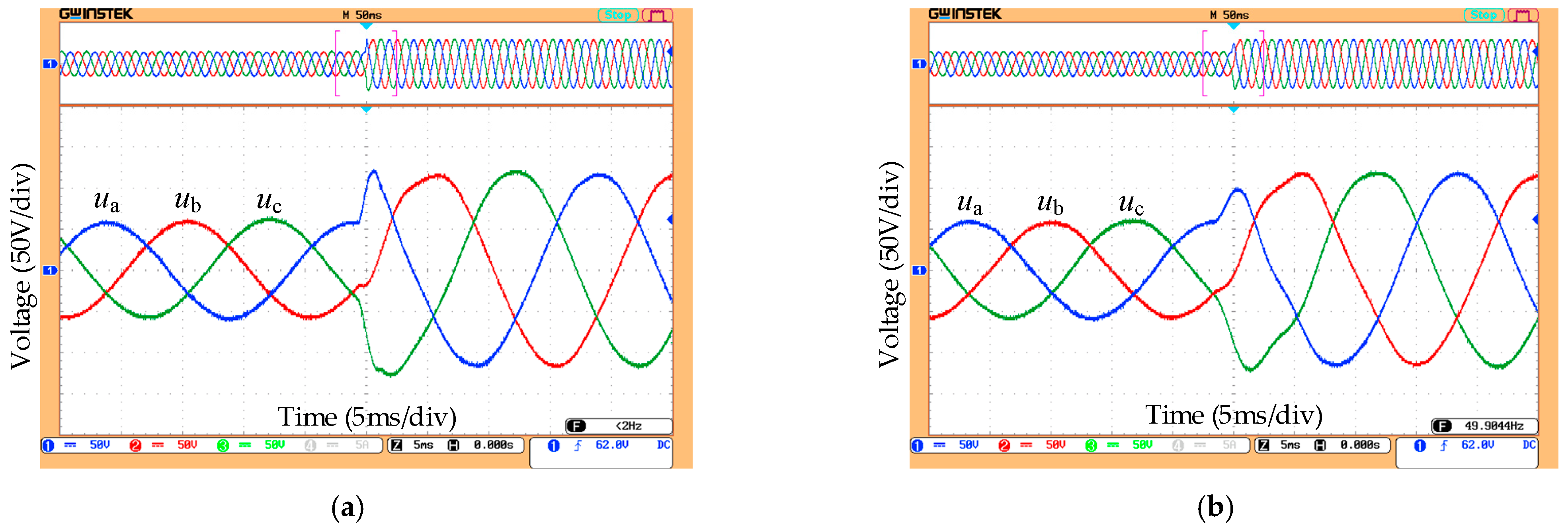
Figure 13 shows the experimental results of the capacitor voltage with different schemes under no load, in which the amplitude of the reference voltage rises to 120 V from 60 V. The load current is 0, so only MC works. LC and ES schemes are not presented here. The system can remain stable before and after the reference steps with both schemes.
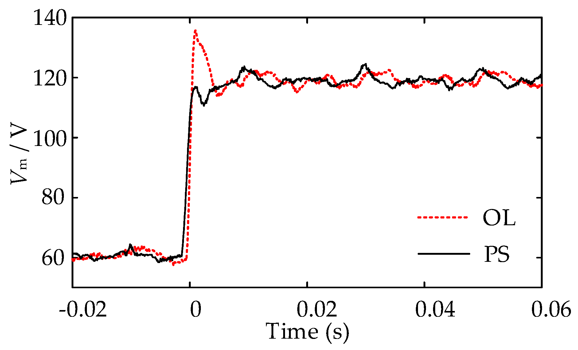
As shown in Figure 14, the voltage of the OL and PS schemes track well the reference voltage, 60 V and 120 V, and can recover within 4 ms, but the overshoot of the OL scheme is up to 134 V, which is greater than the PS scheme. The amplitude of the capacitor voltage is calculated from , where represents the i-phase voltage sampled by the oscilloscope.
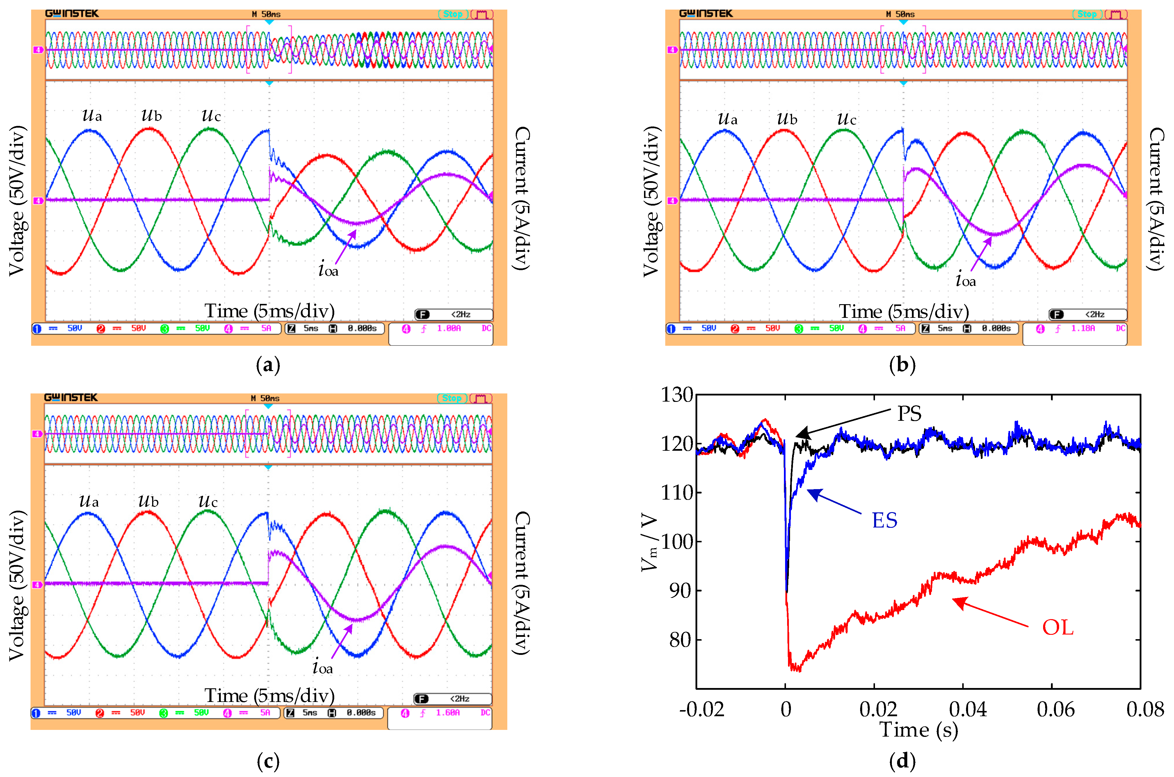
In the case of load switching (adding 20 Ω resistor per phase), the load current changes dramatically, so the instantaneous total disturbance is too large. In order to avoid the system divergence caused by control saturation, a saturation module is added after and . The experimental results of the capacitor voltage and the A-phase load current are shown in Figure 15. Due to a lack of known disturbance compensation, the observation accuracy is limited. After adding the load, the voltage cannot be recovered within one period with the OL scheme, and the voltage drops to 74.4 V when the load switches. With the PS scheme, the voltage drops to 89.6 V and can recover within 4 ms with no overshoot. Similar to the PS scheme, the voltage drops to 90.2 V and recovers within 10 ms with the ES scheme, which is slower than the PS scheme.
In the experiment, THD (%) values under different schemes are calculated by the FFT Analysis Tool in Matlab/Simulink, and they are listed in Table 5. Under no-load conditions, the PS scheme can reduce the THD to 0.85% and 0.89% with model information compensation. Similar to the simulation results, the output voltage quality was worse with the PS scheme, and the THD was 1.86%, higher than the OL scheme, 1.67%. Additionally, the voltage THD under full load conditions was 1.67%, higher than the no-load conditions (1.25% and 1.38%); this may be caused by control saturation because of the slower response, as shown in Figure 15a. Under full-load conditions, the THD value with the ES scheme is 1.96%, which is 0.1% different from the PS scheme, and the difference under no-load conditions is 0.05%. So the estimation error of the load current affects the voltage quality.
5. Conclusions
A LADRC-based voltage control strategy with known disturbance compensation is proposed for voltage-controlled inverters based on a dual-loop structure. The compromise between the anti-disturbance and noise rejection ability is studied. The constraint of the observer bandwidth affects the anti-disturbance ability, so the model information and load current are regarded as the known disturbance and introduced into the LESO to further enhance the anti-disturbance ability. The comparison between original and proposed LADRC schemes is then provided by the frequency domain response. Furthermore, the stability of the proposed LESO and LADRC is analyzed. For saving the current sensors, an estimated load current feedforward scheme is also mentioned. The theoretical analysis, simulation, and experimental results show that: (1) The model information can effectively improve the system’s dynamic performance. The overshoot and settling time of the voltage dynamics is reduced, the same as THD values. (2) The load current compensation can reduce the voltage drop under the load switch and enhance the anti-disturbance ability. However, the voltage THD is increased due to the delays introduced by sampling and filtering. Moreover, as an alternate method, the estimated load current feedforward scheme does not need load current sensors and has a similar dynamic performance and ability of voltage drop suppression as the proposed scheme.
Power quality issues, such as harmonics and unbalanced voltage, have not been discussed in this paper. In future work, the LADRC strategy will be designed for positive-sequence, negative-sequence, and selected harmonic voltage controller to improve power quality. Furthermore, the compensation factor will be designed adaptively according to the voltage drop or estimation error to further enhance the anti-disturbance ability of the system.
Author Contributions
Conceptualization, Y.L., R.Q.; methodology, Y.L., M.D.; software, X.Z., Y.Z.; validation, Y.L., M.D.; formal analysis, Y.L., Y.Z.; investigation, X.Z.; resources, R.Q.; data curation, Y.Z.; writing—original draft preparation, Y.L., M.D.; writing—review and editing, X.Z., Y.Z.; visualization, M.D., Y.Z.; supervision, R.Q.; project administration, R.Q.; funding acquisition, R.Q. All authors have read and agreed to the published version of the manuscript.
Funding
This research was funded by the National Natural Science Foundation of China, grant number 51777170, and the National Natural Science Foundation of Shanxi Province, grant number 2020JM-151.
Conflicts of Interest
The authors declare no conflict of interest.
Abbreviations
| Acronym | Definition |
| LADRC | Linear active disturbance rejection control |
| VCI | Voltage-controlled inverter |
| LESO | Linear extended state observer |
| DERs | Distributed energy resources |
| RES | Renewable energy sources |
| MG | Microgrid |
| PI | Proportional-integral |
| PWM | Pulse width modulation |
| THD | Total harmonic distortion |
| RC | Repetitive control |
| LSEF | Linear state error feedback |
| SRF | Synchronous reference frame |
| PCC | Point of common coupling |
| CG | Control gain |
| CF | Compensation factor |
| LPF | Low-pass filter |
| BTM | Bilinear transformation method |
References
- Hosseinzadeh, N.; Aziz, A.; Mahmud, A.; Gargoom, A.; Rabbani, M. Voltage Stability of Power Systems with Renewable-Energy Inverter-Based Generators: A Review. Electronics 2021, 10, 115. [Google Scholar] [CrossRef]
- Arbab-Zavar, B.; Palacios-Garcia, E.; Vasquez, J.; Guerrero, J. Smart Inverters for Microgrid Applications: A Review. Energies 2019, 12, 840. [Google Scholar] [CrossRef] [Green Version]
- Hossain, M.A.; Pota, H.R.; Issa, W.; Hossain, M.J. Overview of AC microgrid controls with inverter-interfaced generations. Energies 2017, 10, 1300. [Google Scholar] [CrossRef]
- Rocabert, J.; Luna, A.; Blaabjerg, F.; Rodríguez, P. Control of Power Converters in AC Microgrids. IEEE Trans. Power Electron. 2012, 27, 4734–4749. [Google Scholar] [CrossRef]
- Bouzid, A.M.; Guerrero, J.M.; Cheriti, A.; Bouhamida, M.; Sicard, P.; Benghanem, M. A survey on control of electric power distributed generation systems for microgrid applications. Renew. Sustain. Energy Rev. 2015, 44, 751–766. [Google Scholar] [CrossRef] [Green Version]
- Quan, X.; Dou, X.; Wu, Z.; Hu, M.; Song, H.; Huang, A.Q. A Novel Dominant Dynamic Elimination Control for Voltage-Controlled Inverter. IEEE Trans. Ind. Electron. 2018, 65, 6800–6812. [Google Scholar] [CrossRef]
- Dou, C.; Zhang, Z.; Yue, D.; Song, M. Improved droop control based on virtual impedance and virtual power source in low-voltage microgrid. IET Gener. Transm. Distrib. 2017, 11, 1046–1054. [Google Scholar] [CrossRef]
- Buso, S.; Caldognetto, T.; Brandao, D.I. Dead-beat current controller for voltage source converters with improved large-signal response. IEEE Trans. Ind. Appl. 2015, 52, 1588–1596. [Google Scholar] [CrossRef]
- Lim, K.; Choi, J. Seamless Grid Synchronization of a Proportional+Resonant Control-Based Voltage Controller Considering Non-Linear Loads under Islanded Mode. Energies 2017, 10, 1514. [Google Scholar] [CrossRef] [Green Version]
- Komurcugil, H.; Altin, N.; Ozdemir, S.; Sefa, I. Lyapunov-Function and Proportional-Resonant-Based Control Strategy for Single-Phase Grid-Connected VSI with LCL Filter. IEEE Trans. Ind. Electron. 2016, 63, 2838–2849. [Google Scholar] [CrossRef]
- Zhang, M.; Huang, L.; Yao, W.; Lu, Z. Circulating Harmonic Current Elimination of a CPS-PWM-Based Modular Multilevel Converter With a Plug-In Repetitive Controller. IEEE Trans. Power Electron. 2014, 29, 2083–2097. [Google Scholar] [CrossRef]
- Marati, N.; Prasad, D. A Modified Feedback Scheme Suitable for Repetitive Control of Inverter With Nonlinear Load. IEEE Trans. Power Electron. 2018, 33, 2588–2600. [Google Scholar] [CrossRef]
- Yaramasu, V.; Rivera, M.; Narimani, M.; Wu, B.; Rodriguez, J. Model Predictive Approach for a Simple and Effective Load Voltage Control of Four-Leg Inverter With an Output LC Filter. IEEE Trans. Ind. Electron. 2014, 61, 5259–5270. [Google Scholar] [CrossRef]
- Mahdian Dehkordi, N.; Sadati, N.; Hamzeh, M. A backstepping high-order sliding mode voltage control strategy for an islanded microgrid with harmonic/interharmonic loads. Control Eng. Pract. 2017, 58, 150–160. [Google Scholar] [CrossRef]
- Komurcugil, H. Improved passivity-based control method and its robustness analysis for single-phase uninterruptible power supply inverters. IET Power Electron. 2015, 8, 1558–1570. [Google Scholar] [CrossRef]
- Rymarski, Z.; Bernacki, K.; Dyga, Ł.; Davari, P. Davari Passivity-Based Control Design Methodology for UPS Systems. Energies 2019, 12, 4301. [Google Scholar] [CrossRef] [Green Version]
- Han, J. From PID to Active Disturbance Rejection Control. IEEE Trans. Ind. Electron. 2009, 56, 900–906. [Google Scholar] [CrossRef]
- Gao, Z. Active disturbance rejection control: A paradigm shift in feedback control system design. In Proceedings of the 2006 American Control Conference, Minneapolis, MN, USA, 14–16 June 2006; p. 7. [Google Scholar] [CrossRef]
- Benrabah, A.; Xu, D.; Gao, Z. Active Disturbance Rejection Control of LCL-Filtered Grid-Connected Inverter Using Padé Approximation. IEEE Trans. Ind. Appl. 2018, 54, 6179–6189. [Google Scholar] [CrossRef]
- Zhang, H.; Xian, J.; Shi, J.; Wu, S.; Ma, Z. High Performance Decoupling Current Control by Linear Extended State Observer for Three-Phase Grid-Connected Inverter With an LCL Filter. IEEE Access 2020, 8, 13119–13127. [Google Scholar] [CrossRef]
- Cao, Y.; Zhao, Q.; Ye, Y.; Xiong, Y. ADRC-Based Current Control for Grid-Tied Inverters: Design, Analysis, and Verification. IEEE Trans. Ind. Electron. 2020, 67, 8428–8437. [Google Scholar] [CrossRef]
- Zhang, Y.; Zhu, J.; Dong, X.; Zhao, P.; Ge, P.; Zhang, X. A Control Strategy for Smooth Power Tracking of a Grid-Connected Virtual Synchronous Generator Based on Linear Active Disturbance Rejection Control. Energies 2019, 12, 3024. [Google Scholar] [CrossRef] [Green Version]
- Yu, Y.; Hu, X. Active Disturbance Rejection Control Strategy for Grid-Connected Photovoltaic Inverter Based on Virtual Synchronous Generator. IEEE Access 2019, 7, 17328–17336. [Google Scholar] [CrossRef]
- Li, S.; Li, Y.; Chen, X.; Jiang, W.; Li, X.; Li, T. Control strategies of grid-connection and operation based on active disturbance rejection control for virtual synchronous generator. Int. J. Electr. Power Energy Syst. 2020, 123, 106144. [Google Scholar] [CrossRef]
- Ma, W.; Guan, Y.; Zhang, B. Active Disturbance Rejection Control Based Control Strategy for Virtual Synchronous Generators. IEEE Trans. Energy Convers. 2020, 35, 1747–1761. [Google Scholar] [CrossRef]
- Zeng, J.; Huang, Z.; Huang, Y.; Qiu, G.; Li, Z.; Yang, L.; Yu, T.; Yang, B. Modified linear active disturbance rejection control for microgrid inverters: Design, analysis, and hardware implementation. Int. Trans. Electr. Energy Syst. 2019, 29. [Google Scholar] [CrossRef]
- Li, H.; Li, S.; Lu, J.; Qu, Y.; Guo, C. A Novel Strategy Based on Linear Active Disturbance Rejection Control for Harmonic Detection and Compensation in Low Voltage AC Microgrid. Energies 2019, 12, 3982. [Google Scholar] [CrossRef] [Green Version]
- Wu, G.; Sun, L.; Lee, K.Y. Disturbance rejection control of a fuel cell power plant in a grid-connected system. Control Eng. Pract. 2017, 60, 183–192. [Google Scholar] [CrossRef]
- Zhou, R.; Tan, W. A generalized active disturbance rejection control approach for linear systems. In Proceedings of the IEEE 10th Conference on Industrial Electronics and Applications (ICIEA), Auckland, New Zealand, 15–17 June 2015; pp. 248–255. [Google Scholar] [CrossRef]
- Fu, C.; Tan, W. Tuning of linear ADRC with known plant information. ISA Trans. 2016, 65, 384–393. [Google Scholar] [CrossRef] [PubMed]
- Wu, Y.; Ye, Y. Internal Model-Based Disturbance Observer With Application to CVCF PWM Inverter. IEEE Trans. Ind. Electron. 2018, 65, 5743–5753. [Google Scholar] [CrossRef]
- Guo, L.; Li, Y.; Jin, N.; Dou, Z.; Wu, J. Sliding mode observer-based AC voltage sensorless model predictive control for grid-connected inverters. IET Power Electron. 2020, 13, 2077–2085. [Google Scholar] [CrossRef]
- Zheng, Q.; Dong, L.; Lee, D.H.; Gao, Z. Active Disturbance Rejection Control for MEMS Gyroscopes. IEEE Trans. Control Syst. Technol. 2009, 17, 1432–1438. [Google Scholar] [CrossRef]
Figure 1.
Topology and control structure of the three-phase voltage-controlled MG inverter.

Figure 2.
LADRC-based voltage control scheme.

Figure 3.
Structure of original LADRC-based voltage control scheme.

Figure 4.
Simplified structure of the second-order LADRC.

Figure 5.
Bode diagrams with different : (a) Disturbance term ; (b) Noise term .

Figure 6.
Root locus diagram of with different .

Figure 7.
Proposed LADRC scheme based on known disturbance compensation.

Figure 8.
Simplified structure of the proposed LADRC scheme.

Figure 9.
Bode diagrams with different schemes: (a) Disturbance term ; (b) Noise term .

Figure 10.
Simulation results: (a) Reference steps at 0.185 s; (b) Adding load at 0.305 s.

Figure 11.
Simulation comparisons between PS and ES schemes under load switching. (a) Voltage amplitude; (b) D-axis load current and estimated value after adding load.
Figure 11.
Simulation comparisons between PS and ES schemes under load switching. (a) Voltage amplitude; (b) D-axis load current and estimated value after adding load.

Figure 12.
Experimental platform. ① DC power supply; ② Control power source; ③ Inverter bridge; ④ LC filters, sensors, and DSP; ⑤ Loads; ⑥ Oscilloscope; ⑦ Computer.
Figure 12.
Experimental platform. ① DC power supply; ② Control power source; ③ Inverter bridge; ④ LC filters, sensors, and DSP; ⑤ Loads; ⑥ Oscilloscope; ⑦ Computer.

Figure 13.
Experimental results under the reference voltage change: (a) Original LADRC scheme; (b) Proposed scheme.
Figure 13.
Experimental results under the reference voltage change: (a) Original LADRC scheme; (b) Proposed scheme.

Figure 14.
Amplitude of capacitor voltage under the reference voltage step.

Figure 15.
Experimental results under load switching. (a) Original LADRC scheme; (b) Proposed scheme; (c) Estimated load current scheme; (d) Amplitude of different schemes.
Figure 15.
Experimental results under load switching. (a) Original LADRC scheme; (b) Proposed scheme; (c) Estimated load current scheme; (d) Amplitude of different schemes.


Table 1.
Stable range of with different and .
| 2000 | 4000 | 2 | 0.247~4.11 |
| 2000 | 8000 | 4 | 0.208~5.24 |
| 2000 | 12,000 | 6 | 0.185~6.51 |
Table 2.
Key parameters of inverter and controller in simulation.
| Symbol | Quantity | Value |
|---|---|---|
| DC bus voltage | 300 V | |
| Filter inductor | 3.0 mH | |
| Inductor resistor | 0.16 Ω | |
| Filter capacitor | 14 μF | |
| Switching frequency | 10 kHz | |
| Sampling period | 100 μs | |
| Voltage amplitude/frequency | 120 V/50 Hz | |
| The gain in the current loop | 18.8 | |
| Controller bandwidth in LADRC | 3142 rad/s | |
| Observer bandwidth in LADRC | 10,472 rad/s |
Table 3.
Simulation results of the voltage drop and settling time between different schemes.
| Schemes | Voltage Drop (V) | Voltage Maximum (V) | Settling Time (ms) |
|---|---|---|---|
| OL | 48.47 | 19 | |
| MC | 51.51 | 21 | |
| LC | 99.62 | 130.62 | 8 |
| PS | 97.86 | 128.79 | 7 |
Table 4.
THD (%) values under different schemes in the simulation.
| Schemes | No Load (60 V) | No Load (120 V) | Full Load (120 V) |
|---|---|---|---|
| OL | 0.26 | 0.39 | 0.21 |
| MC | 0.23 | 0.34 | 0.18 |
| LC | 0.26 | 0.39 | 0.42 |
| PS | 0.23 | 0.35 | 0.34 |
| ES | 0.24 | 0.35 | 0.36 |
Table 5.
THD (%) values under different schemes in the experiment.
| Schemes | No Load (60 V) | No Load (120 V) | Full Load (120 V) |
|---|---|---|---|
| OL | 1.25 | 1.38 | 1.67 |
| PS | 0.85 | 0.89 | 1.86 |
| ES | 0.88 | 0.94 | 1.96 |
Publisher’s Note: MDPI stays neutral with regard to jurisdictional claims in published maps and institutional affiliations. |
© 2021 by the authors. Licensee MDPI, Basel, Switzerland. This article is an open access article distributed under the terms and conditions of the Creative Commons Attribution (CC BY) license (https://creativecommons.org/licenses/by/4.0/).
Share and Cite
MDPI and ACS Style
Li, Y.; Qi, R.; Dai, M.; Zhang, X.; Zhao, Y. Linear Active Disturbance Rejection Control Strategy with Known Disturbance Compensation for Voltage-Controlled Inverter. Electronics 2021, 10, 1137. https://doi.org/10.3390/electronics10101137
AMA Style
Li Y, Qi R, Dai M, Zhang X, Zhao Y. Linear Active Disturbance Rejection Control Strategy with Known Disturbance Compensation for Voltage-Controlled Inverter. Electronics. 2021; 10(10):1137. https://doi.org/10.3390/electronics10101137
Chicago/Turabian StyleLi, Yang, Rong Qi, Mingguang Dai, Xi Zhang, and Yiyun Zhao. 2021. "Linear Active Disturbance Rejection Control Strategy with Known Disturbance Compensation for Voltage-Controlled Inverter" Electronics 10, no. 10: 1137. https://doi.org/10.3390/electronics10101137
Note that from the first issue of 2016, this journal uses article numbers instead of page numbers. See further details here.