Article

Antenna on Chip (AoC) Design Using Metasurface and SIW Technologies for THz Wireless Applications

by
Ayman A. Althuwayb
1,*,
Mohammad Alibakhshikenari
2,*,
Bal S. Virdee
3,
Harry Benetatos
3,
Francisco Falcone
4,5 and
Ernesto Limiti
2
1
Department of Electrical Engineering, College of Engineering, Jouf University, Sakaka, Aljouf 72388, Saudi Arabia
2
Electronic Engineering Department, University of Rome “Tor Vergata”, Via del Politecnico 1, 00133 Rome, Italy
3
Center for Communications Technology & Mathematics, School of Computing & Digital Media, London Metropolitan University, London N7 8DB, UK
4
Electric, Electronic and Communication Engineering Department, Public University of Navarre, 31006 Pamplona, Spain
5
Institute of Smart Cities, Public University of Navarre, 31006 Pamplona, Spain
*
Authors to whom correspondence should be addressed.
Electronics 2021, 10(9), 1120; https://doi.org/10.3390/electronics10091120
Submission received: 19 March 2021 / Revised: 23 April 2021 / Accepted: 6 May 2021 / Published: 10 May 2021
(This article belongs to the Special Issue Advances in System-on-Chip Design)

Abstract

:
This paper presents the design of a high-performance 0.45–0.50 THz antenna on chip (AoC) for fabrication on a 100-micron GaAs substrate. The antenna is based on metasurface and substrate-integrated waveguide (SIW) technologies. It is constituted from seven stacked layers consisting of copper patch–silicon oxide–feedline–silicon oxide–aluminium–GaAs–copper ground. The top layer consists of a 2 × 4 array of rectangular metallic patches with a row of subwavelength circular slots to transform the array into a metasurface. This essentially enlarges the effective aperture area of the antenna. The antenna is excited using a coplanar waveguide feedline that is sandwiched between the two silicon oxide layers below the patch layer. The proposed antenna structure reduces substrate loss and surface waves. The AoC has dimensions of 0.8 × 0.8 × 0.13 mm3. The results show that the proposed structure greatly enhances the antenna’s gain and radiation efficiency, and this is achieved without compromising its physical size. The antenna exhibits an average gain and efficiency of 6.5 dBi and 65%, respectively, which makes it a promising candidate for emerging terahertz applications.

1. Introduction

Smart wireless devices have grown in popularity at an exponential rate. This has caused an explosion of data traffic in the limited prescribed bandwidth resources [1]. It is estimated that the data rate in the next decade is going to be in the order of Tbps [2,3]. Although it has been shown that THz communication can easily provide a Gbps data rate, we are at a nascent stage of development for data rates in the Tbps [4,5]. THz waves benefit from being sandwiched between the millimeter and light waves in the electromagnetic spectrum. Compared with millimeter waves, THz waves have a wider usable frequency band and focused beam directivity that makes them highly unsusceptible to interference issues. Compared with light waves, THz waves have a stronger penetration power [6].
Antennas have a direct bearing on the performance of wireless systems in terms of operating bandwidth, radiation gain, and efficiency. These parameters have an impact on the system’s data transmission rate, imaging resolution, and range. Compared with millimeter waves, the design of THz antennas is highly challenging as THz antennas operate at much higher frequencies and their size is significantly smaller. Moreover, the packaging of THz antennas is limited by materials and process technologies. Additionally, free-space path loss is an inevitable characteristic of all wireless communication. However, THz waves are greatly absorbed by the atmosphere. Hence, increasing the gain of the THz antenna is an important requirement to compensate for the free-space path loss. Moreover, THz antennas suffer from relatively high loss, which makes them currently impractical for on-chip fabrication.
An antenna is the first element in a wireless receiver and the last element in a transmitter. To guarantee optimum power transfer between the antenna and the RF-integrated circuitry, it is necessary to include an impedance matching network at the junction of the antenna and the RF circuitry. Typically, antennas are matched to a 50 Ohm impedance system, which normally requires converting the complex impedance of the system to 50 Ohm [7]. This is achieved by employing conjugate matching, in which the imaginary section of two impedances has an identical magnitude but reverse signs. Additionally, bond wires are used to connect the THz antenna to the integrated circuit. As bond wires are not characterized well at THz, the matching is often suboptimal [6].
On-chip realizations of antennas overcome the abovementioned limitations as impedances of integrated circuit elements do not need to be matched with 50 Ohm [8,9,10]. Co-design of circuits and antennas guarantee that complex impedances are conjugately matched with no need for a matching circuit, thus saving several additional elements, area, expense, and numerous design attempts. Furthermore, the antenna on chip (AoC) omits any doubt with bond-wires as metal interlinks are used to interface the integrated circuit to the antenna feed point [11].
Antennas for on-chip applications need to be planar as they need to be fabricated using the same integrated circuit processing. A low-resistivity substrate (10–20 Ω cm) is a common choice for the fabrication of CMOS circuits, which is necessity to overcome the latch-up issue. This type of substrate, however, greatly limits the efficiency of planar antennas resulting from high ohmic and dielectric loss in the underlying silicon substrate. A dipole antenna fabricated on a 10 Ωcm silicon substrate typically has a limited efficiency of 10% [12,13].
Proposed in this paper is a technique to overcome the limitations on bandwidth, gain, and efficiency of THz antennas fabricated on-chip. This is achieved by employing two different technologies, namely a substrate-integrated waveguide (SIW) and a 2D metamaterial, which is commonly referred to as a metasurface [14]. The proposed technique reduces the loss due to the substrate and suppresses the adverse effects of surface waves. The results confirm this has notable improvement in the radiation characteristics of AoC.

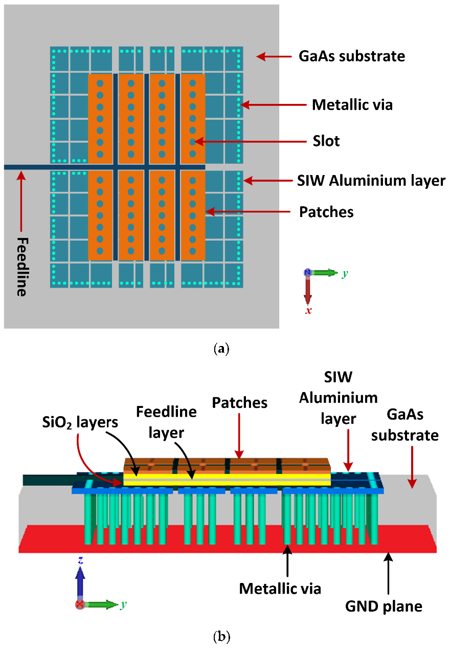
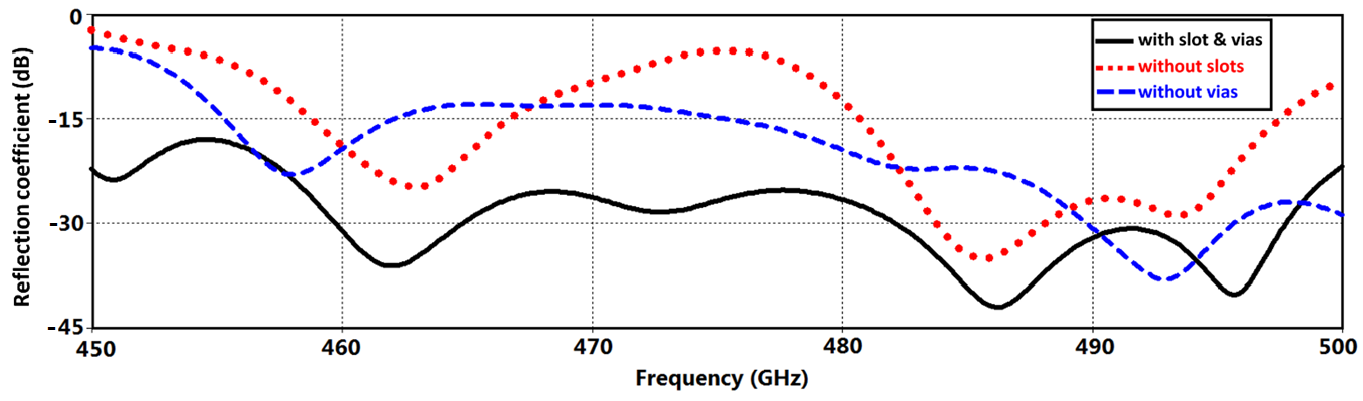
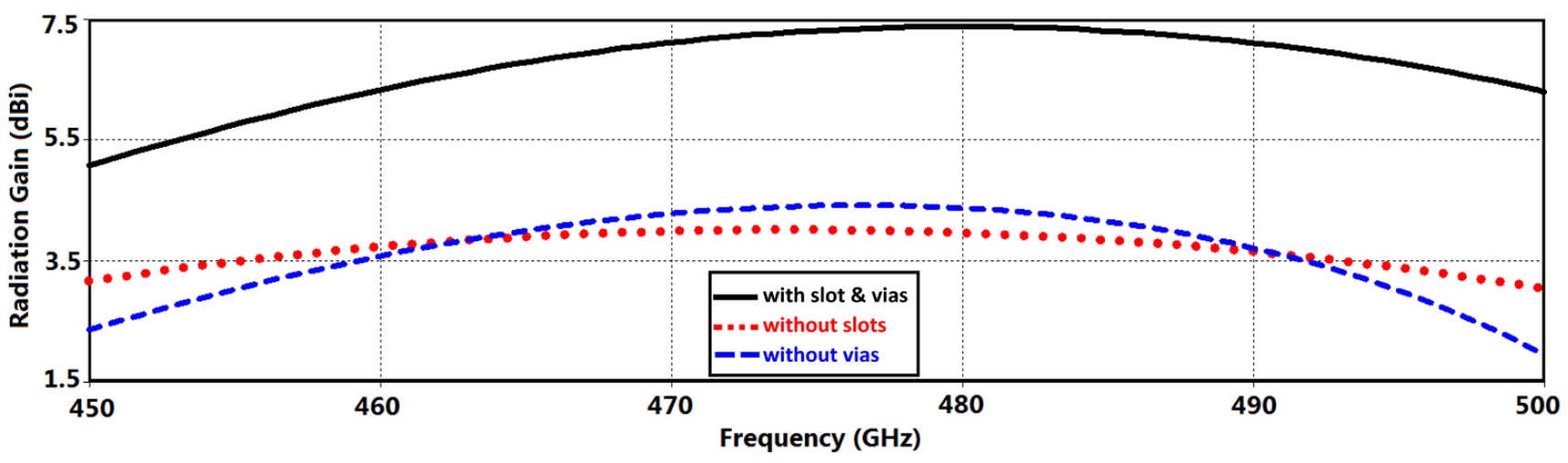
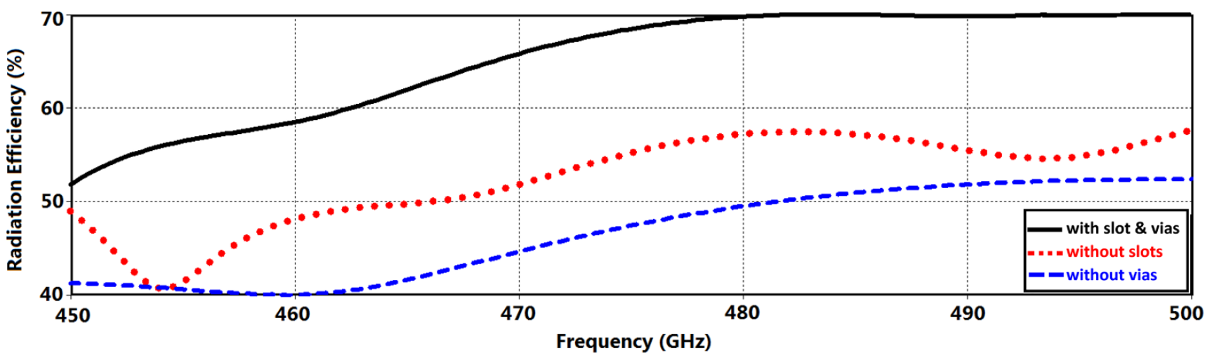
2. Antenna on Chip Design

The proposed AoC is constituted from several stacked layers comprising Cu–SiO2–Cu–SiO2–Al–GaAs–Cu as shown in Figure 1. The top layer consists of a 2 × 4 array of rectangular copper patches. Etched on the patches is a row of subwavelength circular slots. The antenna is excited using proximity coupling at the patch edge, which is analogous to a gap coupling patch. This is achieved with a microstrip coplanar waveguide feedline, which is created by having both sides next to the feedline grounded. The feedline is sandwiched between the two silicon oxide layers, below which is a layer with aluminium patches that are separated from each other by a narrow gap. This layer acts like a partially reflective surface. The outer periphery of the aluminium patches is studded with an arrangement of densely lined metallic posts or vias connecting it to the ground-plane through the GaAs substrate to create a SIW electromagnetic resonant cavity. Incident electromagnetic waves that penetrate through the gaps in the aluminium layer are reflected at the ground-plane. The thickness of the GaAs substrate is such that the phase shift of the ground-plane reflected waves is in phase with the waves reflected at the surface of the copper patches. With this arrangement, the aluminium surface acts like an artificial magnetic conductor (AMC) that fully reflects incident waves with a near zero degrees reflection phase [15]. This configuration results in significantly enhanced directivity. The circular slots across the rectangular patches act like miniature resonators that radiate energy at the THz band. The antenna was implemented on a GaAs substrate of 100-micron thickness, a dielectric constant of 12.94, and a loss-tangent of 0.006.
The proposed SIW structure reduces substrate loss, radiation leakage, and adverse effects of surface wave propagation. This is achieved by carefully choosing the diameter and spacing of the metallic vias [16]. The subwavelength circular slots transform the array into a metasurface that has an effect of amplifying the effective aperture area of the antenna, the consequence of which is an enhancement in the radiation gain and efficiency of the antenna. In addition, the slots also improve the impedance match and bandwidth of the antenna.
The optimized structural parameters of the proposed AoC are given in Table 1. Optimization was done using CST Microwave Studio, which is a 3D full-wave electromagnetic simulation tool. The optimization involved parameterizing the antenna structure to achieve the target goal of |S11| ≤ −10 dB across 450–500 GHz. The optimizer used in CST Microwave Studio was the Covariance Matrix Adaptation Evolutionary Strategy (CMA-ES). This optimizer was used because it has a relatively fast convergence, and it uses the history of the previous iterations to improve the performance of the algorithm while avoiding local optimums. The AoC has a form factor of 0.8 × 0.8 × 0.13 mm3. The effect of the circular slots and metallic vias on the performance parameters of the AoC are shown in Figure 2, Figure 3 and Figure 4. It is evident that the metasurface and SIW significantly improve the antenna’s impedance bandwidth to better than S11 ≤ −15 dB, and the radiation gain and efficiency to over 0.45–0.5 THz. The average impedance match over 0.45–0.5 THz is approximately 30 dB, which an improvement of 15 dB without the slots and vias. The antenna has a fractional bandwidth of 10.52%. By incorporating the slots in the patches, the average radiation gain of the antenna increases to 6.5 dBi. This is an improvement of 2.7 dBi without the slots. The corresponding radiation efficiency increases to approximately 65%, which is an improvement of 12% without the slots. The average gain with the inclusion of the metallic vias is 6.5 dBi, which is an improvement of 4.4 dBi without the vias. The average efficiency with the metallic vias increases to about 65%, which is an improvement of 19% without the vias.
The E-plane and H-plane radiation patterns of the proposed AoC at 0.45 THz are shown in Figure 5. Clearly, the radiation patterns exhibit relatively high directivity in both planes. The half-power beam width in the xy-plane is 26° and that in the xz-plane is 17°. In addition, the side-lobe and back-lobe levels are all below −17.5 dBi in the xz-plane and below −22 dBi in the xy-plane.

3. Comparison with State-of-the-Art AoC

Table 2 compares the salient features of the proposed on-chip antenna with AoC reported in the literature. The maximum gain of the proposed antenna of 7.4 dBi is lower than [17,18] but it is comparable to references [11,19,20]. Additionally, it has a maximum efficiency of 70%, which is lower than [17,19,20] but it is comparable to [11]. However, compared with the cited work in Table 2 the proposed antenna operates over a much higher frequency (between 450 and 500 GHz). Moreover, other than the antenna in [21] that operates over a much lower frequency range (50–70 GHz), the proposed antenna is much less thick with respect to the operating wavelength than other on-chip antennas reported to date. This is attributed to combining metasurface and SIW technologies in the implementation of the on-chip antenna. The thinner antenna structure is important to prevent the generation of surface or substrate modes that can adversely affect the antenna’s performance, especially at THz frequencies [22].

4. Conclusions

The innovative design of an antenna is described for on-chip applications for terahertz applications. It is shown that by combining metasurface and SIW technologies in the antenna design, its impedance bandwidth, radiation gain, and efficiency performance are substantially enhanced. This is achieved without increasing the aperture area of the antenna. The antenna is constructed on a GaAs substrate and is composed of a 2 × 4 array of rectangular patches with a row of circular slots etched on it. It is excited through a microstrip coplanar waveguide feedline. Compared to AoC reported in the literature, the proposed antenna has a larger frequency bandwidth and operates at a much higher frequency with comparable gain and radiation efficiency.

Author Contributions

Conceptualization, A.A.A., M.A., B.S.V., H.B., F.F., and E.L.; methodology, M.A., B.S.V., and E.L.; software, A.A.A., M.A., and B.S.V.; validation, A.A.A., M.A., B.S.V., H.B., F.F., and E.L.; formal analysis, M.A., B.S.V., and F.F.; investigation, M.A., B.S.V., F.F., and E.L.; resources, A.A.A., M.A., B.S.V., H.B., F.F., and E.L.; data curation, A.A.A., M.A., B.S.V., H.B., F.F., and E.L.; writing—original draft preparation, A.A.A. and M.A.; writing—review and editing, A.A.A., M.A., B.S.V., H.B., F.F., and E.L.; visualization, M.A., B.S.V., F.F., and E.L.; supervision, M.A., F.F., and E.L.; project administration, M.A., F.F., and E.L.; funding acquisition, M.A., F.F., and E.L. All authors have read and agreed to the published version of the manuscript.

Funding

This work is partially supported by RTI2018-095499-B-C31, Funded by Ministerio de Ciencia, Innovación y Universidades, Gobierno de España (MCIU/AEI/FEDER, UE).

Institutional Review Board Statement

Not applicable.

Informed Consent Statement

Not applicable.

Data Availability Statement

Data are contained within the article.

Conflicts of Interest

The authors declare no conflict of interest.

References

  1. Xu, F.; Lin, Y.; Huang, J.; Wu, D.; Shi, H.; Song, J.; Li, Y. Big data driven mobile traffic understanding and forecasting: a time series approach. IEEE Trans. Serv. Comput. 2016, 9, 796–805. [Google Scholar] [CrossRef]
  2. Mumtaz, S.; Jornet, J.M.; Aulin, J.; Gerstacker, W.H.; Dong, X.; Ai, B. Terahertz communication for vehicular networks. IEEE Trans. Veh. Technol. 2017, 66, 5617–5625. [Google Scholar] [CrossRef] [Green Version]
  3. Chen, Z.; Ma, X.; Zhang, B.; Zhang, Y.; Niu, Z.; Kuang, N.; Chen, W.; Li, L.; Li, S. A survey on terahertz communications. China Commun. 2019, 16, 1–35. [Google Scholar] [CrossRef]
  4. Song, H.; Nagatsuma, T. Present and future of terahertz communications. IEEE Trans. Terahertz Sci. Technol. 2011, 1, 256–263. [Google Scholar] [CrossRef]
  5. Nagatsuma, T. Advances in terahertz communications accelerated by photonics technologies. In Proceedings of the 4th OptoElectronics and Communications Conference (OECC) and 2019 International Conference on Photonics in Switching and Computing (PSC), Fukuoka, Japan, 7–11 July 2019; pp. 1–3. [Google Scholar]
  6. Siegel, P.H. Terahertz technology. IEEE Trans. Microw. Theory Tech. 2002, 50, 910–928. [Google Scholar] [CrossRef]
  7. Cheema, H.M.; Shamim, A. The last barrier: on-chip antennas. IEEE Microw. Mag. 2013, 14, 79–91. [Google Scholar] [CrossRef]
  8. Alibakhshikenari, M.; Virdee, B.S.; Shukla, P.; See, C.H.; Abd-Alhameed, R.A.; Falcone, F.; Limiti, E. Improved Adaptive Impedance Matching for RF Front-End Systems of Wireless Transceivers. Sci. Rep. 2020, 10, 14065. [Google Scholar] [CrossRef] [PubMed]
  9. Alibakhshikenari, M.; Virdee, B.S.; See, C.H.; Abd-Alhameed, R.A.; Falcone, F.; Limiti, E. Impedance Matching Network Based on Metasurface (2-D Metamaterials) for Electrically Small Antennas. In Proceedings of the IEEE International Symposium on Antennas and Propagation and North American Radio Science Meeting, Montreal, QC, Canada, 5–10 July 2020; pp. 1953–1954. [Google Scholar]
  10. Alibakhshikenari, M.; Virdee, B.S.; See, C.H.; Abd-Alhameed, R.A.; Falcone, F.; Limiti, E. Metasurface for Controlling Polarization of Scattered EM Waves. In Proceedings of the 4th Australian Microwave Symposium, Sydney, Australia, 13–14 February 2020. [Google Scholar]
  11. Li, C.-H.; Chiu, T.-Y. 340-GHz Low-Cost and High-Gain On-Chip Higher Order Mode Dielectric Resonator Antenna for THz Applications. IEEE Trans. Terahertz Sci. Technol. 2017, 7, 284–294. [Google Scholar] [CrossRef]
  12. Choe, W.; Jeong, J. Broadband THz CMOS On-chip Antenna Using Stacked Resonators. In Proceedings of the 2017 IEEE International Symposium on Radio-Frequency Integration Technology (RFIT), Seoul, Korea, 30 August–1 September 2017; pp. 208–210. [Google Scholar]
  13. Nenzi, P.; Varlamava, V.; Marzano, F.S.; Palma, F.; Balucani, M. U-Helix: On-Chip Short Conical Antenna. In Proceedings of the 7th European Conference on Antennas and Propagation (EuCAP), Gothenburg, Sweden, 8–12 April 2013; pp. 1289–1293. [Google Scholar]
  14. Li, S.; Xu, F.; Wan, X.; Cui, T.J.; Jin, Y.-Q. Programmable Metasurface Based on Substrate-Integrated Waveguide for Compact Dynamic-Pattern Antenna. IEEE Trans. Antennas Propag. 2020. [Google Scholar] [CrossRef]
  15. Sievenpiper, D.; Zhang, L.; Broas, R.; Alexopolous, N.; Yablonovitch, E. High-Impedance Electromagnetic Surfaces with a Forbidden Frequency Band. IEEE Trans. Microw. Theory Tech. 1999, 47, 2059–2074. [Google Scholar] [CrossRef] [Green Version]
  16. Bozzi, M.; Pasian, M.; Perregrini, L.; Wu, K. On the Losses in Substrate-Integrated Waveguides and Cavities. Int. J. Microw. Wirel. Technol. 2009, 1, 395–401. [Google Scholar] [CrossRef]
  17. Deng, X.; Li, Y.; Liu, C.; Wu, W.; Xiong, Y. 340 GHz On-Chip 3-D Antenna with 10 dBi Gain and 80% Radiation Efficiency. IEEE Trans. Terahertz Sci. Technol. 2015, 5, 619–627. [Google Scholar]
  18. Li, X.; Xiao, J.; Qi, Z.; Zhu, H. Broadband and High-Gain Millimeter-Wave and Terahertz Antenna Arrays. In Proceedings of the2019 International Conference on Microwave and Millimeter Wave Technology (ICMMT), Guangzhou, China, 19–22 May 2019; pp. 1–3. [Google Scholar]
  19. Song, Y.; Wu, Y.; Yang, J.; Kang, K. The Design of a High Gain On-Chip Antenna for SoC application. In Proceedings of the IEEE MTT-S International Microwave Workshop Series on Advanced Materials and Processes for RF and THz Applications (IMWS-AMP), Suzhou, China, 1–3 July 2015; pp. 1–3. [Google Scholar]
  20. Hou, D.; Hong, W.; Goh, W.-L.; Chen, J.; Xiong, Y.-Z.; Hu, S.; Madihian, M. D-band On-Chip Higher-Order-Mode Dielectric-Resonator Antennas Fed by Half-Mode Cavity in CMOS Technology. IEEE Antennas Propag. Mag. 2014, 56, 80–89. [Google Scholar] [CrossRef]
  21. Wang, L.; Sun, W. A 60-GHz Differential-Fed Circularly Polarized On-Chip Antenna Based on 0.18-μm COMS Technology with AMC structure. In Proceedings of the IET International Radar Conference, Hangzhou, China, 14–16 October 2015; pp. 1–4. [Google Scholar]
  22. Jackson, D.R.; Alexopoulos, N.G. Microstrip dipoles on electrically thick substrates. Int. J. Infrared Millim. Waves 1986, 7, 1–26. [Google Scholar] [CrossRef]
  23. Khan, M.S.; Tahir, F.A.; Cheema, H.M. Design of Bowtie-Slot On-Chip Antenna Backed with E-shaped FSS at 94 GHz. In Proceedings of the 10th European Conference on Antennas and Propagation (EuCAP), Davos, Switzerland, 10–15 April 2016; pp. 1–3. [Google Scholar]
  24. Huang, H.T.; Yuan, B.; Zhang, X.H.; Hu, Z.F.; Luo, G.Q. A Circular Ring-Shape Monopole On-Chip Antenna with Artificial Magnetic Conductor. In Proceedings of the Asia-Pacific Microwave Conference (APMC), Nanjing, China, 6–9 December 2015; pp. 1–3. [Google Scholar]
  25. Bao, X.; Guo, Y.; Xiong, Y. 60-GHz AMC-Based Circularly Polarized On-Chip Antenna Using Standard 0.18-μm CMOS Technology. IEEE Trans. Antennas Propag. 2012, 60, 2234–2241. [Google Scholar] [CrossRef]
  26. Lin, F.; Ooi, B.L. Integrated Millimeter-Wave On-Chip Antenna Design Employing Artificial Magnetic Conductor. In Proceedings of the IEEE International Symposium on Radio-Frequency Integration Technology (RFIT), Singapore, 9 January–11 December 2009; pp. 174–177. [Google Scholar]
  27. Upadhyay, S.; Srivastava, S. A 60-GHz On-Chip Monopole Antenna Using Silicon Technology. In Proceedings of the IEEE Applied Electromagnetics Conference (AEMC), Bhubaneswar, India, 18–20 December 2013; pp. 1–2. [Google Scholar]
  28. Nafe, M.; Syed, A.; Shamim, A. Gain Enhancement of Low Profile On-Chip Dipole Antenna Via Artificial Magnetic Conductor at 94 GHz. In Proceedings of the 9th European Conference on Antennas and Propagation (EuCAP), Lisbon, Portugal, 13–17 April 2015; pp. 1–3. [Google Scholar]
  29. Yang, W.; Ma, K.; Yeo, K.S.; Lim, W.M. A 60GHz On-Chip Antenna in Standard CMOS Silicon Technology. In Proceedings of the IEEE Asia Pacific Conference on Circuits and Systems, Kaohsiung, Taiwan, 2–5 December 2012; pp. 252–255. [Google Scholar]
  30. Hou, D.; Xiong, Y.-Z.; Goh, W.-L.; Hu, S.; Hong, W.; Madihian, M. 130-GHz On-Chip Meander Slot Antennas with Stacked Dielectric Resonators in Standard CMOS technology. IEEE Trans. Antennas Propag. 2012, 60, 4102–4109. [Google Scholar] [CrossRef]
  31. Hou, D.; Xiong, Y.-Z.; Hong, W.; Goh, W.L.; Chen, J. Silicon Based On-Chip Antenna Design for Millimeter-Wave/THz Applications. In Proceedings of the 2011 IEEE Electrical Design of Advanced Packaging and Systems Symposium (EDAPS), Hanzhou, China, 12–14 December 2011; pp. 1–4. [Google Scholar]
  32. Benakaprasad, B.; Eblabla, A.; Li, X.; Thayne, I.; Wallis, D.J.; Guiney, I.; Humphreys, C.; Elgaid, K. Terahertz Monolithic Integrated Circuits (TMICs) Array Antenna Technology on GaN-on-low Resistivity Silicon Substrates. In Proceedings of the 41st International Conference on Infrared, Millimeter, and Terahertz Waves (IRMMW-THz), Copenhagen, Denmark, 25–30 September 2016; pp. 1–2. [Google Scholar]
  33. Zhu, H.; Li, X.; Qi, Z.; Xiao, J. A 320 GHz Octagonal Shorted Annular Ring On-Chip Antenna Array. IEEE Access 2020, 8, 84282–84289. [Google Scholar] [CrossRef]
Figure 1. The proposed AoC incorporating metamaterial and SIW technologies, (a) top view, and (b) side view.
Electronics 10 01120 g001
Figure 2. Reflection-coefficient response of the proposed AoC (i) without metamaterial slots, (ii) without metallic vias, and (iii) with metamaterial slots and metallic vias.
Electronics 10 01120 g002
Figure 3. Radiation gain as a function of the frequency of the proposed AoC (i) without metamaterial slots, (ii) without metallic vias, and (iii) with metamaterial slots and metallic vias.
Electronics 10 01120 g003
Figure 4. Radiation efficiency as a function of the frequency of the proposed AoC (i) without metamaterial slots, (ii) without metallic vias, and (iii) with metamaterial slots and metallic vias.
Electronics 10 01120 g004
Figure 5. Normalized radiation pattern of the proposed antenna on chip at 0.45 THz in the xy-plane and xz-plane.
Electronics 10 01120 g005
Table 1. Optimized structural parameters of the AoC.
ParameterDimension
Area occupied area by copper patches 400   ×   400 μm2
Area occupied by aluminium patches 600   ×   600 μm2
Number of slots on each copper patch7
Thickness of the aluminium layer 10 μm
Thickness of copper patches 10 μm
Diameter of the slots 7 μm
Gap between slots 26 μm
Diameter of the metallic via 7 μm
Gap between metallic vias 26 μm
Width of gap between the patches 10 μm
Thickness of the GaAs layer 100 μm
Thickness of the ground-plane (GND) layer 10 μm
Table 2. Comparison of the proposed AoC with previous works reported in the literature.
Ref.Antenna DesignFractional Bandwidth (%) (Freq. Range (GHz))Gain (dBi)Eff. (%)Dimensions
(Physical and Electrical)
[11]Patch fed higher order mode DRA7.3 [330–355]Max. 7.9Max. 740.2 × 0.5 mm2
0.222 λ 0   ×   0.555 λ 0 @330 GHz
[17]On-chip 3D using Yagi-like concept11.8 [320–360]Max. 10Max. 800.7 × 0.7 × 0.43 mm3
0.75 λ 0   ×   0.75 λ 0   ×   0.46 λ 0 @320 GHz
[18]Dipole array antenna10.7 [130.3–145]Max. 20.5Max. 59.232 × 20 × 0.818 mm3
13.91 λ 0   ×   8.69   ×   0.355 λ 0 @130.3 GHz
[19]Loop antenna6 [65–69]Max. 8Max. 96.70.7 × 1.25 mm2
0.151 λ 0   ×   0.271 λ 0 @65 GHz
[20]Half-mode cavity fed DRA11.3 [125–140]Max. 7.5Max. 460.8 × 0.9 × 1.3 mm3
0.333 λ 0   ×   0.375   ×   0.541 λ 0 @125 GHz
[21]Differential-fed33.3 [50–70]Max. −3.2-1.5 × 1.5 × 0.3 mm3
0.25 λ 0   ×   0.25 λ 0   ×   0.05 λ 0 @50 GHz
[23]Bowtie-slot15.4 [90–105]Max. −1.78-0.71 × 0.31 × 0.65 mm3
0.213 λ 0   ×   0.093 λ 0   ×   0.195 λ 0 @90 GHz
[24]Ring-shaped monopole33.3 [50–70]Max. 0.02Max. 35-
[25]Circular open-loop16.1 [57–67]Max. −4.4-1.8 × 1.8 × 0.3 mm3
0.342 λ 0   ×   0.342 λ 0   ×   0.057 λ 0 @57 GHz
[26]AMC embedded slot antenna126 [15–66]Max. 2-1.44 × 1.1 × 2 mm3
0.072 λ 0   ×   0.055 λ 0 @15 GHz
[27]Monopole43.5 [45–70]Max. 4.96-1.953 × 1.93 × 0.25 mm3
0.293 λ 0   ×   0.289 λ 0   ×   0.037 λ 0 @45 GHz
[28]Dipole-antenna7.1 [95–102]Max. 4.8--
[29]Tab monopole50 [45–75]Max. 0.1Max. 421.5 × 1 mm2
1.5   ×   1   mm 2 0.225 λ 0   ×   0.150 λ 0 @45 GHz
[30]Slot fed stacked DRA7.7 [125–135]Max. 4.7Max. 430.9 × 0.8 × 1.5 mm3
0.375 λ 0   ×   0.333   ×   0.625 λ 0 @125 GHz
[31]DRA15.4 [120–140]Max. 2.7Max. 430.9 × 0.8 × 0.6 mm3
0.36 λ 0   ×   0.32   ×   0.24 λ 0 @120 GHz
[32]Patch array antenna11.6 [259–291]Max. 5.2-2.47 × 1.53 × 0.675 mm3
2.14 λ 0   ×   1.33   ×   0.586 λ 0 @259 GHz
[33]Octagonal shorted annular ring array antenna5.4 [303–320]Max. 4.1Max. 380.55 × 0.5 × 0.3 mm3
0.555 λ 0     ×   0.505   ×   0.303 λ 0 @303 GHz
This WorkMetasurface and SIW10.5 [450–500]Max. 7.4Max. 700.8 × 0.8 × 0.13 mm3
1.21 λ 0 × 1.21 λ 0 × 0.196 λ 0 @450 GHz
Publisher’s Note: MDPI stays neutral with regard to jurisdictional claims in published maps and institutional affiliations.

