
Abstract
We studied the energy density and storage capacity properties of rare-earth modified lead zirconate titanate thin films. Highly oriented thin films of (PbZr0.53Ti0.47)(1−y)(LaxSc1−x)yO3 wherein; [for y = 0 and x =0 viz PL0] and, [for y = 0.1 and x = 0.2, 0.4, 0.6 and 0.8 viz PL2, PL4, PL6 and PL8 respectively] abbreviated as PL10x have synthesized on MgO (100) substrate by the pulsed laser deposition technique. The higher proportion of lanthanum increased the broadening of dielectric permittivity and dielectric maxima that shifted to higher temperatures with increasing frequency, signifying the relaxor-type behavior of these films. The value of the relaxation parameter varies from γ = 1.69 for PL6 and 1.95 for PL8 that was estimated from the linear fit of the modified Curie-Weiss law indicating the relaxor nature satisfying Vogel-Fulcher relation. Furthermore, we achieved enhanced spontaneous polarization of the fabricated thin films. Slim loop hysteresis was observed on tuning lanthanum and scandium and the estimated recovered energy density (Ure) is 51.15 J cm−3 and 26.54 J cm−3 with efficiency (η) of 47.38% and 65.88% respectively for PL6 and PL8 thin films. The high dielectric permittivity, high breakdown strength, and enhanced energy storage density of thin films could make it promising materials for memory, power electronics, and energy storage applications.
Export citation and abstract BibTeX RIS
1. Introduction
Lead–zirconate titanate Pb(ZrxTi1−x)O3 (PZT) thin film capacitors have been extensively studied ABO3 perovskite for many years due to its potential applications in numerous fields such as memory devices [1, 2], high energy storage [3], piezoelectric devices [4], sensors and actuators [5] and ultrasonic transducers [6], etc. Promising features of PZT, such as high dielectric permittivity (εr), high spontaneous polarization (Ps), ultra-high strain (d33), high piezoelectric response make its extensive ranges of utilization [5, 7]. Moreover, it has compositional specialty (Zr/Ti) and its properties can be tuned with the desired substitution of cations on either A site (Pb) or/and B-site (Zr/Ti). One can tailor these properties of PZT as a ferroelectric thin film capacitor with the higher concentration of Ti [8, 9], however, the antiferroelectric (AFE) phase was observed for the lower value of Ti ≤ 5 [10, 11]. The cation substitution in PZT improves a domain wall mobility depending upon the size of ions, the larger ions such as La3+, Nd3+, Sr2+and Ta5+ favor A-site, while lower ionic radii such as Sc3+, Yb3+, and Fe3+ occupy B-site [9, 11, 12].
La3+ doped Pb0.92Zr0.52Ti0.48O3 (PLZT) on A-site increases thermal stability of thin films which could be suitable for energy storage applications [13], and attributes easy orientation and mobility of domain walls [14] increases spontaneous polarization (Ps) of PbZr0.52Ti0.48O3 [15], consequently storing higher energy. Our earlier studies of Sc3+ doped on B-site, PbZr0.53Ti0.47O3 (PZTS) showed an increase of Ps and exhibited improved energy density of the thin-film capacitor [16]. Role of Sc3+ doping is reported to improve the relaxor behavior in several perovskites such as Pb0.78Ba0.22Sc0.5Ta0.5O3 [17] and PbSc0.5Nb(1−x)/2Tax/2O3 (PSNT) with 0 ≤ x ≤ 1 [18]. Also, mixed doped in PZT system plays a significant role in charge balance between the A-site, B-site, and oxygen vacancies [19]. Dalakoti et al have studied the substitution of Sr2+ and Zn2+ together in PZT and reported a significant increase in polarization [9].
In this study, we report a systematic study of La3+ and Sc3+ substituted thin films on PZT considering the significant role of mixed doped cations, for the charge balance between A- and B-sites and oxygen vacancy. Thin films were grown on MgO (100) substrate applying pulse laser deposition (PLD) technique on a thin buffer layer of La0.67Sr0.33MnO3(LSMO) of various compositions. The respective targets of different compositions were made by a solid-state reaction method [20]. We measured the microstructure, ferroelectric properties, dielectric properties of thin films, and analyzed their suitability in electronic applications such as memory and energy storage devices.
2. Experimental
Highly oriented thin films of stoichiometric formula (PbZr0.53Ti0.47)(1−y)(LaxSc1−x)yO3 wherein; [for y = 0 and x = 0] denoted as PL0 and [for y = 0.1 with x = 0.2, 0.4, 0.6 and 0.8] denoted as PL2, PL4, PL6 and PL8 respectively abbreviated as PL10x (x = 0, 0.2, 0.4, 0.6 and 0.8) were synthesized by pulsed laser deposition (PLD) technique using a KrF excimer laser (λ = 248 nm, f = 10 Hz). First, we grew thin buffer layer films of La0.67Sr0.33MnO3 (LSMO) on MgO (100) substrate, and subsequently, PL10x films were grown. We followed the detailed procedure to grow thin films by PLD [21–23]. The thickness (∼300 nm) of the grown thin films was controlled by the total number of shots applied and later we verified it by using an XP-200 profilometer. The optimized deposition parameters are summarized in table 1.
Table 1. Optimized thin films deposition parameters.
| Substrate | MgO (100) |
|---|---|
| Target diameter | 0.025 m |
| Substrate target distance | 0.05 m |
| Growth temperature | 650 °C |
| Base vacuum | ∼10−6 Torr |
| O2 partial pressure | 150 mTorr |
| Laser energy used | 250 mJ |
| Post deposition ex situ annealing | 700 °C for 30 min |
| O2 partial pressure for annealing | 300 Torr |
We measured the orientation and phase purity of thin films by x-ray diffraction (XRD; CuKα radiation with wavelength λ = 1.5405 Å) at room temperature. The atomic force microscopy (AFM) micrograph of PL10x thin films was recorded in contact mode over an area of 3 μm × 3 μm and 20 nm z-scale. For electrical and dielectric measurements, we deposited Pt at the top of thin films (top electrode) by DC sputtering technique (Power 20 W, helium pressure 100 mTorr and time 8 min with a base vacuum of 10−6 Torr) using a metal shadow mask of an area ∼10−8 m2. Then we used a profilometer to find out the exact area of Pt electrodes and obtained an average area ∼1.5 × 10⁻⁸ m2 which was used for all the calculations of dielectric and ferroelectric parameters. The dielectric and ferroelectric properties of thin films (PL10x) with the bottom electrode (LSMO) and top electrode (Pt) were studied. Thus, PL10x is considered as LSMO/PL10x/Pt capacitors throughout this manuscript in dielectric and ferroelectric chapters. The impedance analyzer (Model: HP4294A) and MMR Technologies K-20 programmable temperature controller (K-20) were used to record frequency-dependent capacitance (C) and loss tangent (dissipation factor) in the wide range of temperature 100–650 K at frequencies ranges 100 Hz–1 MHz. Then relative dielectric permittivity (ε') was calculated using equation (1) [24].

Where, C, d, and A and are the capacitance (F), thickness (m), electrode surface area of a capacitor (m2) of the thin films respectively, and ε0 (=8.85 × 10⁻¹² F m−1) is the free space dielectric constant. The temperature-dependent ferroelectric hysteresis curves (P-E loops) were obtained using a Sawyer Tower test configuration of the Radiant technology (Model: RT 6000 HVA-4000 V).
3. Result and discussion
3.1. Structural and microstructural results
The room temperature XRD patterns of highly oriented PL10x thin films were grown on MgO (100) substrates by employing PLD technique and are shown in figure 1(a). We observed a single-phase perovskite structure of thin films with preferred (100) coincide with MgO (100) orientation. We observed diffraction peaks for PL0 film at 2θ ∼ 21.76, 44.36 and 68.82 correspond to (100), (200), and (300) planes and a slight distortion in doped films (lanthanum and scandium) films. As per the XRD patterns, these films are highly oriented along the (100) plane with a large amount of tetragonality (JCPDS files 33-0784). Various studies have demonstrated the dominance of tetragonal structure for such PZT composition with La3+ doping [25, 26]. Reitveld refinement of XRD data carried out by Noheda et al reported as tetragonal symmetry for Pb(Zr0.52Ti0.48)O3 system [27]. In addition, the PZT system at MPB revealed a higher tetragonal symmetry over rhombohedral phase [28]. This is due to smaller ionic radius of La3+ than that of Pb2+ which induces lattice distortion and shrinkage in volume accompanied with reduction in a-axis and c-axis [25, 29]. However, it has also been reported that PZT over morphotropic phase boundary (MPB) region the tetragonal and rhombohedral phases with space group P4mm and R3c coexists at the room temperature for [30].

Figure 1. Room temperature (a) XRD Bragg peaks of thin films (b) Williamson and Hall (W–H) plot.
Download figure:
Standard image High-resolution imageWe used XRD data to analyze the peak broadening in terms of the crystalline size and lattice strain due to dislocation. The instrumental broadening (β) was corrected, corresponding to each diffraction peak of thin films using the relation [31]:

The average nanocrystalline size was calculated using Debye–Scherrer formula: The average nanocrystalline size of thin films sample is calculated using Debye–Scherrer equation

where D = crystalline size in nanometer, K = Scherrer constant (0.9), and λ = wavelength of the Cu Kα radiation (1.5406 Å) and β is the peak width at half-maximum intensity. The strain-induced (Ls) in thin films due to crystal imperfection and distortion was calculated using the formula:

From this equation and the Scherrer equation, it is clear that the peak width from crystallite size varies as 1/cosθ, whereas the strain varies as tanθ. Williamson and Hall (W–H) proposed a method of deconvoluting size and strain broadening by looking at the peak width as a function of the diffracting angle 2θ and obtained the mathematical equation [32, 33].

It can be rearranged as,

The lattice planes corresponding to peaks (1 0 0), (2 0 0), (3 0 0) for the respective thin films were deconvoluted with the Gaussian model to calculate β and θ. The linear fitting of βcosθ (radian) along y-axis and sinθ (radian) along x-axis is shown in figure 1(b) and the fitted parameters are shown in table 2. We calculated the D from the y-intercept and obtained 35.28 nm for PL0 (viz; PZT) sample consequently decreases on doped (La3+ & Sc3+) PZT thin films. In addition, the highest incorporation of lanthanum (PL8) exhibits the lowest crystal size (22.39 nm). It suggests that peak broadening occurs on the doping samples and the highest peak broadening observed for PL8, might be due to higher atomic radii of lanthanum compared to scandium. Melo et al reported D ∼ 30 nm for ∼300 nm in (Pb0.91La0.09)(Zr0.65Ti0.35)0.977O3 thin films [34]. The calculated parameters D and Ls for all compositions are provided in table 2.
Table 2. Linear fit of equation (6) and parameters D, Ls and R2 for PL10x thin films composition.
| Parameters | y = mx + c | R2 | D (nm) | Ls (%) |
|---|---|---|---|---|
| PL0 | 0.0164 ± 0.0048 + 0.0039 ± 0.0019 | 0.8364 | 35.28 | 1.64 |
| PL2 | 0.0140 ± 0.0031 + 0.0050 ± 0.0012 | 0.9064 | 27.73 | 1.40 |
| PL4 | 0.0124 ± 0.0006 + 0.0051 ± 0.0002 | 0.9935 | 27.18 | 1.24 |
| PL6 | 0.0087 ± 0.0020 + 0.0051 ± 0.0008 | 0.8982 | 27.18 | 0.87 |
| PL8 | 0.0062 ± 0.0029 + 0.0060 ± 0.0011 | 0.6328 | 22.39 | 0.62 |
Figures 2(a)–(e) shows AFM micrographs of thin films which exhibited smooth surface topography with an average roughness (Ra) of ∼1.81, 2.21, 3.47, 4.49, 8.69 nm for PL0, PL2, PL4, PL6, and PL8 respectively. Thin films without doping i.e., PL0 has low Ra that increased on lanthanum doping contents yielding roughness of ∼8.69 nm for PL8 thin film, and it may be due to higher ionic radius of lanthanum (1.061 Å) to scandium (ionic radii 0.745 Å). We observed XRD peak broadening due to La3+ and Sc3+ in PZT thin films, and higher incorporation of La3+ concentration resulted in higher roughness as evident from AFM images. A decrease in crystal size causes higher peak broadening which consequently increases the surface roughness of thin films [34, 35]. One can notice distinct surface roughness of respective films in 3D images as shown in the inset of figures 2(a)–(e).

Figure 2. (a)–(e) AFM micrograph of PL0, PL2, PL4, PL6 & PL8 thin films respectively (inset: 3D image of respective films).
Download figure:
Standard image High-resolution image3.2. Dielectrics behavior
The frequency (f) dependence of the real component of relative dielectric permittivity (ε') at various temperatures from 100–650 K for all compositions of thin films are shown in figures 3(a)–(e) and their respective dielectric loss tangent (tanδ) in right y-axis. We observed stable ε' with high value and low tanδ in a wide range of frequencies in good agreement as reported in ferroelectric thin films of PbZr0.52Ti0.48O3 [36]. We obtained room temperature (300 K) the value of ε' = 1064, 567, 820, 2016 and 556 for PL0, PL2, PL4, PL6, and PL8 respectively recorded at 1 kHz frequency. Thus, a suitable proportion of La3+ and Sc3+ can tailor dielectric properties.

Figure 3. (a)–(e) Frequency dependencies of dielectric constant (ε') of PL10x thin films in the temperature ranges (100–650 K) and respective tanδ on right y-axis (f) comparison of ε' for PL10x thin films at 300 K and respective tanδ on the right y-axis.
Download figure:
Standard image High-resolution imageA comparison of temperature-dependence of the relative permittivity (ε' versus temperature) measured at frequency 1 kHz is shown in figures 4(a), (b). One can notice that PL0, PL6, and PL8 have dielectric maxima at εm' ∼ 575 K, 525 K, and 450 K respectively denoted as Tm. It is expected that such a peak for PL2 and PL4 existed above 650 K, out limiting temperature for measurements. Furthermore, we observed ε' as diffused over a wide range of temperatures on PL6 and PL8 which is in agreement with the earlier research on Lanthanum doped lead zirconate titanate thin films [37]. In ferroelectric materials, such type of behavior is pronounced as diffused phase transition (DPT) [38], known as disordered ferroelectric materials [39].
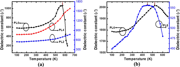
Figure 4. (a), (b) Temperature-dependent dielectric constant (ε') of PL10x measured at 1 kHz frequency.
Download figure:
Standard image High-resolution imageThe ferroelectric behavior with the DPT phenomenon of the dielectric materials can be explained by Curie-Weiss law above Tm [40]. The relationship for ε' with the temperature above Tm is given by equation (7).

Where; C is Curie-Weiss constant and T0 is Curie-Weiss temperature (Tc) for second-order phase transition and less than Tm for the first-order phase transition [41].
Figures 5(a)–(c) show the reciprocal of ε' with temperature for PL0, PL6 and PL8 thin films. As we fitted using equation (2), we observed T0 is above Tm for all thin films. We noticed the value of T0 is reduced for the higher doping on lanthanum. We observed a degree of deviation,  = 15, 50, and 70 for PL0, PL6 and PL8 respectively due to compositional induced diffuse phase transition behavior [21]. Where Tcw represents the temperature from which ε' begins to deviate. Some of the parameters calculated are shown in table 3.

Figure 5. Curie-Weiss behavior at 1 kHz in thin films (a) PL0 (b) PL6 (c) PL8 [Inset:  of their respective films].
Download figure:
Standard image High-resolution imageTable 3. Summary of calculated dielectric parameters of PL0, PL6 and PL8 thin films at 1 kHz.
| Parameter: | εm | Tm(K) | C(K) | Tcw(K) | Δcw (K) | γ |
|---|---|---|---|---|---|---|
| PL0 | 1064 | 575 | (71.25 ± 0.02) × 105 | 590 | 15 | 1.19 ± 0.05 |
| PL6 | 2016 | 525 | (34.13 ± 0.09) × 105 | 575 | 50 | 1.69 ± 0.05 |
| PL8 | 556 | 450 | (2.96 ± 0.04) × 105 | 520 | 70 | 1.95 ± 0.16 |
In addition, the modified Curie-Weiss law can also explain the DPT behavior of the relaxor materials related by equation (8) [42]. Where, γ provides DPT behavior and C' is Curie-Weiss like constant.

For γ = 1, a normal Curie-Weiss law is obtained, and γ = 2 describes a complete diffuse phase transition. The value of γ lies between 1 and 2 representing incomplete diffuse phase transition of the materials [41]. γ = 1 denotes normal ferroelectric material whereas 2 represents complete phase transition behavior of relaxor materials.
The fitting with an equation (8) is shown in figures 5(a)–(c) inset, at 1 kHz frequency for PL0, PL6 and PL8 thin films. We obtained γ as 1.19 ± 0.05, 1.69 ± 0.05 and 1.95 ± 0.16 indicating that PL6 and PL8 thin films exhibit incomplete diffuse phase transition. Thus, on increasing Lanthanum concentration such behavior is dominant than undoped or lower doped of lanthanum. It also indicates that dopants with La3+ ≥ Sc3+ increase the DPT of the materials.
As we observed the DPT of PL6 and PL8 thin films, where ε'm decreases and Tm shifts towards higher temperature with increasing frequency. Furthermore, we analyzed the frequency dependency of Tm by using the Vogel-Fulcher relation given in equation (9) [43].

Where; f0 is the pre-exponential factor, TVF is the characteristic Vogel-Fulcher freezing temperature, Ea is the activation energy and kB is Boltzmann's constant [44, 45].
The reasonably well fitted non-linear curve shown in figure 6, yielded f0 ∼ 106 Hz, TVF = 477 K and 411 K and factor, Ea = 0.031 eV and 0.054 eV respectively and are physically acceptable values [46]. These are in good agreement with the earlier reports on Pb(Zr0.53Ti0.47)0.60(Fe0.5Ta0.5)0.40O3 [47]. The earlier report on Pb(Zr0.53Ti0.47)0.90Sc0.10O3 had shown Ea = 0.037 eV and f0 = 1.538 × 10⁶ Hz [16]. Thus, analysis of Vogel-Fulcher relation, further supports PL6 and PL8 thin films behave disorder ferroelectric, typically called relaxor ferroelectric materials. In addition, one can notice a comparatively slim polarization electric field (P-E) hysteresis loop of those thin films which suggest higher content of lanthanum on PZT strengthen the spontaneous polarization.

Figure 6. Vogel-Fulcher relation in the frequency range of 0.1–100 kHz of (a) PL6 and (b) PL8 thin films.
Download figure:
Standard image High-resolution imageFigures 7(a)–(e) show the Cole-Cole plots of the temperature-dependent dielectric permittivity of the real (ε') and imaginary (ε'') part of PL10x thin films at frequency range 102–106 Hz. We observed some characteristics of ε' versus ε'' response for PL10x thin films in the temperature ranges 100–650 K. (i) The ε' radius of the semicircular arc shows high variation with temperature, (ii) With increasing temperature the bulk permittivity contribution (ε' radius, when ε'' = 0) in the Cole-Cole plot increases, since the intercept of the semicircular arc gives an estimation of sample resistance, this indicates that the resistance increases from PL0 to PL6 and again decreases for PL8. The incorporation of the La3+ and Sc3+ ions could be responsible for change in its conduction properties [36, 48]. These dopants are mainly of two types: La3+ is a donor dopant that produces a soft PZT and Sc3+ is an acceptor dopant that produces a hard PZT. In addition, the decrease in the resistance for PL8 is due to higher doping of Lanthanum compared to scandium may facilitate the domain wall motion [49, 50]. (iii) the samples exhibit multi-dispersive relaxation time on increasing the temperature. Two intercepts between the real axis ε' and the circular arc, assign for the static dielectric constant, εs (largest value ε' radius, when ε'' = 0) and the optical dielectric constant, ε∞ (smallest value ε' radius, when ε'' = 0) were observed in all samples which increased on doping compounds, this large increase is due to the variation of the domain wall motion that affects the resistance of the compound. These observed changes in the shape of Cole-Cole plots of dopant films could be due to different strains, that are produced by the different sizes of the doping ions that produce a variation of the dielectric and conductivity properties of the materials [51, 52],.

Figure 7. (a)–(e) Show Cole-Cole plots of the temperature-dependent dielectric permittivity real part (ε') versus imaginary part (ε'') for PL10x thin films.
Download figure:
Standard image High-resolution image3.3. Ferroelectric properties
The energy storage performance of ferroelectric materials is one of the key indicators for evaluating materials engineering applications. It can be estimated using unipolar P-E loops under the external applied electric field. According to the definition of energy-storage density using P-E hysteresis loops, the stored energy per unit volume (Ust) and the recovered energy per unit volume (Ure) are given by [53]


Where; E is the applied electric field, P is the displacement charge density for ferroelectric materials, and Pr is the remnant polarization, Pm is the maximum polarization. Evidently, based on equations (10) and (11), the value of Ust and Ure can be easily obtained by numerical integration of the area between the polarization axis and the curves of the P-E loops. To estimate these values, we analyzed the positive branch of P-E curve and calculated the energy storage efficiency (η) as

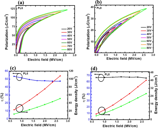
Figures 8(a)–(e) shows temperature-dependent (100–500 K) P-E hysteresis loops of PL10x thin film measured under an applied electric field of 0.67 MV cm−1 electric field at 1 kHz frequency. Reproducible and stable ferroelectric loops with slight changes in polarization and coercive field were observed for all thin films. From the comparative graph of PL10x thin films as shown in figure 8(f), we observed typical ferroelectric loops with enhanced polarization and reduced coercive field for PL2 and PL4 thin films. Furthermore, PL6 and PL8 show slim loop hysteresis with high ΔP (Pm–Pr). These changes in parameters of the hysteresis loop were due to the substitution of scandium and lanthanum in PbZr0.53TiO.47 (PZT). We estimated the energy storage capacity at 300 K for the same applied electric field (0.67 MV cm−1) for PL10x thin films, achieving enhanced Ure, Ust and η due to doping elements. The estimated Ure value estimated was the greatest ∼12.24 with η = 53.4% for PL6. But we had better η = 66.67% with Ure = 4.82 J cm−3 for PL8 thin films. All the calculated parameters are summarized in table 4. Considering energy storage capacity and efficiency, we further, analyzed the positive branch of P-E loop for possible energy storage applications. Figures 9(a), (b) show the room temperature unipolar P-E hysteresis loops of PL6 and PL8 thin films measured under various applied electric fields at 2 kHz of frequency. The slim loop of these thin-film capacitors revealed relaxor ferroelectric behavior in PL6 and PL8 in line with dielectric results. We observed slight asymmetries at positive and negative branches in the hysteresis loop of PL6 and PL8 films that could be due to different work functions of top (Pt) and bottom (LSMO) electrodes [54, 55]. In addition to the layer interface effect which acts as pinning centered, defect-related oxygen vacancy and impurities might be also responsible for the observed asymmetry hysteresis loop [56, 57].

Figure 8. Temperature dependent P-E hysteresis loops of thin films measured under applied electric field (0.67 MV cm−1) at frequency 2 kHz (a)–(e) and P-E hysteresis loop of various composition (f) at 300 K.
Download figure:
Standard image High-resolution imageTable 4. Summary of ferroelectric and energy storage parameter of PL10x thin films under 20V (0.67 MV cm−1) at 2 kHz frequency.
Parameter:
| Pr (μC cm−2) | Pm (μC cm−2) | EC (kV cm−1) | Ure (J cm−3) | Ust (J cm−3) | η (%) |
|---|---|---|---|---|---|---|
Sample 
| ||||||
| PL0 | 24.4 | 35.3 | 187 | 1.26 | 14.37 | 8.76 |
| PL2 | 35.3 | 65.1 | 103 | 6.27 | 19.39 | 32.01 |
| PL4 | 26.4 | 61.1 | 50 | 6.38 | 15.99 | 39.89 |
| PL6 | 9.6 | 71.9 | 152 | 12.24 | 22.92 | 53.4 |
| PL8 | 3.6 | 19.2 | 50 | 3.82 | 5.73 | 66.67 |
Figure 9. (a), (b) P-E hysteresis loops of thin films PL6 and PL8 (c), (d) η of thin films PL6 and PL8 and their respective Ure (green color) and Ust (red color) at the right of y-axis measured at the various applied field at frequency 2 kHz.
Download figure:
Standard image High-resolution image
Near the breakdown electric field (∼2.67 MV cm−1) at 2 kHz frequency, the enhanced polarization Pr ∼ 46.6 μC cm−2 and Pm = 125.4 μC cm−2, consequently yielded  and reduced Ec ∼205 kV cm−1 were obtained for PL6 films. In the similar applied electric field, for PL8 films Ec was further reduced to 12 kV cm−1 and Pr ∼ 8.4 μC cm−2 and Pm ∼ 39.2 μC cm−2, achieved ΔPm = 4.66, which resulted in slimmer P-E loop strengthening η. Thinner P-E loops were achieved in our films than undoped PbZr0.53Ti0.47O3 (PZT) [58], PbZr0.40Ti0.60O3 [59] films which were expected. It is obvious that higher ΔPm would better to achieve enhanced η.
We estimated Ure, Ust and η for PL6 and PL8 films from their respective P-E loops. It turns out to be Ure = 51.15 J cm−3 Ust = 107.95 and η = 47.38% at an applied electric field of 2.67 MV cm−1 and frequency 2 kHz for PL6 thin films which is in good agreement with  where EBD is electric breakdown strength PL6 possesses higher ε' and high breakdown strength. The obtained values of PL6 are comparable with slightly less η as reported in Pb0.91La0.09(Zr 0.35Ti0.65)O3 thin films, Ure ∼ 28.7 J cm−3 with η ∼ 57% [60]. We thus achieved enhanced energy values than the studies on oriented Pb(Zr0.52Ti0.48)O3) thin films, that had shown Ure ∼ 8 J cm−3 and η ∼79.6% under an applied electric field of 0.8 MV cm−1, synthesized by chemical solution method [61]. On the other hand, Nguyen et al had reported [62] η ∼ 13.7 J cm−3 and a η ∼ 88.2% at 1 kV cm−1 in 10% La-doped epitaxial PLZT thin films grown on SRO/STO/Si substrates using pulsed laser deposition. By comparing with this result, we have achieved higher Ure = 26.54 J cm−3 but with slightly less η = 65.88% for PL8 thin films under an applied electric field 2.67 MV cm−1 and frequency of 2 kHz. The energy storage performance of our thin films showed higher breakdown strength and better Ure as compared to BaZr0.20Ti0.80O3 (BZT) thin films showing Ure = 21.28 J cm−3 and η = 83.51% [63], however, these films have shown enhanced and better energy storage capacity for multilayer Pb(Zr0.4Ti0.6)O3/BaZr0.2Ti0.8O3/Pb(Zr0.4Ti0.6)O3 (PZT/BZT/PZT), thus these materials might be useful for making sandwich structure to achieve high energy density capacitors. We observed Ure and Ust of PL6 and PL8 thin films are directly proportional to the applied electric field. However, η is slightly decreased with an increase in an electric field is expected as reported by 0.942[Na0.535K0.48NbO3]−0.058LiNbO3 (KNNLN) films [64]. The summary of the estimated value of ferroelectric functionalized parameters of PL6 and PL8 thin films is given in table 5.
Table 5. Summary of calculated values of energy storage parameters of PL6 and PL8 thin films measured under various electric fields at 2 kHz frequency.
Sample:
| E (MV cm−1) | .67 | 1 | 1.33 | 1.67 | 2 | 2.33 | 2.67 |
|---|---|---|---|---|---|---|---|---|
| PL6 | Ure (J cm−3) | 12.24 | 17.64 | 23.1 | 29.15 | 36.02 | 43.21 | 51.15 |
| Ust (J cm−3) | 22.92 | 34.27 | 46.73 | 60.73 | 75.22 | 92.12 | 107.95 | |
| η | 53.4 | 51.48 | 49.43 | 47.99 | 47.88 | 47.38 | 47.38 | |
| PL8 | Ure (J cm−3) | 3.82 | 6.67 | 9.94 | 13.67 | 17.84 | 22.22 | 26.54 |
| Ust (J cm−3) | 5.73 | 9.98 | 14.79 | 20.59 | 26.52 | 33.48 | 40.28 | |
| η | 66.67 | 66.83 | 67.21 | 66.73 | 67.26 | 66.36 | 65.88 |
4. Conclusion
The XRD patterns of (PbZr0.53Ti0.47)(1−y)(LaxSc1−x)yO3 thin films revealed highly oriented (100) films with the perovskite phase. The dielectric data revealed an increase of dielectric permittivity when lanthanum content increased by 6%, however, a further increase of lanthanum (8%) resulted in the reduction of dielectric constant. We further noticed the role of increasing lanthanum contents (decreasing scandium) resulting in broadening of dielectric permittivity with temperature and ferroelectric phase transition from 575 K to 450 K. It clearly indicated that analysis of modified Curie-Weiss law for the thin films PL6 and PL8 behave relaxor-ferroelectric which further supported by Vogel-Fulcher relation. Cole-Cole plot analysis showed the samples exhibit multi-dispersive relaxation time on increasing the temperature. In addition, a large increase in the resistance of the samples was observed when the amount of the lanthanum dopant was increased because the lanthanum modifies the domain wall motion in the samples.
The polarization electric field (P-E) plot exhibits the role of lanthanum and scandium causes a substantial reduction in coercive fields. Furthermore, enhanced polarization was achieved on PL2, PL4 and PL6 thin films. In addition, PL6 and PL8 thin films show the slim loop P-E curve, which indicates a relaxor-ferroelectric nature. We achieved Ure = 51.15 J cm−3 with η = 47.38% for PL6 under 2.67 MV cm−1 at 2 kHz frequency and η = 65.88% with Ure = 26.54 J cm−3 for PL8 thin films. The study confirms the idea that, by tuning La3+ and Sc3+, the dielectric and ferroelectric functional properties of thin films can be controlled for better memory, power electronics, and energy storage devices.
Acknowledgments
This work was financially supported by DoD Grant #FA9550-20-1-0064. M. Bhattarai acknowledges receiving financial assistance from the PR NASA EPSCoR, Grant # 80NSSC19M0049. The authors would like to thank MSRC characterization facilities Cupey, San Juan PR for XRD measurements.
Data availability statement
All data that support the findings of this study are included within the article (and any supplementary files).