
Abstract
Theoretical and experimental results indicate that naturally the ultrathin nanofilms of some wurtzite (WZ) semiconductors will transform into a stable nonpolar graphitelike structure from the polar surface. Normally, the thicknesses are just limited to a few atomic layers. By epitaxial tensile strain, the thickness can be extended. In this work, employing the first-principles calculations focus on WZ materials ZnO, BeO, SiC, GaN, InN and AlN, we predicted that under a certain pressure with a weak electric field, their thickness range of forming graphitic nanofilms is greatly enlarged. This research provides theoretical guidance for the synthesis of new two-dimensional (2D) structures.
Export citation and abstract BibTeX RIS

Original content from this work may be used under the terms of the Creative Commons Attribution 4.0 licence. Any further distribution of this work must maintain attribution to the author(s) and the title of the work, journal citation and DOI.
1. Introduction
Graphene has fascinated a lot of attention for the excellent optical, electrical, mechanical, and thermal properties since it was synthesized [1–3], which has important application prospects in materials science, micro-nano processing, energy, biomedicine and drug delivery. It is considered to be a revolutionary material in the future. Graphitelike 2D materials have similar structures to graphene, which may also have some distinctive physical properties and attracted widespread interest [4–7]. Previous theoretical [8] and experimental [9] researches have shown that (0001) oriented ultrathin nanofilms of WZ materials can spontaneously relax into a stable graphitelike structure. In the graphitelike phase, the cations and anions are arranged in a trigonal-planar coordination, so as to remove the intrinsic surface dipoles to stabilize the film. However, this transformation is just limited to a certain number of layers. Therefore, some method such as epitaxial tensile strain has been proposed to extend the thickness range [10].
In this work, based on first-principles calculations, we propose a new method to extend the thickness range of the graphitelike nanofilms of WZ materials. By applying a weak electric field perpendicular to the surface under a certain pressure on WZ films, the thickness range is significantly enlarged. And the larger the applied electric field and the pressure, the thicker the layers. Normally, utilizing the electric field to tuning some physical properties such as topological phase transition [11], spin interactions [12], optical performance [13], electronic properties [14], and Curie temperature [15], etc. The magnitude of the electric field is usually V/Å. However, in this research, to tuning the thickness of forming graphitelike nanofilms, under a certain pressure, we just applying a magnitude of V/m electric field to achieve this manipulation.
Under a certain pressure on WZ films, the lattice constants are stretched. As for the interactions between the cations and anion, the cations move toward the internal layers and the anions go toward the surface. It leads to the WZ phase tends to form the graphitelike structure.
2. Computational methods
To simulate the (0001) surface of WZ materials, we construct a set of slabs for ZnO, BeO, SiC, GaN, InN, and AlN, and the vacuum space of 20Å is added in the direction of the c-axis to avoid the interactions between layers. All the supercells are periodically repeating in three dimensions. The first-principles calculations are carried out within the framework of density functional theory (DFT) by using the Cambridge Sequential Total Energy Package (CASTEP) [16]. The exchange-correlation function adopts the Perdew–Burke–Ernzerhof (PBE) of the generalized gradient approximation (GGA) [17]. The ultrasoft pseudopotentials [18] and the plane-wave cutoff energy of 480 eV are used for geometry optimization. The reciprocal space scheme utilized the Monkhorst-Pack k-grid [19] 20 × 20 × 1 in the Brillouin zone. To ensure the convergence of optimization, the energy criteria are set to be 2 × 10⁻⁶ eV atom−1.
In the geometry optimization with an electric field under a certain pressure, to obtain the numbers of forming graphitelike layers, there are two methods. The first one is that cutting a WZ slab, and applying the electric field and pressure. Then fully relax it until the convergence to check whether the WZ structure has transformed into a graphitelike structure. This method needs to test multiple times for slabs of different thicknesses, so it is expensive and time-consuming. The second one is that creating slabs of WZ and graphitelike structures in thinner layers, respectively. For the slabs of WZ structures, the atom positions and the lattice constants along the c-axis are fixed. For the slabs of graphitic structures, we just constrain the lattice constants along the c-axis and all the other structural parameters are fully relaxed. Finally, we can obtain the energy and surface area of WZ and graphitelike slabs. And then increase the thickness and repeat the calculations. From the above data, we can depict the image of the cleavage energies as a function of film thickness for WZ and graphitelike slabs. Finding the intersection of the two curves, the layers of forming graphitelike structure can be obtained. In this study, we employ the latter method. About the validity of the linear relationship between cleavage energy and number of layers as increasing the number of layers, we have tested the results using the direct optimization method and the finding intersection method for a serial of wurtzite semiconductors. The results indicate that the maximum number of layers of forming graphitelike phase are the same by the two calculation methods. Therefore, it is reasonable to employ the second method to obtain the maximum number of layers of forming graphitelike phase.
3. Results and discussion
For demonstration, we choose ZnO as an example and depict the slabs in figure 1. As shown in figure 1(a), the WZ structure stacked alternating hexagonal lattice planes composed of tetrahedral-coordinated cations and anions along the c-axis [10]. So cleaving the (0001) films creates two cases: a cation-terminated or an anion-terminated surface, which are so-called polar surfaces [20]. This structure leads to a divergence of the surface energy that makes the surface intrinsically unstable [8]. By natural relaxation, within a few atomic layers thick, polar WZ structure can be transformed into a nonpolar graphitelike structure, in which cations and anions are threefold coordinated in flat hexagonal sheets [21, 22], as shown in figure 1(b).
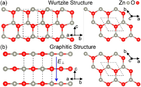
Figure 1. Side and top view of ZnO film in (a) WZ structure. (b) Graphitelike structure. Blue arrow indicates the direction of the perpendicular electric field.
Download figure:
Standard image High-resolution imageWe calculate the cleavage energies (Ecleavage) of ZnO, BeO, SiC, GaN, InN, and AlN slabs in WZ and graphitic structures under the pressure of 4 GPa with 50 V m−1 electric field according to the formula:

where Eslab indicates the energy of the slab, Ebulk means the bulk energy and A denotes the area of the two surfaces after optimization [8]. The calculated results are plotted in figure 2. The blue and red dotted line represents the cleavage energies of WZ and graphitic slabs in the different number of layers. As shown in it, the cleavage energies vary linearly with the number of layers. They cross at a certain thickness, which is corresponding to the critical thickness of forming graphitelike slabs. Below this number of layers, the slabs employ graphitic structure and beyond this value, the WZ structure is more stable. Because it has lower cleavage energies. For comparison, we listed the maximum number of layers up to the graphitic structure for the above mentioned six WZ materials in table 1. Row a and b gives the maximum number of layers obtained from works of literature [8, 10], row d lists our calculation results and they are in well agreement with the available data. Row c summarizes the maximum number of layers with 5% tensile strain [10] and we also repeat this calculation and find with 7% tensile strain, the results of ZnO slabs are the same as those in [10], so we apply 7% tensile strain for the six WZ films and list the results in row e. For the nanofilms of BeO and AlN, our results are smaller, For the InN slab, the calculated number of layers is larger. The other results coincide with each other. Row f gives the maximum number of layers for (0001) slabs just with a perpendicular electric field, the data in the parentheses are the corresponding voltage that needs to provide. From which we can see that to obtain a larger thickness of forming graphitelike surface, it needs to provide an electric field of the order V/Å. However, it is difficult to achieve in experiment. The data in row g are the number of layers for (0001) slabs under the pressure of 4 GPa. Relative to the natural relaxation, the maximum number of layers of forming graphitelike phase is significantly improved, so a larger number of layers are expected if continue to increase the pressure. Row h are the obtained results for (0001) slabs under the pressure of 4 GPa with a perpendicular electric field of 50 V m−1. Compare row g and h, we find that under the pressure of 4 GPa, except for the harder SiC and GaN nanofilms, the number of layers of the other four slabs are increased with a weaker electric field of 50 V m−1. The largest increase happens in the BeO slab, which is from 32 layers to 46 layers. This indicates that for some WZ films, a weaker electric field under a certain pressure can promote the forming of a thicker graphitelike structure. For SiC and GaN nanofilms, a larger electric field and pressure are expected to improve the number of layers. Because we find that the maximum number of layers of forming graphitelike phase increases with the increasing of electric field and pressure. About this point, we discuss in detail in figure 3.

Figure 2. (a)–(f) Cleavage energies as a function of film thickness for ZnO, BeO, SiC, GaN, InN, and AlN in WZ and graphitic structures under the pressure of 4GPa with 50 V m−1 electric field.
Download figure:
Standard image High-resolution imageTable 1. Maximum number of layers up to the graphitic structure is stable relative to the WZ structure.
| Film | ZnO | BeO | SiC | GaN | InN | AlN |
|---|---|---|---|---|---|---|
| a | 18 | 30 | 8 | 12 | — | 24 |
| b | 16 | 28 | 6 | 10 | 8 | 22 |
| c | 32 | 48 | 8 | 16 | 20 | 48 |
| d | 16 | 26 | 6 | 8 | 10 | 22 |
| e | 32 | 30 | 6 | 14 | 26 | 36 |
| f | 20 | 44 | 10 | 18 | 16 | 26 |
| (V/Å) | (0.20) | (0.50) | (0.06) | (0.26) | (0.12) | (0.40) |
| g | 30 | 32 | 10 | 14 | 16 | 32 |
| h | 34 | 46 | 10 | 14 | 24 | 36 |

Figure 3. Film thickness as a function of the electric field under the pressure of 1–4 GPa for ZnO (0001) nanofilms.
Download figure:
Standard image High-resolution imageTo investigate the effect of the electric field and the pressure on the structure of WZ nanofilms in detail, we further study the variation of the lattice constants and the total energy of graphitic and WZ nanofilms under the pressure of 4 GPa with 50 V m−1 electric field. 6-layer slabs are chosen for the six WZ semiconductors and the results are summarized in table 2. The value in the parentheses is the variation ratio relative to the original lattice constants. It means elongation if the ratio is positive and a negative value indicates contraction. From table 2, we can see that the lattice constants of the slabs in WZ and graphitic structures are both stretched. For the graphitelike films, the tensile effect is more significant, which results in the larger area of the surface and is consistent with the conclusion that the tensile strain is the benefit to extend the thickness range of stable graphitic films [10]. Besides, the total energy of the unit cell of graphitic films is lower than that of WZ films. So for 6-layer slabs, the lower cleavage energy of the graphitic phase comes from the larger surface area and the lower total energy. With the increase of the layers, it needs a larger electric field and pressure to sustain the stable graphitic structure.
- a.Theory results by CASTEP code in [8].
- b.Theory results by VASP code in [10].
- c.Theory results by VASP code with 5% tensile strain in [10].
- d.Our calculation results in natural relaxation.
- e.Our calculation results with 7% tensile strain.
- f.Our calculation results with a perpendicular electric field, which is given in the parentheses.
- g.Our calculation results under the pressure of 4 GPa.
- h.Our calculation results under the pressure of 4 GPa with a perpendicular electric field of 50 V m−1.
Table 2. The lattice constants and the total energy of 6-layer WZ and graphitic nanofilms under the pressure of 4 GPa with 50 V m−1 electric field, the data in the parentheses is the variation ratio relative to the original lattice constants.
| Wurtzite structure | Graphitic structure | |||
|---|---|---|---|---|
| a (Å) | E (103 eV) | a (Å) | E (103 eV) | |
| ZnO | 3.364 | –5.152 | 3.457 | –5.153 |
| (3.5%) | (6.4%) | |||
| BeO | 2.733 | –1.408 | 2.748 | –1.410 |
| (1.3%) | (1.9%) | |||
| SiC | 3.147 | –0.779 | 3.152 | –0.782 |
| (2.2%) | (2.4%) | |||
| GaN | 3.221 | –6.970 | 3.274 | –6.971 |
| (1.0%) | (2.7%) | |||
| InN | 3.609 | –5.490 | 3.709 | –5.491 |
| (2.0%) | (4.8% | |||
| AlN | 3.124 | –0.986 | 3.220 | –0.988 |
| (1.1%) | (3.5%) | |||
To demonstrate the effect of the electric field under a certain pressure on the maximum number of layers of forming graphitelike phase, we choose ZnO (0001) nanofilms as an example. The results of other wurtzite materials are similar to those of ZnO. We calculated the maximum number of layers in the different electric fields under the pressure of 1 to 4 GPa and the results are plotted in figure 3. From figure 3, we find that under the pressure of 1 GPa, the tuning effect of the electric field on the number of layers has not been observed. However, by applying a certain pressure perpendicular to the surface of the ZnO (0001) slab, the maximum number of layers of forming graphitelike phase is increased relative to those in natural relaxation. It increases from 16 or 18 layers to 24 layers. And with the increase of the pressure, the effect of the electric field on the number of layers appears. Under 2 GPa, the maximum number of layers is increased to 26 layers without the electric field. When the electric field ranges from 50 V m−1 to 100 V m−1, a platform appears. Subsequently, it increases to 30 layers at 200V m−1. Similar platforms are also observed at the pressure of 3 and 4 GPa, the difference is only that with the increase of the pressure, the width of the platform becomes narrow or even disappears. A new higher platform generates with a larger electric field under higher pressure. The larger the pressure, the more sensitive the tuning effect of the electric field. Because under the electric field, the direction of the electric field force on the cations toward the inner of the slab and that on the anions toward the surface. It is benefit to form the graphitelike structure. If only the electric field is applied, to achieve this effect, the magnitude of the needed electric field is usually V/Å. However, under a certain pressure, the effect of the pressure on the forming of graphitelike phase weakened the needed electric field, so the magnitude of the electric field is just V/m.
Under the pressure of 4 GPa with a 50 V/m voltage, the Mulliken charge distribution and the bond length of the anions and cations for the 6-layer slabs in WZ and graphitic structure are depicted in figure 4. From which, we observe that a 6-layer nanofilm becomes a 3-layer film. In this process, they change into a flat graphitic structure to remove the destabilizing dipole [8]. The size of charge transfer between cation and anion in the outmost layer varies from 0.09e/0.14e (ZnO) to 0.39e/0.35e (SiC) in the WZ phase. For graphitelike phase, that varies from 0.01e (BeO) to 0.06e (InN,GaN, AlN). The polarization of the bonds between cation and anion is significantly weakened in the graphitelike phase relative to those in the WZ phase. Without the electric field and pressure, the charge transfer ranges between 0.05e (ZnO) to 0.27e (SiC) in graphitic (0001) surface [8]. Namely, the electric field under a certain pressure enhances the charge transfer to the anions in surface layers and affects the removal of the dipole. This mechanism is benefit to forming the graphitelike structure. In the process of structural phase transition, the charge of the anion in the inner layer almost changes little, which is close to that in the bulk WZ semiconductors. Large charge transfer happens between the cations in the inner layer and the anions in the surface layer.

Figure 4. (a)–(f) Mulliken charges distribution and the bond length of the anions and cations for the 6-layer slabs in WZ and graphitic structure under the pressure of 4 GPa with 50 V m−1 electric field.
Download figure:
Standard image High-resolution image
Compare the effect of strain and the electric field under a certain pressure, we notice that strain has minimal affection on charge transfer in both WZ and graphitic films. For WZ structure, the charge transfer is mainly confined in the surface layers from anion to cation. And for flat graphitic structure, there is no charge transfer involved in the surface stabilization [10]. However, under the pressure of 4 GPa with 50 V/m voltage, we observed an interesting phenomenon. For the WZ structure, the charge difference between cation and anion in the outmost layers is larger than that in the inner layer. It means the polarity of the chemical bonds in the surface layer is stronger. For the graphitic structure, the charge difference between cation and anion in the outmost layers is smaller than that in the inner layer. It indicates that the polarity of the chemical bonds in the surface layer is weaker. For example, in WZ SiC film, the charge difference between Si and C in the surface layer is 0.39e/0.35e, and that in the inner layer is 0.05e. In graphitic SiC film, the charge difference between Si and C in the surface layer is only 0.03e, while that in the inner layer is 0.07e. The polarity of the chemical bonds in the interior is stronger. Similar results can be found in the other compounds. Therefore, we think that thicker layers of forming graphitic phase in the electric field under a certain pressure may be caused by this abnormal charge transfer. By calculations we found that there exists a threshold pressure for the enhancement of charge transfer. Below a certain pressure, the effect of the electric field is very weak. And beyond a certain pressure, the affection of the electric field will appear. Moreover, the harder the materials, the larger threshold pressure.
The geometry transform results in the surface atoms changes from sp3 tetrahedral toward sp2 trigonal planar coordination as the surface-layer cations contract inwards toward the interior layers and the anions in the second layer move towards the surface [8]. After relaxation, the average distance between layers increased compared to that in the WZ structure. The length of the bonds between cation and anion in the same layer is reduced. For example, in ZnO nanofilms, the bond length of Zn-O is 1.995Å, which contracts by 13% compared to 2.035Å in WZ films. The separation between the layers increased from 2.035Å to 2.569Å, it is larger 26%. However, in natural relaxation, the distance between layers is increased by 20%. Namely, this variation is more significant in the slabs by applying the electric field and pressure, which leads to the interaction between the layers is weakened. The graphitelike films are insulating and the WZ films are metal. The two structures can realize mutual conversion by some regulation methods such as applying strain, electric field or pressure, etc
4. Conclusion
In summary, employing first-principles calculation, we studied the (0001) nanofilms of six typical WZ compounds ZnO, BeO, SiC, GaN, InN, and AlN. Their cleavage energies in WZ and graphitic structures under the pressure of 4 GPa with 50 V m−1 electric field are calculated to find the maximum number of layers up to the graphitic structure. For comparison, we list the limited number of layers by different tuning methods. Also, for demonstration, the variation of the maximum number of ZnO (0001) nanofilms with the voltage and pressure is plotted. The Mulliken charges distribution, the lattice constants, and the total energy of 6-layer slabs under the pressure of 4 GPa with 50 V m−1 are analyzed. In the above research, we propose a novel and feasible idea to grow thicker graphitelike nanofilms based on WZ semiconductors. This method only needs to provide a weaker electric field under a certain pressure, which is simple and easy to achieve. We hope this work could provide some guidance for the experiment.
Acknowledgments
This work is supported by State Key Laboratory of Advanced Technology for Materials Synthesis and Processing (Wuhan University of Technology, 2021-KF-16), the Fundamental Research Funds for the Central Universities (WUT: 2020IB010) and National Natural Science Foundation of China under the Grant No. 61575085, 61240056.
Data availability statement
The data that support the findings of this study are available upon reasonable request from the authors.