
Abstract
We describe a method for phase separating and transferring block copolymer (BCP) nanoscale patterns to arbitrary substrates for surface-independent nanolithography. The enabling technology is a hydrogenated or oxidized graphene thin film that only weakly adheres to its substrate. BCPs are applied to these graphene-based materials and solvent annealed to effect nanoscale phase separation. Then, taking advantage of the weak interaction of the graphene film and its substrate, the BCP/graphene stack is delaminated easily in water. A target substrate is then used to retrieve the stack, which can then serve as a lithographic mask. The use of water as a lift-off agent allows for chemically mild retrieval of the phase-separated BCP, extending the BCP lithography technique to essentially arbitrary substrates. We demonstrate this graphene-enabled BCP lithography on silicon nitride and polyethylene. We also show that using reduced graphene oxide (RGO) as a thin film enables the transfer of wafer-scale BCP films and lithography on SiOx and Si. We use an RGO support to produce phase-separated BCP solvent-annealed patterns on polystyrene, a result which is not possible using standard BCP solvent annealing and which shows the utility of this technique. Finally, we demonstrate the ability to create nanopatterns of higher complexity by stacking multiple BCP masks, a capability that is not possible using conventional BCP lithography. This technique may have applications in fabricating nanoporous membranes and photonically active coatings.
Export citation and abstract BibTeX RIS
1. Introduction
Block copolymer (BCP) films exhibit nanoscale phase separation on the order of 10–100 nm [1, 2]. This property has attracted a great deal of interest because it opens up the possibility of top-down patterning of materials at the nanoscale. In particular, a technique known as BCP lithography has been developed to take advantage of this possibility [3]. BCP lithography involves coating a surface with BCP, effecting the nanoscale phase separation, and using the variable-thickness phase-separated polymer as a mask for etching the underlying substrate [4]. Depending on conditions of polymer preparation, phase separation, and substrate surface functionalization, the patterns can exhibit a range of morphologies, with circular lattices, lines, and more complex shapes emerging as possibilities [5, 6]. BCP lithography therefore represents a powerful tool for facile generation of nanoscale patterned structures on surfaces. These surfaces may find use in microelectronics fabrication, membrane fabrication for nanofiltration, and photonic materials design and synthesis, among other applications [6, 7].
Despite its promise, a significant roadblock for BCP lithography is the sensitivity of the BCP nanoscale phase separation to the chemical makeup of the surface to be etched. This often necessitates preparation of the surface, methods of which include chemical and photolithographic pre-patterning and covalent grafting of random copolymers to ensure that the BCP wetting properties of the surface are optimal [8, 9]. In light of the wide variety of materials used in modern electronics, the need to develop surface preparation procedures that are specific to individual surface chemistries creates a bottleneck in developing BCP lithography into a microfabrication technique that can be applied generically across a range of materials.
In earlier work, we developed method for transferring chemically functionalized graphene from one substrate to another that is mild and compatible with a very broad range of substrates. Briefly, we showed that chemical hydrogenation of single layer graphene weakened the adhesion of the graphene to its substrate, allowing delamination of the material in water and relamination onto a new substrate [10]. Chemical functionalities, including alkyl and amino groups, that were initially present on the graphene were preserved during the transfer process; thus this technique enabled surface chemical functionalization of a substrate without actually having to perform chemistry on that substrate. Subsequent studies showed that the single layer hydrogenated graphene (SLHG) was mechanically strong enough to support small electronic and polymeric structures as well [11, 12].
Earlier work has shown that graphene and other materials can be effectively etched into nanopatterns using BCP lithography [13, 14]. In addition, the phase separation of BCPs on graphene has been examined for patterning purposes, [15, 16] and at least one group has reported transferring these BCP patterns to a substrate for subsequent lithographic processing [17]. In that report, the researchers used a wet etch method to remove a graphene oxide (GO) layer from a SiO2 preparative substrate by etching with hydrofluoric acid, a caustic and poisonous chemical. Here we present an alternative method of BCP lithography transfer, based on our mild water lift-off of SLHG. This method is compatible with essentially any substrate, the only requirement being that the new substrate can be immersed in water. We also report a modification of graphene oxide that allows for a similar water-based delamination and relamination. Graphene oxide is water-dispersible and abundant; therefore, its use as a BCP lithography platform can be extended to very large area applications where SLHG is impractical and cost-prohibitive.
2. Methods
2.1. Hydrogenated graphene preparation
Single layer graphene was grown via chemical vapor deposition [18] and transferred onto silicon/silicon oxide wafers using a standard polymer-supported copper etching process [19]. The graphene was then hydrogenated via the Birch reduction, a dissolving metal hydrogenation [20]. Briefly, single layer graphene was placed in liquid ammonia at −33 °C with 50 mg of Li metal. The mixture was allowed to react for 30 s and the reaction was then quenched slowly with ethanol. The wafer with SLHG was rinsed with acetone and isopropanol and dried under N2. This reaction has been shown to weaken the adhesion of graphene to its substrate and allow the transfer of chemical functionality from one substrate to another [10]. SLHG slowly loses hydrogen to the environment over a period of several weeks and therefore its weakened adhesion dissipates over time. Therefore we used SLHG within 1 week after preparation to ensure that its delamination properties remain robust [21].
2.2. Graphene oxide preparation
Graphene oxide was prepared from graphite via a modified Hummers method [22, 23]. A suspension of 8 g/l of graphite oxide in water was diluted by 50% (v/v) with methanol and spin-coated at 900–3000 rpm or drop-cast onto a hydrophilic plasma-cleaned glass surface. The graphene oxide was then either thermally or chemically reduced [24]. Thermal reduction consisted of heating the graphene oxide to 250 °C in air for 30 s. Chemical reduction consisted of exposing the graphene oxide to hydrazine vapor in a small chamber for 15 min. RGO is significantly more stable than SLHG in an ambient environment; however, we also ensured that the RGO films were used within a week after their preparation. The thickness of the thermally reduced GO membranes used in this work is typically 20 nm, with a surface roughness of ± 5 nm, whereas the thickness of chemically reduced GO membranes is typically 25–30 nm with a roughness of roughly ± 7 nm. Thus, the roughness has a relatively small effect on the overall quality of the transfer and etching [24].
2.3. BCP thin film preparation
The BCP polystyrene-b-poly(2-vinylpyridine) (PS-b-P2VP, Mn = 135 and 53 kg mol−1 for PS and P2VP, respectively, and PDI = 1.18) was purchased from Polymer Source, Inc. and used as received. A 1 w/v% solution of PS-b-P2VP in toluene is spun onto the graphene transfer layer at 4000 rpm for 1 min This yields a BCP film with a thickness of approximately 40 nm. The BCP on SLHG or RGO then undergoes a static solvent vapor anneal: the sample is annealed in tetrahydrofuran (THF) vapor for 5–10 min by placing samples in a sealed vessel above a small amount of liquid THF at room temperature. This solvent annealing step phase-separates the PS and P2VP blocks into an array of dots [25–27]. Solvent annealing for longer time periods—up to 45 min—provides a structure of cylinders lying parallel to the surface of the substrate (hereafter referred to as 'parallel cylinder') by merging arrays of dots [13, 28, 29]. The BCP/SLHG is then delaminated from its substrate by immersing it slowly in water. This layered structure delaminates in a single piece and generally remains flat and unwrinkled due to its conformity with the surface of the water [10, 24]. The sample is then relaminated onto the target substrate by retrieving it directly with the substrate from underneath. The hydrophobicity of the graphene forces water from the graphene/BCP structure and the substrate as the stack dries, and the graphene/BCP layer is observed to be relatively wrinkle-free after transfer. Unlike SLHG with no polymer support, which undergoes significant tearing on the micron scale upon relamination, [10] the BCP-supported SLHG and RGO membranes are substantially thicker and more mechanically robust, and microtearing is not observed. After transfer, BCP/SLHG is immersed in ethanol for 30 min to form pore structures. To ensure open-pore formation, a sample is etched with oxygen plasma (135W, 160 mTorr O2 under N2) for 2 min. With the BCP/RGO, the formation of pores is processed before delamination in water. After relamination onto a new substrate, the sample is then etched with oxygen plasma for 2 min to ensure open-pore structures.
2.4. Porous silicon nitride preparation with BCP mask
Relaminated, open-pore structures of BCP/SLHG or BCP/RGO were prepared on a silicon nitride substrate. The sample was then etched by a reactive ion etcher (RIE) (MARCH, Nordson) with a CF4/O2 atmosphere for 30 s, followed by additional oxygen plasma etching for 1 min to clean possible carbonaceous residues. The substrate was characterized by atomic force microscopy (AFM) (Cypher, Oxford Instruments).
2.5. Data collection and measurments
All AFM was performed on an Asylum Cypher atomic force microscope (Oxford Instruments) in tapping mode. Scanning electron microscopy (SEM) was performed on a LEO SEM Supra 55 (Zeiss). X-ray photoelectron spectroscopy (XPS) was performed using a ThermoFisher Nexsa spectrometer, with excitation on the Al Kα line at 1487 eV. XPS data analysis, including elemental analysis, was performed using the built-in routines in Thermo Avantage software.
3. Results and discussion
We present a schematic of our workflow in figure 1. Briefly, we prepare SLHG or RGO on a convenient surface, usually SiOx. We then deposit a BCP thin film onto the SLHG or RGO and phase-separate the BCP using solvent annealing. This phase separation segregates the BCP into two separate nanoscale blocks of each polymer. We then delaminate the BCP/graphene stack in water and relaminate onto an arbitrary substrate. The BCP remains phase-separated throughout the process since each block of BCP is essentially not soluble in water. Once the BCP/SLHG is relaminated, further selective swelling may generate patterns such as nanopores, and the material is then etched using conventional oxygen plasma or reactive ion etching. The etching proceeds more quickly through the thin regions of the BCP and into the underlying substrate. This fact accounts for the ability to use the BCP as a lithographic mask to transfer the phase-separated nanopatterns to the underlying substrate.
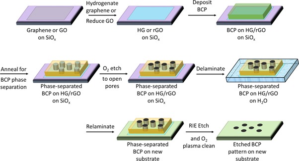
Figure 1. Schematic diagram of transferrable BCP lithography technique.
Download figure:
Standard image High-resolution imageWe observed well-separated nanoscale phases using polystyrene-block-poly(2-vinylpyridine) (PS-b-P2VP) as a representative BCP. The PS-b-P2VP was spun onto SLHG in a thin layer (See Materials and Methods) and phase separated using solvent annealing in THF for 5 min (figure 2(a)). This exploits the different solubilities of PS and P2VP in THF vapor; the phase separation is relatively fast [25]. This phase-separated BCP on SLHG is the patterned mask that could be subsequently delaminated in water for transfer onto new substrates. Figure 2(b) shows the surface morphology after relamination of the BCP/SLHG on the new SiO2 substrate. We observed that the phase separation is retained to a high degree of order after the transfer process. The sample was then soaked in ethanol for 30 min to form pores. In ethanol, the P2VP blocks will be collapsed onto the wall of the PS blocks and the underlying SLHG to generate porous PS films as shown in figure 2(c). Subsequent oxygen plasma etching was undertaken to degrade the phase-separated P2VP inside the pores as well as the SLHG underneath [25]. The final structures contain the open-pore PS film as shown in figures 2(d) and (e). The pores were on the order of 20–40 nm in diameter with a pitch of 24.6 ± 2.1 nm. We characterized the thickness of the final film after 2 min oxygen plasma etching (figure 2(d)) and the film thickness was approximately 25 nm, which is comparable to the measured pore depth. The final structure is typically hexagonal close packed P2VP pores, as shown in figure 2(e). We also observed a somewhat disordered pore network consisting of misaligned patches of hexagonal close packed P2VP pores (figure 2(e)). That misalignment is present both before and after delamination and relamination and may arise from either the heterogeneity of the graphene hydrogenation causing inhomogeneous adhesion of the polymer blocks across the surface of the material.
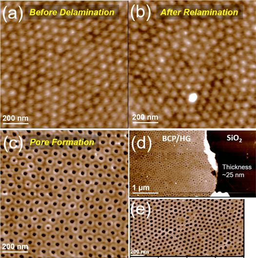
Figure 2. AFM height images of stepwise fabrication. (a) Phase separation before delamination of PS-b-P2VP on SLHG. (b) After relamination onto a new SiO2 substrate. The phase separation of the BCP is retained throughout the transfer. (c) Open pore formation of PS-b-P2VP block copolymer on SLHG by immersion in ethanol for 30 min (pore depth = 25 nm). (d) Image after subsequent oxygen plasma etching for 2 min to ensure open pores. The final thickness of our PS-b-P2VP/SLHG mask is approximately 25 nm. (e) High resolution image of the same sample in (d).
Download figure:
Standard image High-resolution imageFigure 3 shows results from the complete procedure carried out with SiNx as the target substrate of interest. We phase separated the BCP layer into two different patterns (pores and parallel cylinder 'fingerprints'). The fact that this transfer method allows us to etch two different BCP nanopatterns onto a substrate simultaneously illustrates the utility of the method. After phase separation and transfer to SiNx (figure 3(a)), the material was treated with a CF4 reactive ion etch (RIE) for 30 s. We observed a thin residue from the BCP mask after RIE, so we performed additional oxygen plasma etching followed by a sonication in acetone for 5 min to completely remove the residue (figure 3(b)). We used scanning electron microscopy (SEM) to image the different regions that had been covered with the BCP mask (figures 3(c)–(d)). The resulting images confirm that the characteristic BCP pore pattern had been etched into the SiNx substrate to a pore depth of 20 nm (see Supplementary Information, SI figure S2. For comparison, AFM performed on the region outside the BCP mask showed a very rough surface characteristic of treatment with aggressive CF4 RIE; therefore, the area shows no sign of regular pore formation (SI figures S2(b) and S2(c)). In addition, XPS analysis of the region with the mask clearly showed that the C 1 s peak weakens dramatically after RIE and subsequent O2 plasma cleaning, indicating that the carbon-rich mask was removed and the porous surface generated by the etching was composed primarily of SiNx (SI figure S1 (available online at stacks.iop.org/NANOX/2/014009/mmedia)). The XPS-measured atomic ratios of Si/C after transfer but before RIE and O2 plasma cleaning were 0.0034 and 6.174 in the masked (SI figure S1(b)) and unmasked (SI figure S1(c)) areas, respectively. By contrast, the atomic ratios of Si/C after RIE and O2 plasma cleaning were 17.42 and 12.48 in the masked (SI figure S1(e)) and unmasked (SI figure S1(f)) areas, respectively. The much more consistent elemental composition after plasma cleaning is reflective of the fact that the vast majority of the polymer mask has been eliminated during the cleaning process.
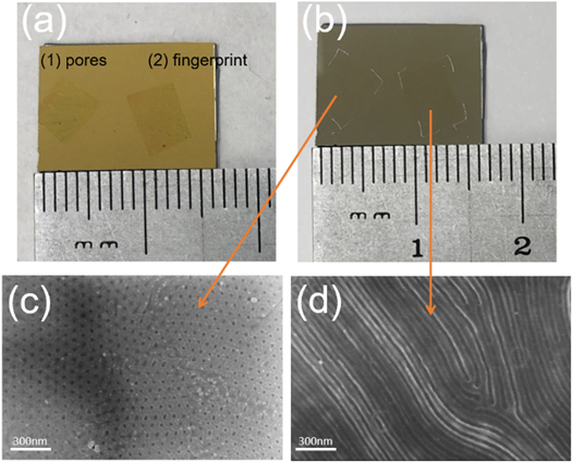
Figure 3. (a) rGO/BCP masks with (1) pores and (2) fingerprint patterns were both transferred onto the same SiNx substrate. (b) The sample was etched via CF4 RIE followed by oxygen plasma cleaning. (c) SEM image of pore patterns on the SiNx substrate. (d) SEM image of fingerprint patterns on the SiNx substrate. The above approach enables selective patterning of specific regions of a substrate where conventional spin-casting method may not be applicable or feasible.
Download figure:
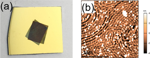
Standard image High-resolution imageTo further examine the applicability of the process, we applied our method to a number of polymer substrates. Polyethylene (PE) and polystyrene (PS) are prototypical flexible, inert plastics. The BCP mask was successfully relaminated onto PE with the phase separation as shown in figure 4(a). The sample was then soaked in ethanol for 30 min to form pores (figure 4(b)), after which the BCP mask can be used for surface modification of PE with a dry etching process. Notably, we extended our approach to PS substrates. Both the PS and the BCP used here (PS-b-P2VP) are soluble in toluene, which makes simple application and phase separation of BCP on PS impossible. However, interposing the RGO layer enables integration of PS and nanopatterned BCP. Figure 4(c) shows relaminated BCP/RGO mask on 35 mm cell culture PS petri dish. The mask is phase-separated in a fingerprint structure (figure 4(d)) and ready for dry etching.
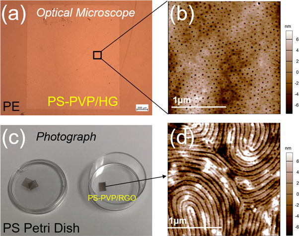
Figure 4. Transfer onto polymer substrates. (a) Optical micrograph of BCP/SLHG on PE. The lighter colored square in the center of the image is the PS-b-P2VP/HG mask. (b) AFM height image of open pore structure of the BCP mask on PE. (c) Photograph of BCP/RGO masks on 35-mm PS cell culture petri dish. (d) AFM height image of open fingerprint structure of the BCP mask on PS.
Download figure:
Standard image High-resolution imageSingle-layer HG is only one atomic layer thick; therefore, any holes or tears in the SLHG expose the substrate underneath the graphene layer. Thus, wafer-scale delamination and relamination of phase-separated BCP (PS-b-P2VP) is infeasible with SLHG as a transfer layer since the polymer tends to adhere strongly to the exposed substrate through imperfections in the SLHG layer. This adhesion tends to cause substantial damage to the SLHG/BCP stack when delamination on water is attempted, as the BCP adhered to the substrate sticks and causes more tearing in the overlayers. To circumvent this issue, we employed spin-coated or dropcast films of reduced graphene oxide (RGO) as the transfer layer (thickness ∼10–100 nm). These films, while still thin, are thicker than SLHG and cover the substrate more completely, obviating the adhesion problem and enabling more robust transfer of BCP films greater than several inches across. We and others have shown elsewhere that dropcast RGO films can enable water-based delamination of sheets on the order of 1 ft2 (∼600 cm2) with or without etchants [24, 30]. Importantly, another significant advantage over SLHG is that BCP masks can be delaminated after the open pores have been collapsed; therefore, additional ethanol soak and oxygen plasma etch processing steps after the mask has been moved to the target substrate are not necessary. In other words, all processes to generate BCP masks could be completed on the initial RGO-coated substrate, and once relaminated onto a new substrate, the mask will be immediately accessible for subsequent post-processing.
To illustrate the utility of RGO in large-area BCP lithography applications, we deposited GO across a 2-inch Si wafer and thermally annealed (in air at 250 °C for 30 s) to form mildly reduced GO, which is weakly adherent to its substrate [24]. We then spin-coated PS-b-P2VP onto the RGO film and phase separated the material using THF solvent annealing before transferring via delamination/relamination as previously described for SLHG above. Figure 5(a) shows the delamination of the entire 2-inch area of the open-pore PS-b-P2VP/RGO mask from SiOx and relamination onto another wafer with minimal damage to the membrane. We tested two different phase separation conditions by varying the solvent annealing time. We obtained pores (figure 5(b)) annealed for 5–10 min and parallel cylinder structures (figure 5(c)) annealed for 45 min and successfully transferred the phase-separated BCP masks onto new large wafers. Therefore, this approach is applicable to wafer-scale surface modifications.
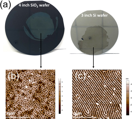
Figure 5. Wafer-scale transfer of PS-b-P2VP BCP mask using RGO as a transfer layer. (a) PS-b-P2VP/RGO on 4-inch SiO2 wafer and 3-inch Si wafer. AFM height images of: (b) PS-b-P2VP/RGO on SiO2, solvent annealed for 10 min to form an open pore structure, and (c) PS-b-P2VP/RGO on Si, solvent annealed for 60 min to form a parallel cylinder structure.
Download figure:
Standard image High-resolution imageAs a final demonstration, we highlight that this approach can modify surfaces with complex patterns by overlaying multiple PS-b-P2VP/RGO masks. Figure 6(a) shows an image of two PS-b-P2VP/RGO layers sequentially phase separated, delaminated and stacked onto a SiN substrate. Each layer was phase separated with fingerprint structures before transfer to SiN, the second layer being relaminated onto a dried first layer. Figure 6(b) shows an AFM image of the etched SiN surface after CF4 RIE for 2 min and subsequent cleaning with oxygen plasma for 5 min. The resulting overlapped fingerprint grooves—in two different fingerprint patterns—is apparent from the image. The appearance of amorphous residues in figure 6(b) is likely due to contaminants which are trapped between the two BCP/RGO layers during transfer. With delamination and relamination in an ultraclean environment, these residues might be less prominent. This result suggests that emergent complexity could be generated through overlapping lattices (e.g., moiré structures) by rationally designing multiple BCP/RGO layers. RGO is robust and can be tailored in any size and shape, as shown in figure 5, to modify surfaces with special patterns. Although the current result in figure 6 is from a non-oriented fingerprint BCP mask, potentially multiple layers of pre-defined masks can be developed by using our approach.
Figure 6. (a) Optical image of two sequentially transferred and stacked PS-b-P2VP/RGO masks onto SiNx substrate. (b) AFM image taken after CF4 RIE for 2 min and subsequent surface cleaning with oxygen plasma for 5 min, two different directions (horizontal and vertical) of fingerprint patterns were etched on SiNx substrate.
Download figure:
Standard image High-resolution image
4. Conclusion
We demonstrated the use of single-layer hydrogenated graphene or reduced graphene oxide (RGO) as thin support layers for phase-separated block copolymer (BCPs) and for nanoscale pattern transfer. We use weakly-bound graphene-based films to delaminate subsequent adlayers via a simple water lift-off. The mildness of the transfer technique allows phase-separated BCPs to be deposited on almost any substrate without concerns about contamination from harsh chemical etchants. We have shown the utility of this technique for employing phase-separated BCPs as lithographic masks for the substrates SiN and polyethylene, and we have shown that this technique enables transfer of BCP patterns to polystyrene, a result that is impossible without an interposing graphene layer. We also demonstrated that thin layers of RGO can be employed in wafer-scale BCP lithography on Si and SiOx. Finally, we have shown that we can achieve complex hierarchical patterns by stacking multiple BCP mask layers, a technique that cannot be performed using standard BCP phase separation on a single substrate. Future development of this process will focus on thin-film techniques that are more adaptable to large areas, such as doctor blading. These techniques enable lithography of regular nanoscale patterns over large areas, and may find application in nanofiltration membranes, antireflective coatings, and photonically active materials.
Acknowledgments
This work was funded by the Office of Naval Research through Base programs at NRL.
Data availability statement
The data that support the findings of this study are available upon reasonable request from the authors.