
Characterization of Soldering Alloy Type Bi-Ag-Ti and the Study of Ultrasonic Soldering of Silicon and Copper


1
Faculty of Materials Science and Technology in Trnava, Slovak University of Technology in Bratislava, Jana Bottu No. 2781/25, 917 24 Trnava, Slovakia
2
FMT—Faculty of Materials Science and Technology, Technical University of Ostrava, 17. Listopadu 15, 708 33 Ostrava-Poruba, Czech Republic
*
Author to whom correspondence should be addressed.
Metals 2021, 11(4), 624; https://doi.org/10.3390/met11040624
Submission received: 16 March 2021
/
Revised: 6 April 2021
/
Accepted: 8 April 2021
/
Published: 13 April 2021
Abstract
:The aim of the research work was to characterize the soldering alloy type Bi-Ag-Ti and to study the direct soldering of silicon and copper. Bi11Ag1.5Ti solder has a broad melting interval. Its scope depends mainly on the content of silver and titanium. The solder begins to melt at the temperature of 262.5 °C and full melting is completed at 405 °C. The solder microstructure consists of a bismuth matrix with local eutectics. The silver crystals and titanium phases as BiTi2 and Bi9Ti8 are segregated in the matrix. The average tensile strength of the solder varies around 42 MPa. The bond with silicon is formed due to interaction of active titanium with the silicon surface at the formation of a reaction layer, composed of a new product, TiSi2. In the boundary of the Cu/solder an interaction between the liquid bismuth solder and the copper substrate occurs, supported by the eutectic reaction. The mutual solubility between the liquid bismuth solder is very limited, on both the Bi and the Cu side. The average shear strength in the case of a combined joint of Si/Cu fabricated with Bi11Ag1.5Ti solder is 43 MPa.
1. Introduction
The technological progress in the field of heavy-duty electronics is ever more oriented to the production of equipment operating permanently at much higher temperatures. The present serviceability demands in the field of heavy-duty electronics are defined in some parts of devices even at the level of service temperatures up to 225–350 °C [1]. The requirements are directed mainly to ensuring the life of equipment at such high temperatures in different service situations. This is, for example, the case of measurements carried out during drilling work or during crude oil and natural gas recovery, geo-thermal measurements, sensors for pressure control, control of modern powerful engines, production of hybrid micro-circuits, and hybrid electronic modules for the space industry, etc.
In the production of such sensitive devices, one must follow from the most recent knowledge, and the scientific institutions in the world present different solutions for joining different materials such as welding, combination of friction drilling and form tapping, brazing, or in this case, soldering [2]. The issue of the development of suitable soldering alloys for power electronic equipment differs according to the kind and purpose of application. In some cases, it is necessary for the soldering alloy to have a relatively low melting point. Such solders are used in the case of the so-called gradual soldering, where during assembly of the packaged part some of the solder must have a lower melting point than the others. This solution is necessary to avoid damaging already soldered joints in a combined part [3]. For the production of such a part, solders based on Sn-Cu, Sn-In, Sn-Sb, Sn-Bi, or Bi-Sn are used [4,5,6].
Another case consists of designing a soldering alloy that is able to resist higher application temperatures in a part. The solders suitable for higher application temperatures should have melting points within the range of approximately 260–420 °C. For this condition suitable solders are those based on Zn, Sn, Au, or Bi with a properly selected combination of alloying elements [7,8,9,10,11].
An important factor in the production of heavy-duty electronic modules is the fact that the packaged module consists of different mutually connected materials. The core of such a part consists of semiconductor matrixes, which are joined with metallic, non-metallic, ceramic, or composite materials. The connecting material for the integrated electronic part is the solder. An issue in soldering dissimilar materials is in the wetting, or possible non-wetting, by commercial solders. The wettability issue of semiconductor materials can be solved by their coating and subsequent soldering. The deposited coating will ensure the surface wetting [12]. In such a case it is possible to use commercial solders for higher application temperatures. However, nowadays the so-called direct soldering technology is gaining more popularity. Direct soldering allows mutually different materials to be soldered without any interlayers, which brings considerable savings of the financial means for the technologies and the coating materials required. The solution consists in suitable alloying of soldering alloys by the active elements. The alloys containing these elements possess a higher affinity to one or more elements of the semiconductor or ceramic substrates and, with the application of a proper soldering technology, are then capable of joining their surfaces. The most frequently used element added to solders is titanium, but other active metals are also used. The efficiency of solders alloyed with titanium is documented in the scientific works of many authors [13,14,15,16,17,18,19]. Xian [12] studied the wettability of Si-Al-O-N ceramics and copper by Sn-Ti based solders with the addition of Cu, Ni, Ag, In, or Al during vacuum soldering at temperatures varying from 427–827 °C. He found that the solders have very low wettability at temperatures below 727 °C. Other elements added to Sn-Ti solder affected mainly the wetting of Cu substrate. Qu et al. [20] studied the effect of Ti or Y in Sn-Ag-Ti solder when soldering Cr-Ni-Ti alloy with copper. The bond on the Cr-Ni-Ti side of the substrate was formed owing to Ti reaction with the solder. The authors assume that Ti plays an important role in the formation of that bond. They attained an average shear strength of 45.3 MPa. In our previous work [21], we also carried out research on the soldering of AlN ceramics with Sn-Ag-Ti based solder. The effect of Ti in the joint boundary was clearly proved. New reaction products such as NTi and AlTi2 were identified in the boundary and had an unmistakable effect upon the formation of a sound joint. The average shear strength of the AlN/Sn-Ag-Ti/Cu joint was 29.5 MPa. Weber and Rettenmayr [22] used an active Bi-Ag based solder with the addition of Ti and Mg for soldering the combination of SiO2 and stainless-steel type 316 L. The joint was fabricated at the temperature of 780 °C in a shielding atmosphere of argon. In the solder/stainless steel boundary, a reaction layer of Fe-Ti-Bi was identified. With increasing Ti content, a more pronounced reaction in the boundary was observed. Reaction products rich in Ti were formed in the solder/SiO2 boundary.
In order that the solder alloyed with an active metal will wet the semiconductor material, it is necessary to activate it during soldering. Ti activation may be realised by heating at a high temperature (750–900 °C) or by ultrasound energy at the melting point of the solder. High temperature activation is impossible in most cases. Therefore, the soldering method with ultrasonic activation is preferred [23,24].
The effect of ultrasound on bond formation between the solder alloyed with Ti and a semiconductor or ceramic substrate is documented in several professional publications [25,26,27,28,29].
It was found that ultrasonic soldering with solders containing Ti ensured the wetting of ceramic or semiconductor substrates. It allows the formation of AlTi, Al2Ti, TiO2, TiC, or TiN compounds with the surface of these materials. The authors in their works have also proved the evident formation of a TiSi2 reaction layer between the Sn-Ag-Ti solder and silicon.
This work therefore deals with the study of soldering alloy type Bi-Ag-Ti and research of ultrasonic soldering of silicon and copper. The application of the solder type Bi-Ag-Ti is oriented for high to very high application temperatures. Titanium in solder was selected as an active metal for the wetting of the semiconductor Si substrate. The solder is alloyed with silver in order to improve the strength and electric conductivity. Thus, the research consists in the study of the solder proper and subsequently of the research of the interactions in the solder/substrate boundary after soldering by a hybrid method–hot plate/ultrasound.
2. Experimental
The manufacturing of soldering alloy consists of determining the weight proportions of the individual elements and their charging and manufacture in the as-cast condition in an induction vacuum oven. All the input components of the solder were in a high purity of 4N. The manufacture was performed in argon overpressure of 200 Mbar at a temperature around 1100 °C, when the Ti slowly dissolved in the solder. This resulted in an experimental alloy with the composition given in Table 1.
The chemical analysis of the alloy was performed by the method of atomic emission spectrometry with induction-coupled plasma (ICP-AES). The analysis of individual elements was realized on SPECTRO VISION EOP equipment (SPECTRO Analytical Instruments GmbH, Kleve, Germany). The samples of alloys for ICP-AES analysis were dissolved in suitable chemical solutions of acids and bases. The analysis proper was performed on an atomic emission spectrometer with a pneumatic atomizer and a Scott atomizing chamber.
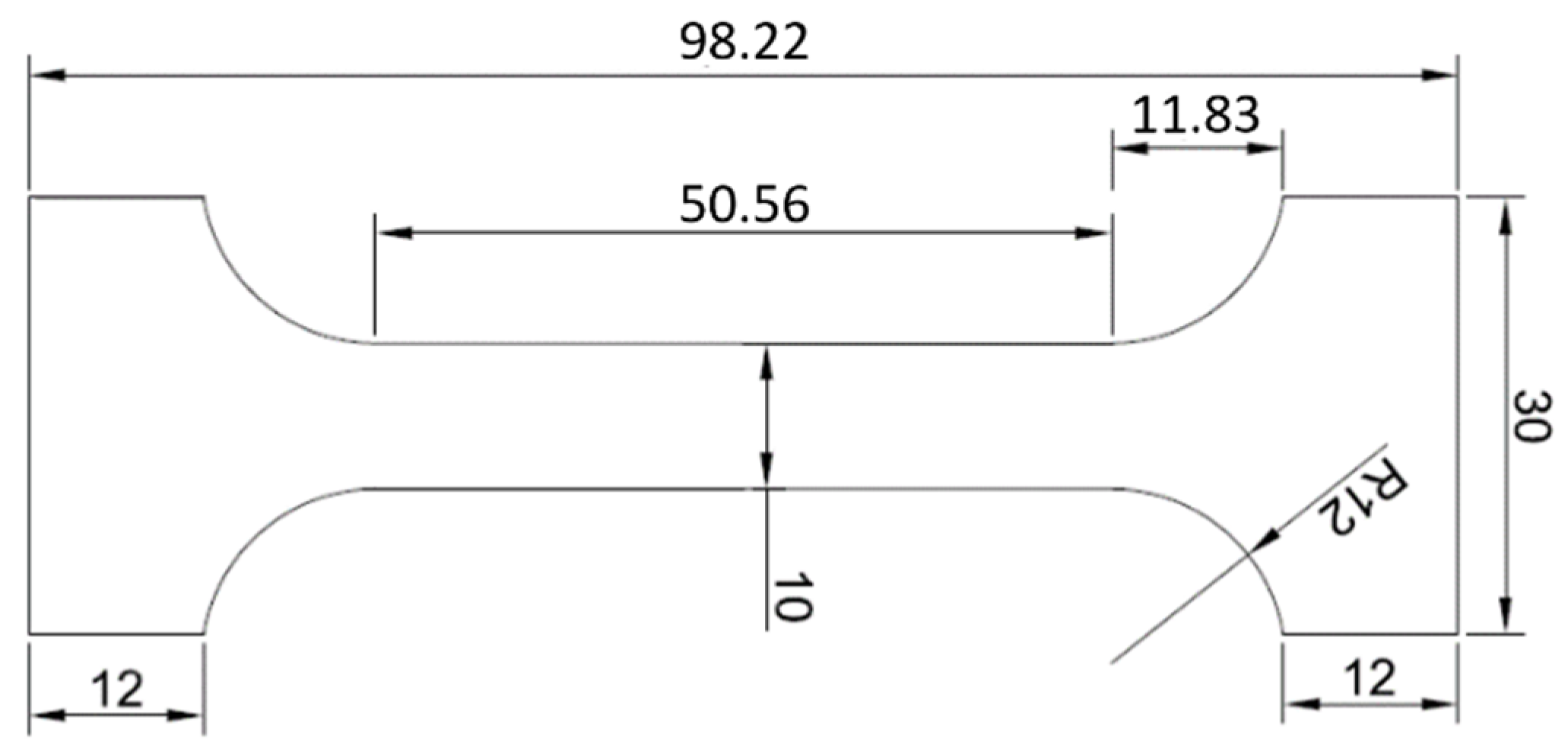
Six test pieces were machined for the tensile strength measurement of the solder, with dimensions as shown in Figure 1. All values are given in mm. The test piece thickness was 4 mm. The cross-section in the throat area was 40 mm2. The tensile strength was measured on a versatile tearing machine type LabTest 5.250SP1-VM (Labortech Ltd., Praque, Czech Republic). The tearing rate was 1 mm/min.
The following substrates were used for experimental soldering with Bi11Ag1.5Ti solder:
- Silicon substrate with dimensions Ø 15 × 6 mm2
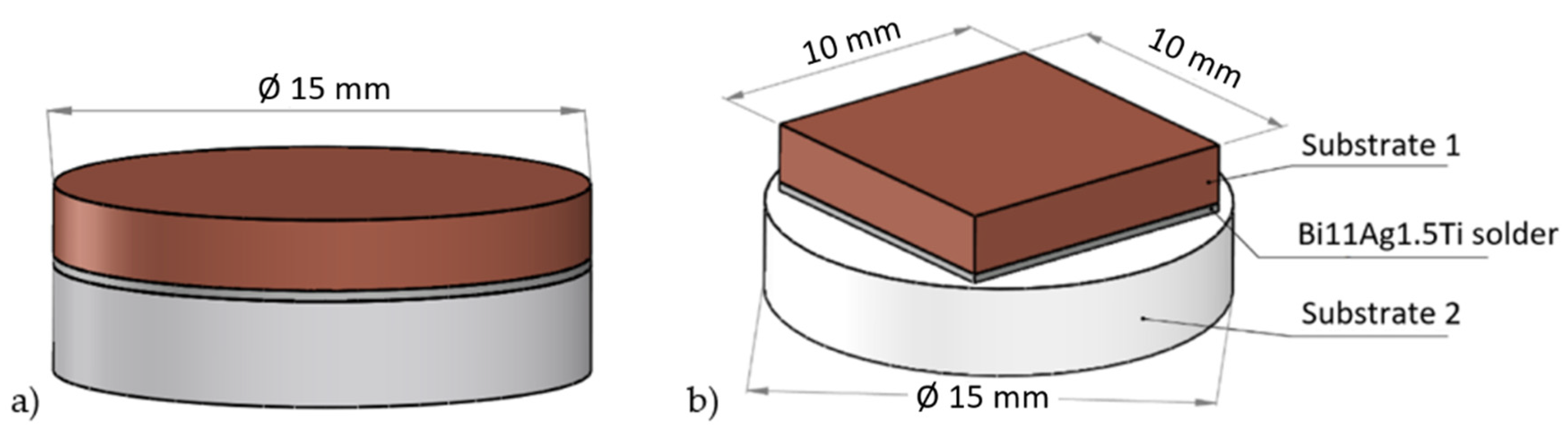
- Copper substrate with dimensions Ø 15 × 2 mm2 and 10 × 10 × 3 mm3
- Nickel substrate with dimensions 10 × 10 × 2.5 mm3
- Ceramic substrate Al2O3 with dimensions 10 × 10 × 3 mm3
- Ceramic substrate ZrO2 with dimensions 10 × 10 × 3 mm3
- Ceramic substrate Si3N4 with dimensions 10 × 10 × 3 mm3
- Ceramic substrate SiC with dimensions 10 × 10 × 3 mm3
The scheme of the soldered joint prepared for the chemical analysis of the solder/substrate boundaries and for the shear strength measurement is shown in Figure 2.
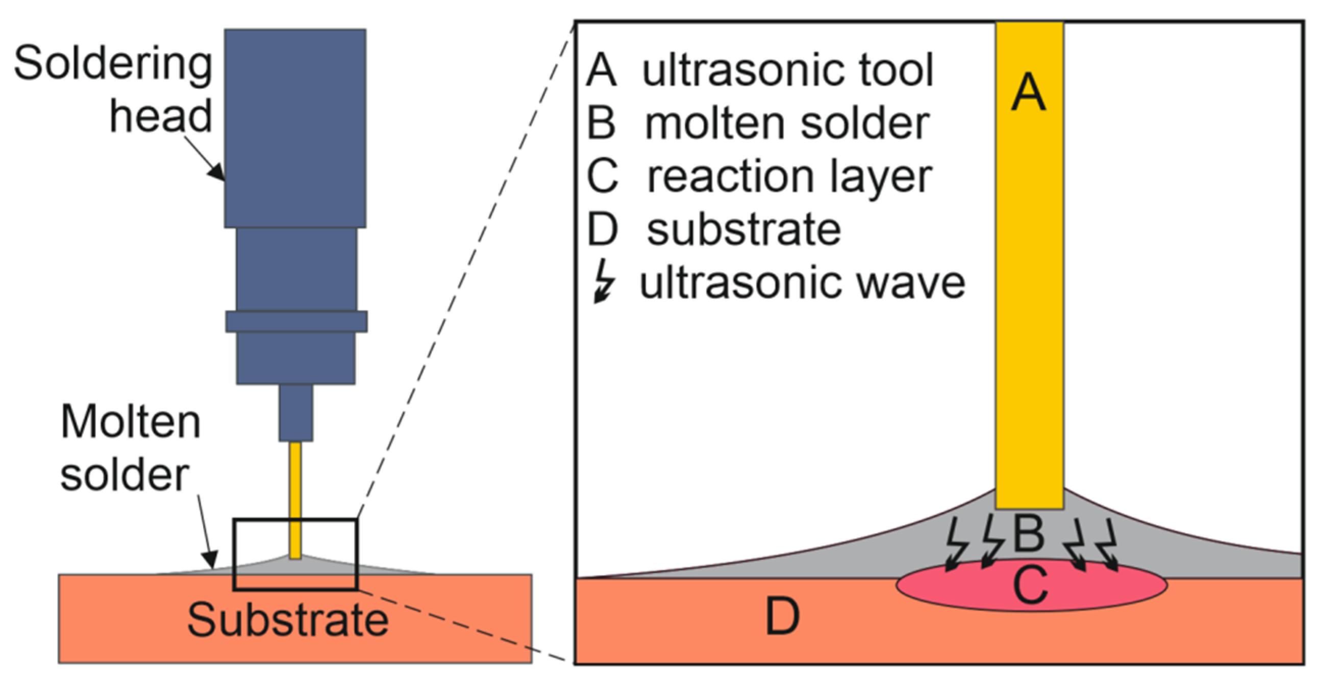
The joints were fabricated by a hybrid soldering method—hot plate/ultrasound. The soldering temperature was adjusted by the thermostatic control on the heating element. The substrate of each material was laid on the hot plate and the solder was laid on it. The arranged materials were heated at the soldering temperature. After the solder had melted on the surface of the substrates, ultrasonic power was supplied to the molten solder. For ultrasonic power generation, the equipment type HANUZ UT2 (HANUZ s.r.o. Nove Mesto nad Vahom, Slovakia) was applied. The transfer of ultrasonic power to the molten solder was ensured by an encapsulated ultrasonic transducer with a piezo-electric oscillation system and a titanium sonotrode with the end tip diameter of Ø 3 mm. The schematic representation of the application of ultrasonic vibrations to the molten solder is shown in Figure 3. The temperature during soldering was continually monitored using a NiCr/NiSi thermocouple. Owing to the presence of ultrasound and its cavitation and cleaning effect, the redundant solder was removed and the individual couples of substrates were laid on each other from the side of the molten solder and the joint was thus formed. The soldering parameters are given in Table 2.
The machined specimens were prepared by standard metallographic procedures of grinding, polishing and etching for accentuation of the microstructure. This concerned mainly the accentuation of the transition zone in the solder/substrate boundary. Grinding was performed on SiC grinding disks with the granularity of 320, 600, and 1200 grains/cm2. Polishing was performed using a diamond emulsion with the diamond particle sizes of 9 μm, 6 μm, 3 μm, and 1 μm. The final polishing was done using emulsion type OP-S (Struers) with the grain size of 0.2 μm.
The analysis of the solder microstructure was performed by electron scanning microscopy (SEM) on the equipment type TESCAN VEGA 3 (Tescan Orsay Holding, Brno, Czech Republic). The qualitative and semi-quantitative chemical analysis of the solder and joint boundaries was carried out on the equipment type JOEL 7600 F (JOEL Ltd., Tokyo, Japan) with an X-ray micro-analyzer type Microspec WDX-3PC (Microspec Ltd., Peterborough, NH, USA).
The phase composition of the soldering alloy was identified by the X-ray diffraction analysis on specimens with dimensions of 10 × 10 mm2. The equipment type PANalytical X´Pert PRO (Malvern Panalytical Ltd., Malvern, UK) was used. Step size parameter was 0.013° and scan step time parameter was 29.07 s.
The TG/DTA analysis of the Bi11Ag1.5Ti solder was performed on the equipment type DTA SETARAM Setsys 18TM (NETZSCH-Gerätebau GmbH, Selb, Germany). The measuring system is provided with a cylindrical oven with a graphite heating element and appropriate control thermocouple, measuring rod and the cooling medium. The crucibles (Al2O3) with inserted measured and reference specimens were laid free on the measuring rod during the experiment and were in contact with two thermocouples serving to measure the difference in temperature between the measured and reference specimen. The heating rate of the specimen was 5 °C/min from room temperature up to the temperature of full melting of the specimen. This enabled the definition of the temperatures of phase transformations in the liquidus-solidus range and in the solid state, and the enthalpies of the phase transformations were also determined.
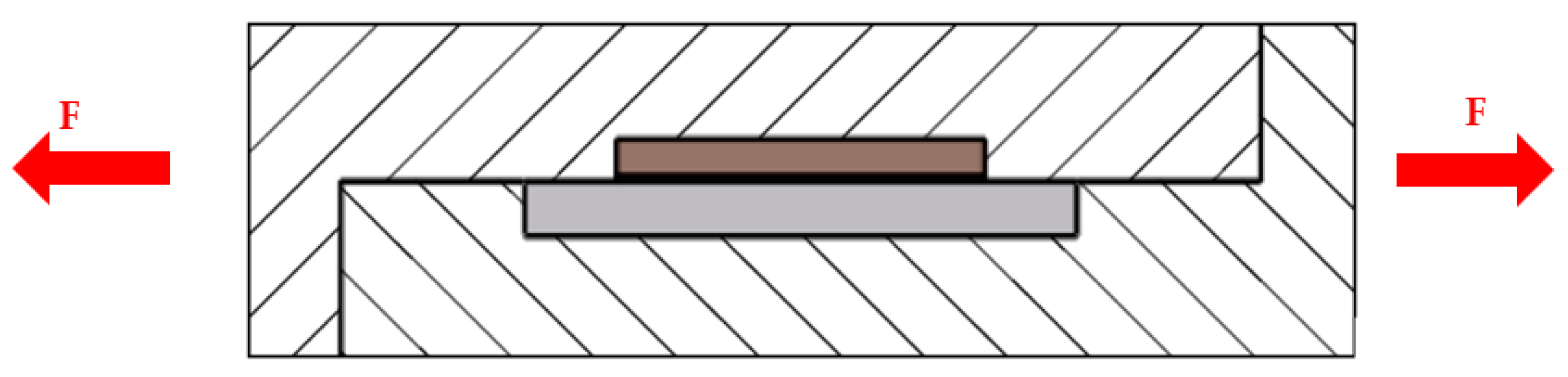
Due to the different coefficients of thermal expansivity of the materials used, the soldered joints, during the service of equipment, are loaded mainly in shear. For that reason, measurements of the shear strength were performed using the equipment type 5.250SP1-VM. A special jig for spacing the specimens in order to ensure uniform shear loading was employed in these measurements. The schematic representation of the measurement layout is shown in Figure 4.
3. Experimental Results
3.1. TG/DTA Analysis
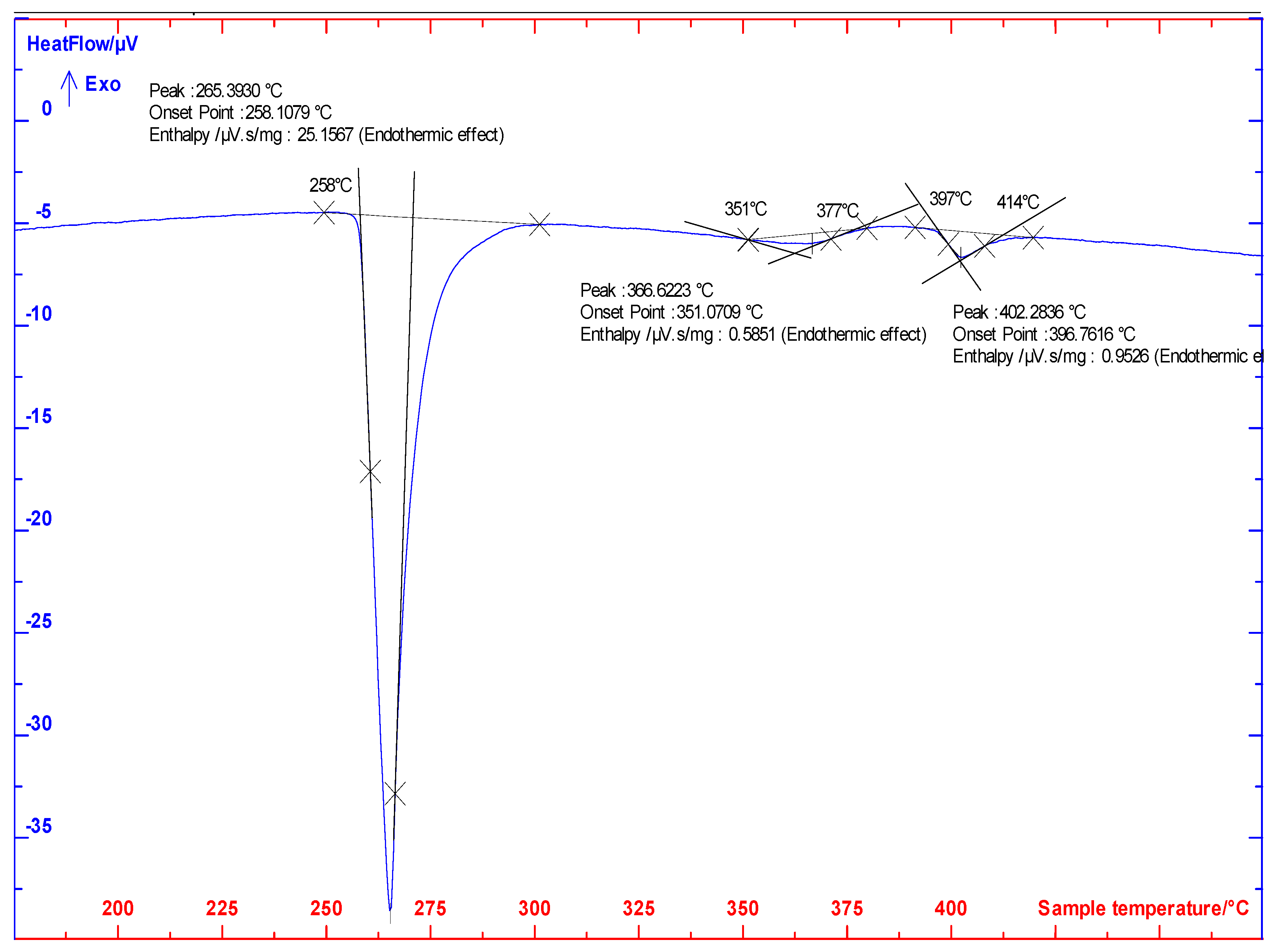
The TG/DTA (Differential Thermal Analysis/ Thermogravimetry) analysis was always performed twice at the heating and cooling rate of 5 °C/min (Figure 5).
Significant temperatures of the three phase transformations in soldering alloy type Bi11Ag1.5Ti determined by the TG/DTA analysis are documented in Table 3.
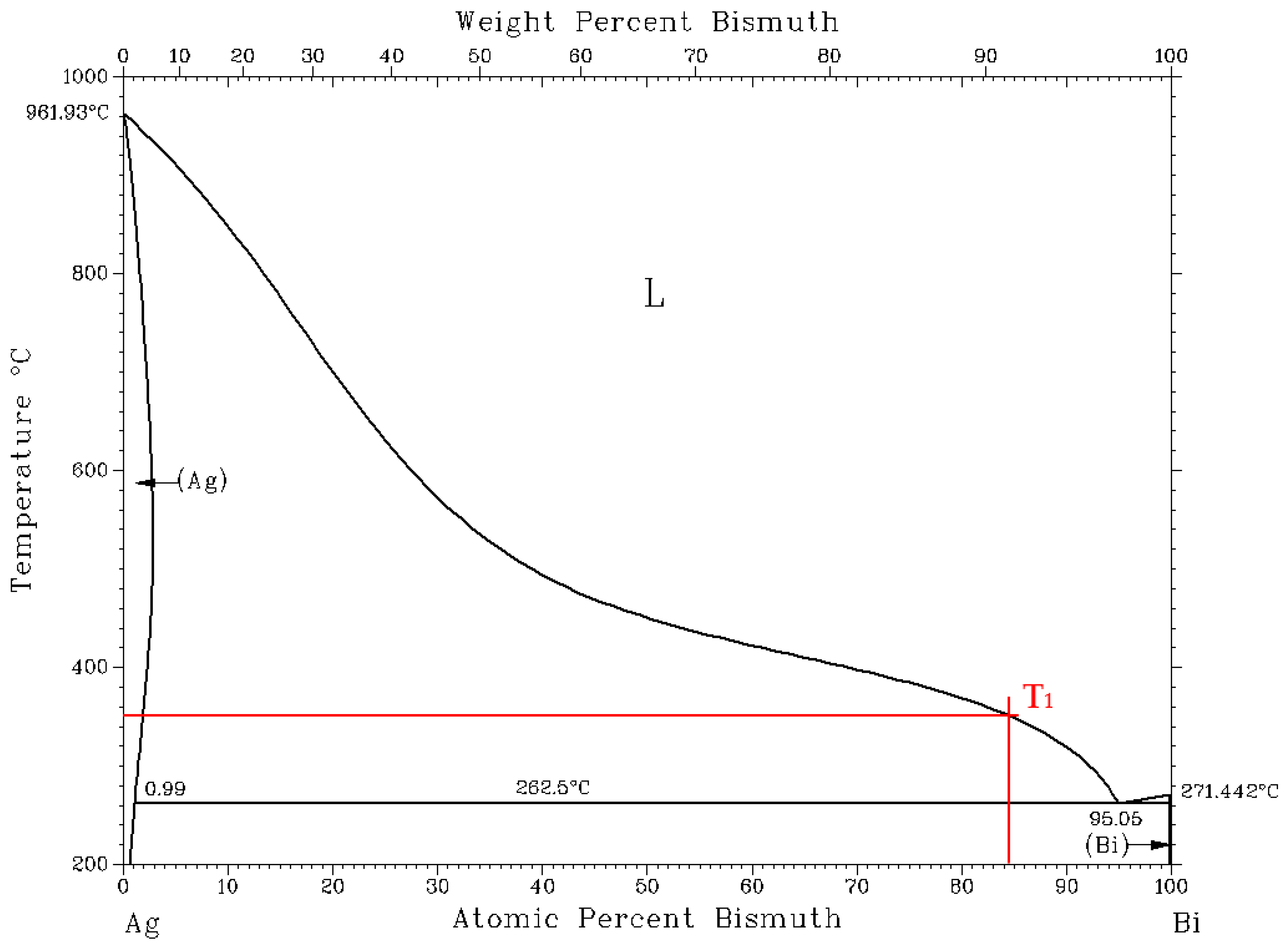
Three distinct peaks may be observed in the TG/DTA record. The highest peak corresponds to the eutectic reaction. The Bi–Ag system is of the eutectic type (Figure 6) with the eutectic reaction temperature of 262.5 °C, and the eutectic point on the bismuth side is 95.05 at.% Bi. The maximum solubility of Bi in Ag at this temperature is 0.99 at.% Bi. On the other hand, the solubility of Ag in Bi is negligible.
From Figure 5 it is obvious that the Bi11Ag1.5Ti solder is not of eutectic composition, since it has a broader melting interval.
From the results of the TG DTA analysis the following conclusions follow:
At the temperature from 401–405 °C the Bi11Ag1.5Ti alloy precedes the liquidus temperature (TL). In the next stage (T1), at 355 °C, silver starts to precipitate with approximately 2 at.% Bi. The last stage (TE) represents the following eutectic reaction:
L = (Ag) + (Bi)
3.2. Microstructure of Bi11Ag1.5Ti Solder
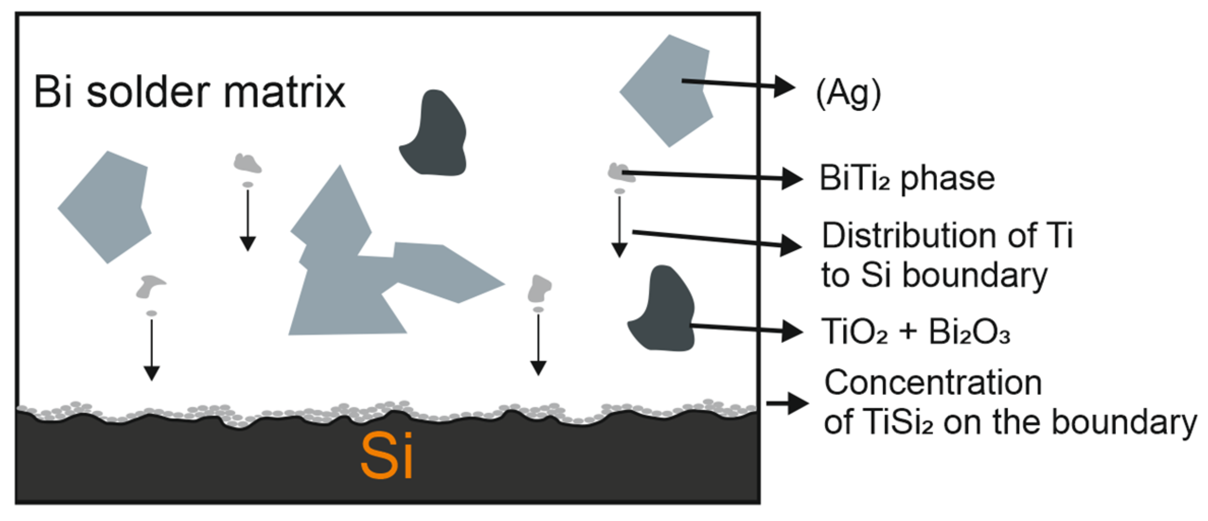
The microstructure of the soldering alloy type Bi11Ag1.5Ti consists of bismuth matrix. The solder matrix contains crystals of solid solution of silver (Ag) and intermetallic phases of titanium. The microstructure, with designation of the phases, is documented in Figure 7.
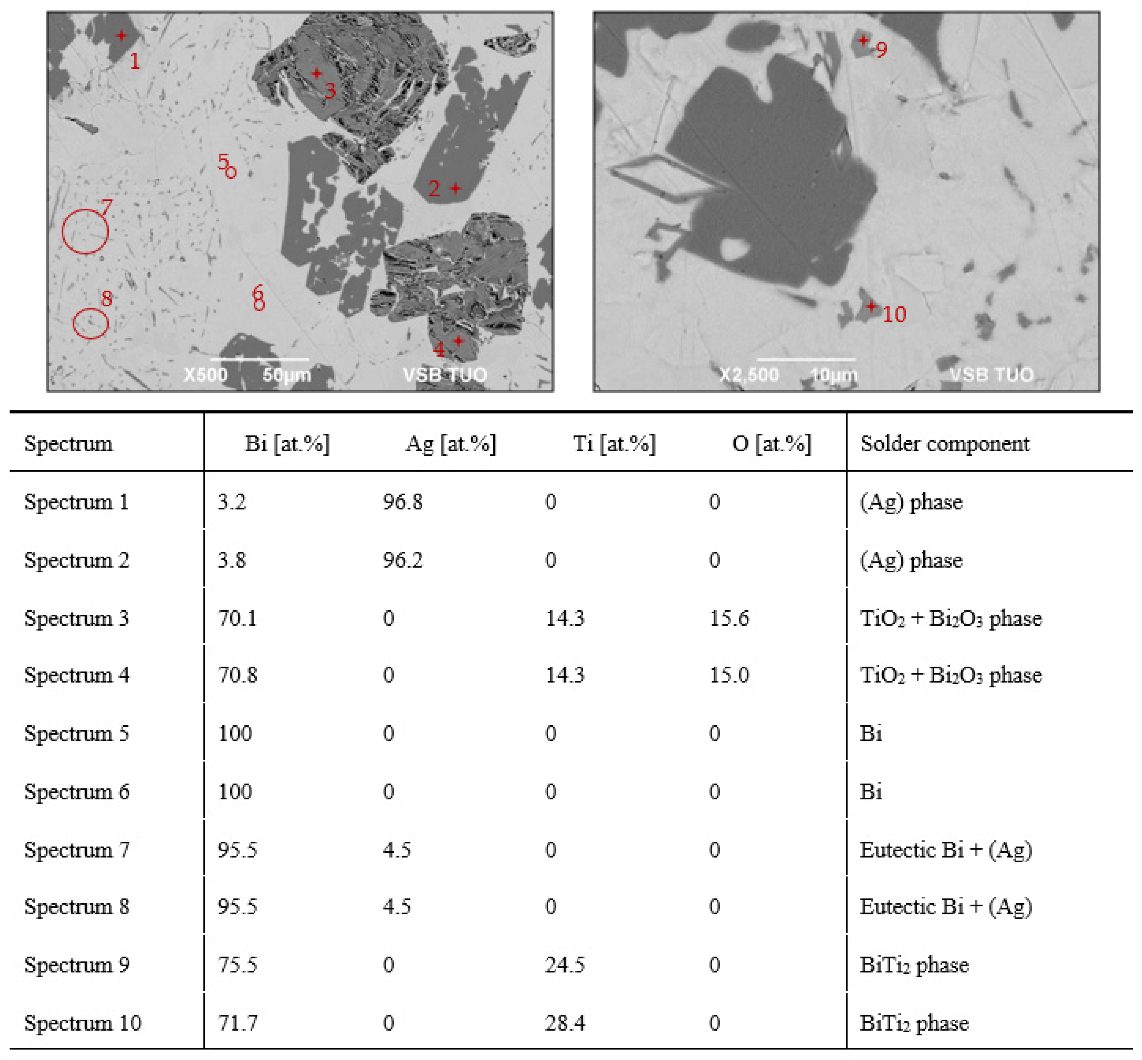
For determination of the chemical composition in the individual components of the soldering alloy, EDX (Energy Dispersive X-ray) analysis was performed. The points of measurement are shown in Figure 8 and are marked with numbers from 1–10.
The measuring points of Spectrum 1 and 2 are composed of solid solution of silver (Ag) containing below 2 at.% Bi. At the measuring points of Spectrums 3 and 4 there are relatively large areas of oxide phases-TiO2 + Bi2O3. Segregation of Ti2Bi has occurred primarily, even at higher temperatures, whereby some of the titanium and bismuth has managed to oxidize. The measuring points of Spectrum 5 and 6 represent the zone of pure bismuth. A zone with the occurrence of Bi + (Ag) eutectics was observed at the measuring points of Spectrums 7 and 8. Silver occurred in eutectics in the form of lamellas non-uniformly dissipated in pure bismuth. Locations where Ti2Bi phase occurred were identified in the measuring points of Spectrum 9 and 10. The most recent binary diagram of the Bi–Ti system is mentioned by Okamoto [31], where the existence of several intermetallic phases of type BixTiy is obvious.
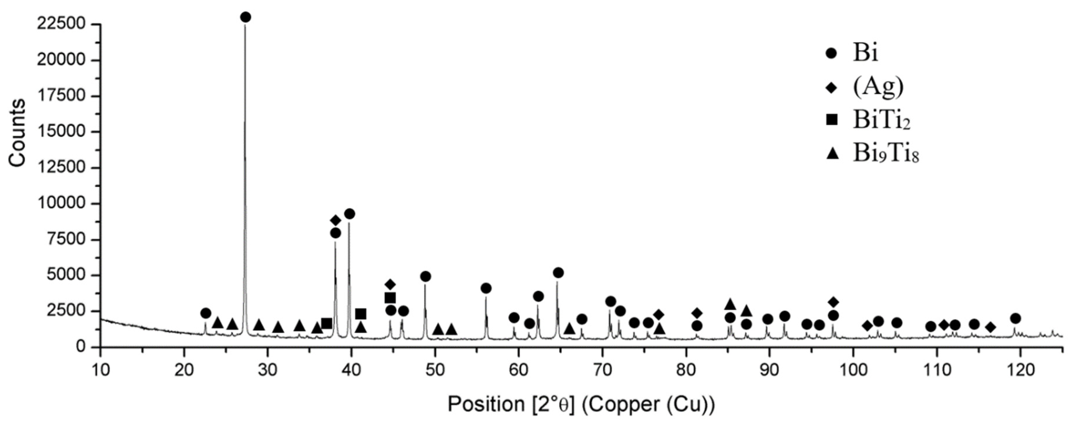
The diffraction XRD analysis of Bi11Ag1.5Ti solder proved the presence of bismuth (Bi), solid solution of silver (Ag), and intermetallic phases of bismuth and titanium; BiTi2 and Bi9Ti8 were revealed by the binary diagram Bi-Ti [31]. The presence of BiTi2 intermetallic phase in the solder matrix was proved also by the EDX analysis. The record from the diffraction analysis is documented in Figure 9.
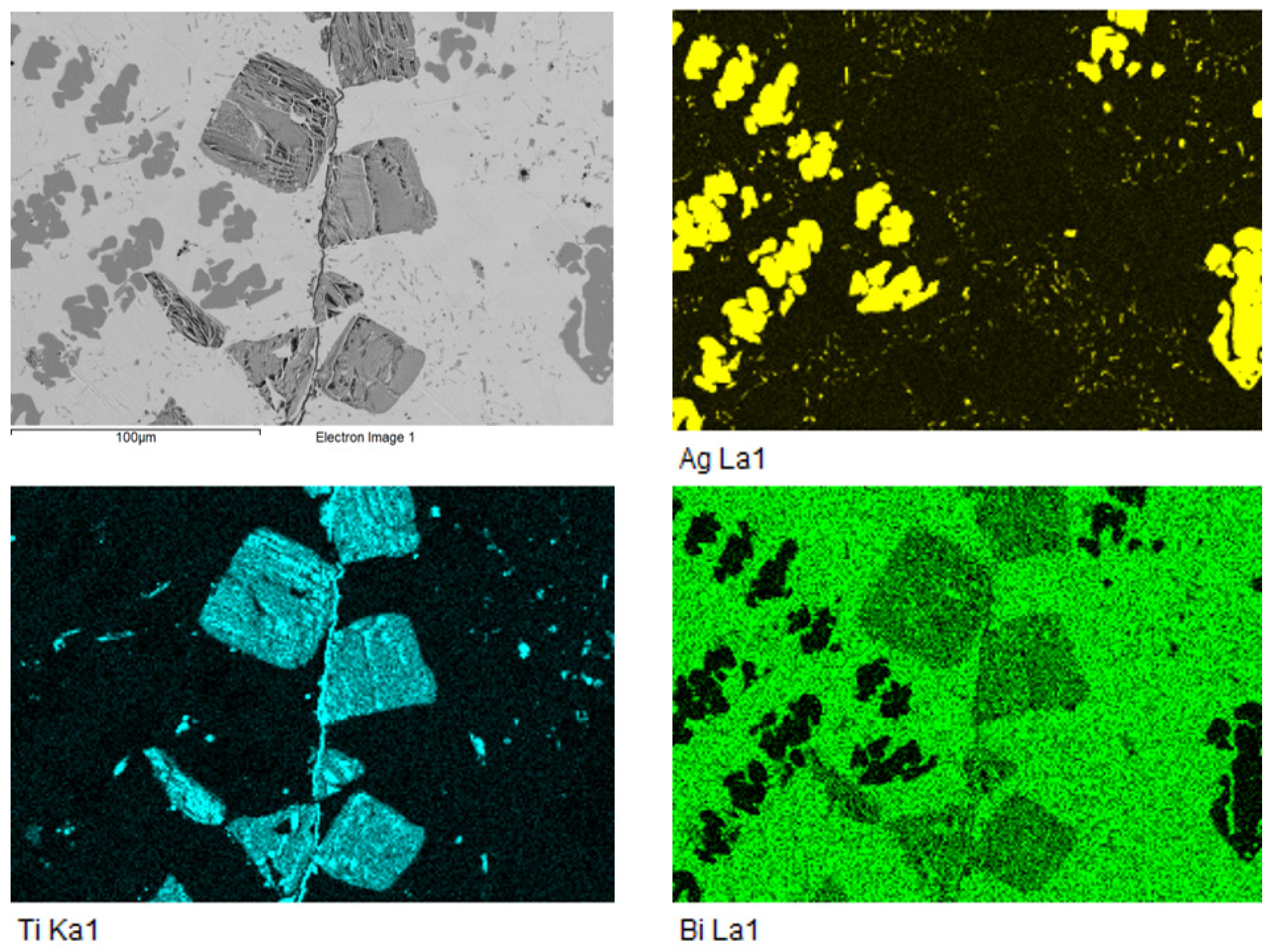
The planar distribution of silver crystals and the intermetallic phase of titanium and bismuth in the matrix is documented in Figure 10.
3.3. Tensile Strength of Soldering Alloy
The mechanical test was oriented to determine the tensile strength of the active soldering alloy type Bi11Ag1.5Ti. The shape and dimensions of the test pieces were designed and calculated. Six specimens were used for the measurement of the tensile strength in the experimental solder. The loading rate of each specimen was 1 mm/min.
The specimens provided values with a low scatter in tensile strength. The highest measured tensile strength of Bi11Ag1.5Ti solder was 43 MPa. The lowest measured strength was 41 MPa. The average tensile strength calculated from the measured values was 42 MPa.
3.4. Microstructure of Si/Bi11Ag1.5Ti/Cu Joint
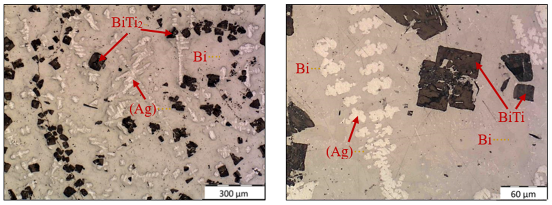
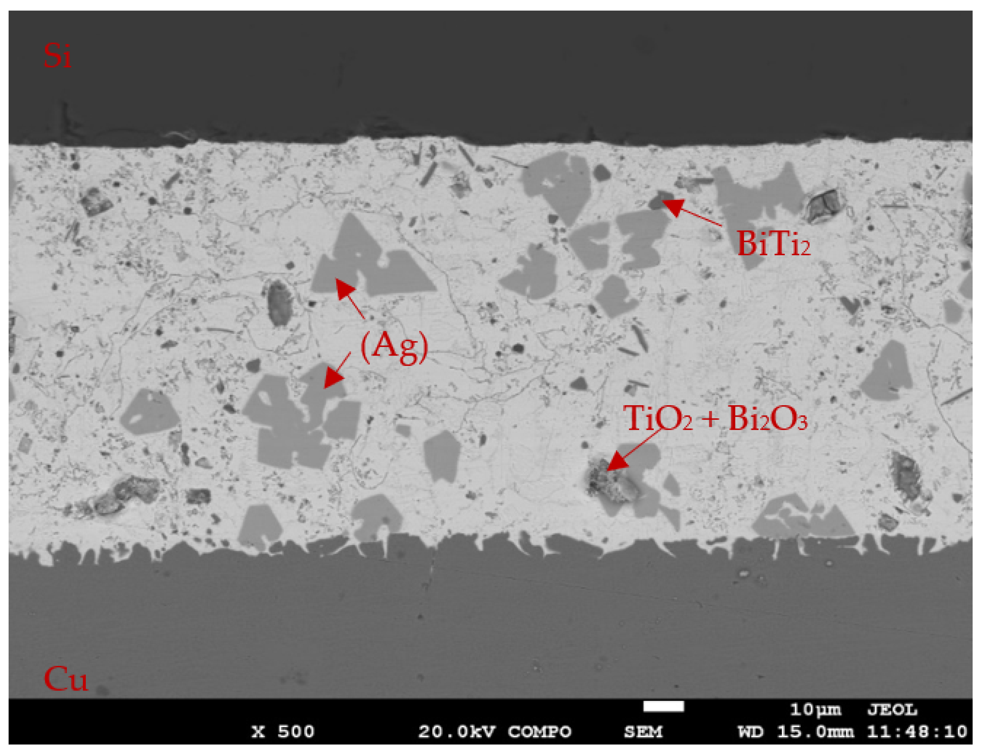
The soldered joint of Si/Bi11Ag1.5Ti/Cu was fabricated at the temperature of 380 °C. An acceptable joint was obtained by ultrasound activation, which did not contain any cracks or imperfections. The microstructure of the soldered joint is shown in Figure 11.
Figure 11 shows that large particles of silver phases and smaller particles of titanium phases occur in the solder matrix after soldering. An undulating boundary was formed in the Cu/solder boundary, representing the eutectic bond between bismuth and copper. This reaction is significantly supported by the power ultrasound.
3.5. Analysis of Transition Zone in Si/Bi11Ag1.5Ti Joint
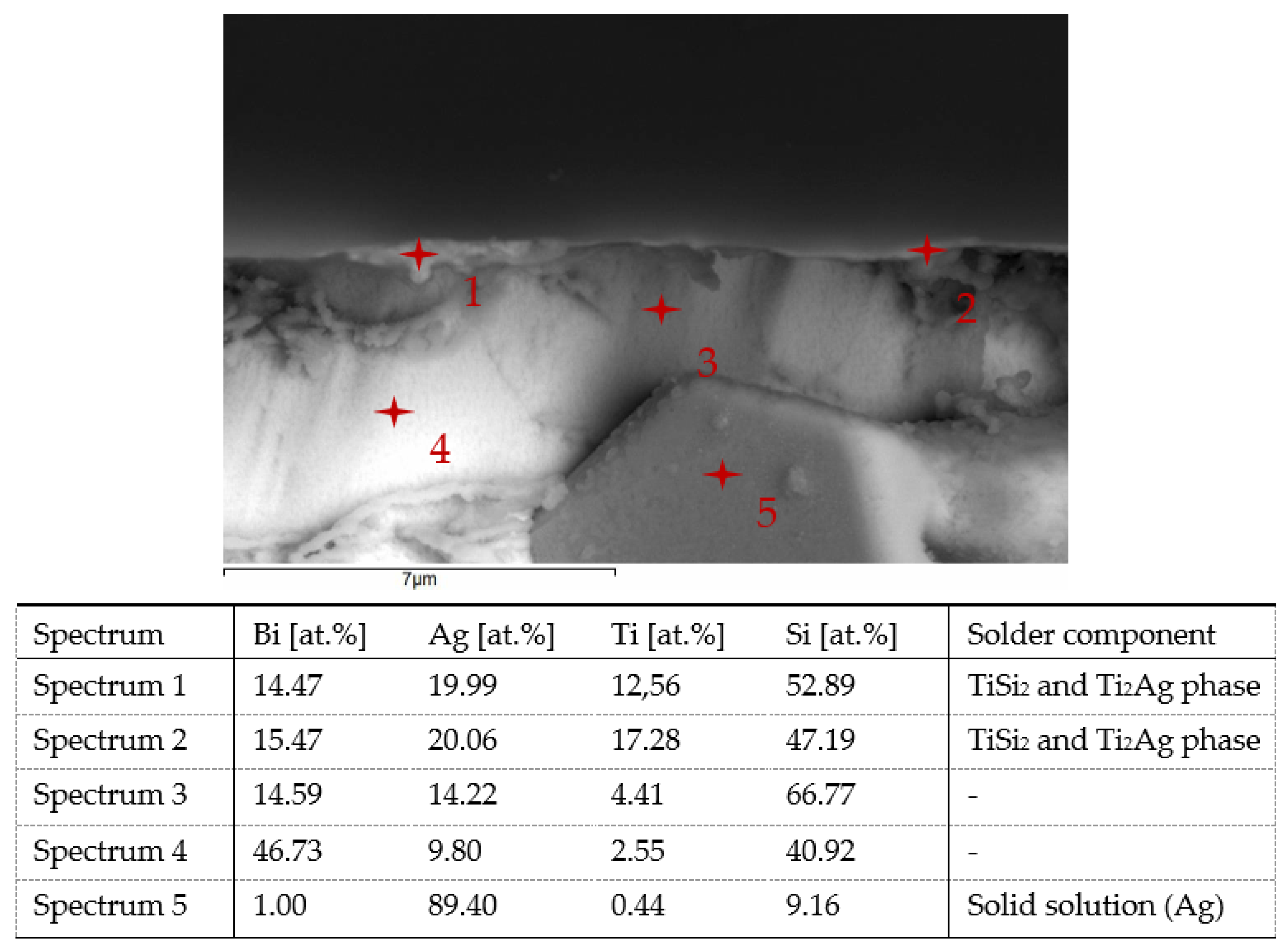
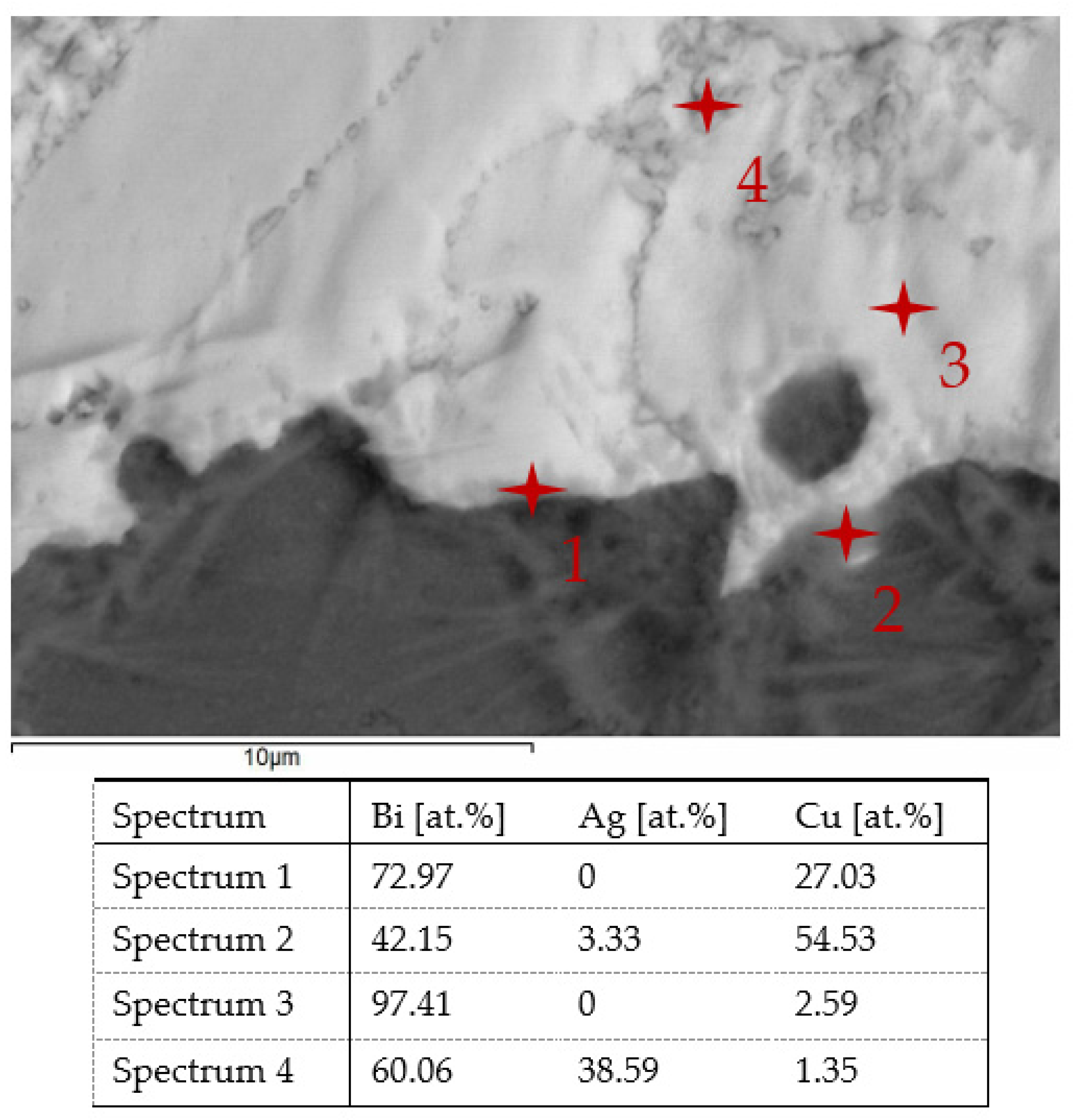
In order to determine the chemical composition and to identify the individual phases, EDX analysis of the soldered joint was performed (Figure 12).
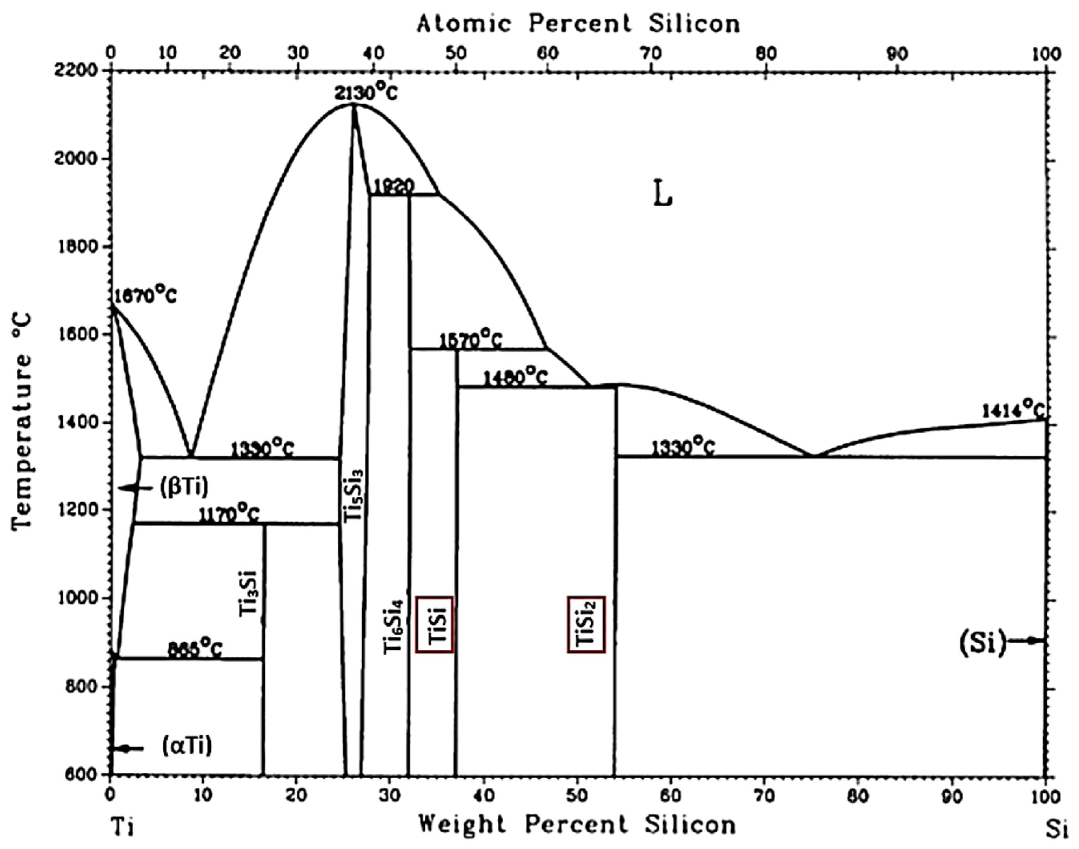
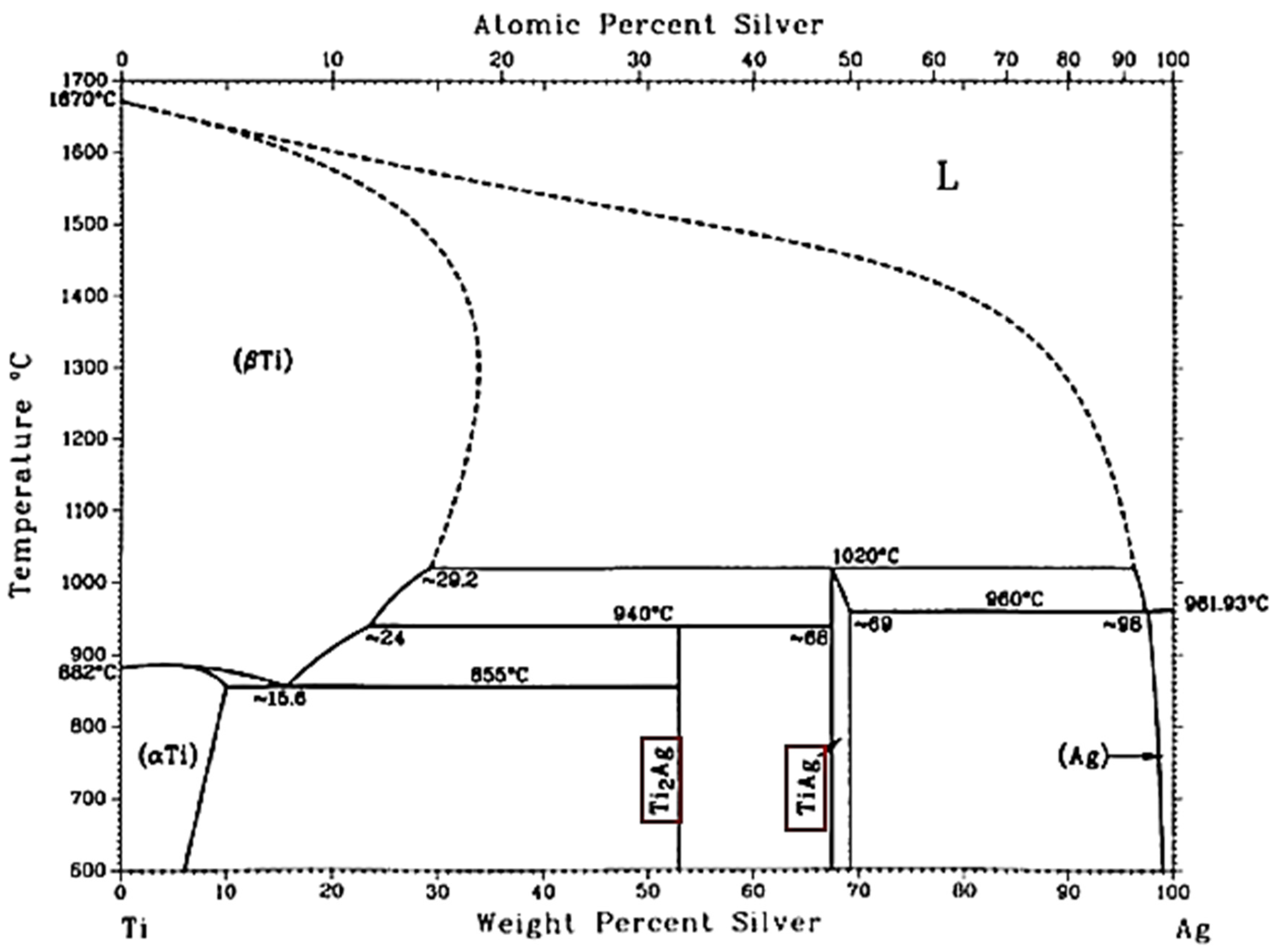
Measurement was performed at 5 points-Spectrum 1–5 (see Figure 12). The points of measurements 1 and 2 were situated directly on the Si/solder boundary. High Si content from the substrate was observed, while the Bi content was at the level of 3 at.%. The high titanium and silver content proves the interaction with silicon at the formation of probable TiSi2 and Ti2Ag phases. This thin layer occurs along the entire Si/solder boundary. The phase diagrams of Si-Ag and Si-Bi [30] are of a eutectic, possibly mono-eutectic type with very low mutual solubility. All these elements in the structure should thus occur in an elementary form. The binary diagram of Si-Ti (Figure 13) is rich in different types of phases. The TiSi2 and TiSi phases occur on the silicon side. In the Ag-Ti system (Figure 14) there may occur two types of phases, namely Ti2Ag and TiAg, with the stoichiometric proportion of 1:1, beside the solid solutions (αTi) and (Ag). The measurement points 3 and 4, in the solder zone but relatively close to the boundary (up to 3 μm), showed a high Si content, which diffused during the soldering process with ultrasound assistance to the melt of Bi solder. This concerns the thermodynamically non-equilibrium state, which occurred at relatively fast molten alloy solidification. No intermetallic phase occurs there. Spectrum 5 is the zone of one of the grains. Additionally, a spot where pure silver occurred was observed in a limited area. The presence of Si proves the penetration of Si into the Bi melt, while Bi was not observed in that phase, as expected.
Based on the previous studies [21,25], it was assumed that the active element, Ti, will concentrate in the boundary with the silicon, where it will form the new phases. Thus, the presence of a new phase, TiSi2, was proved. Beside this phase, also Ti2Ag phase was observed in the boundary.
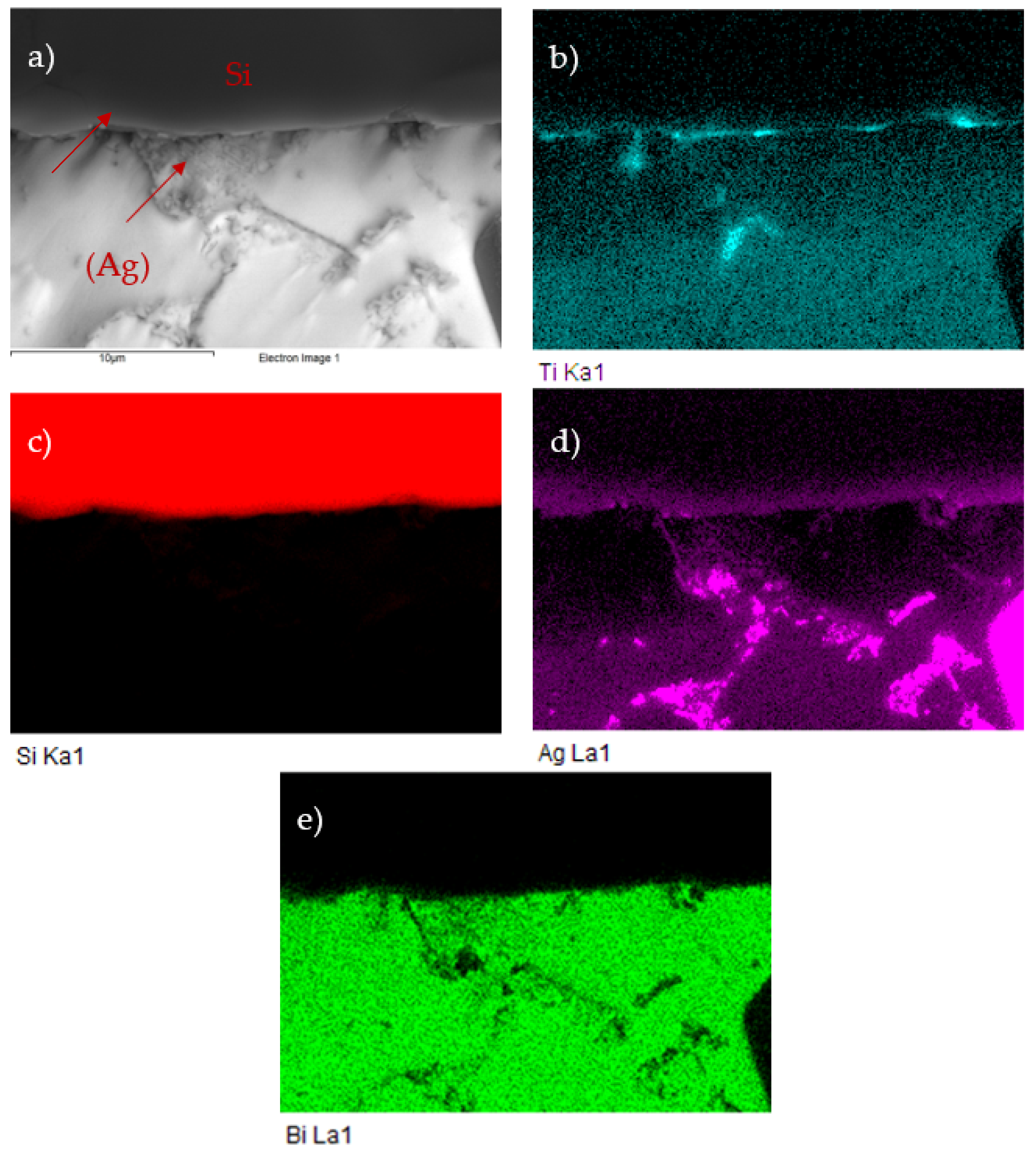
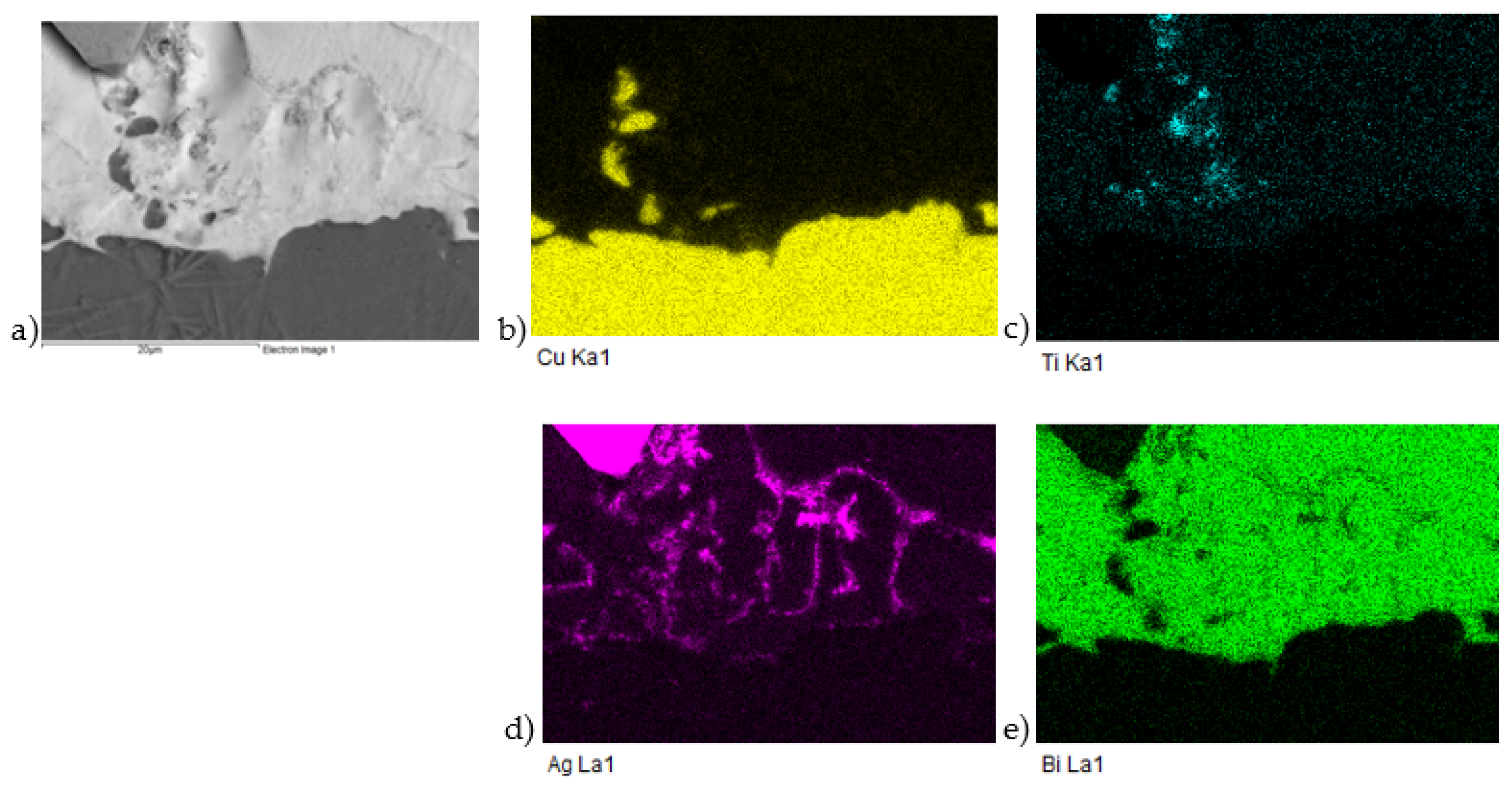
The planar distribution of elements in the boundary is documented in Figure 15. From the planar distribution (Figure 15b) it is obvious that Ti significantly contributes to bond formation, together with silver (Figure 15d).
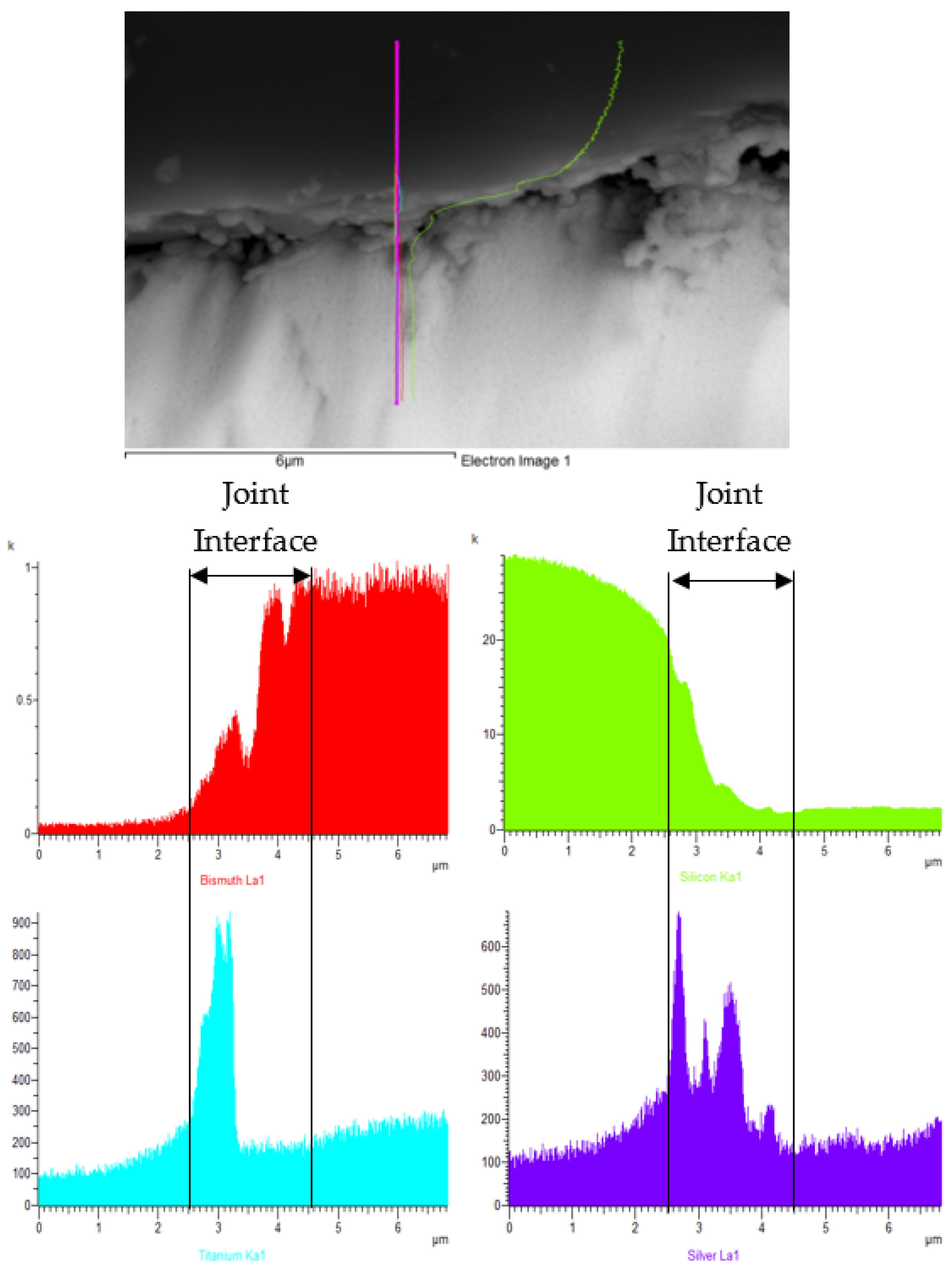
The line analyses (Figure 16) present the concentration profile through the Si/solder boundary in an overall length of 7 μm. The interaction of the solder melt with the Si substrate occurred during soldering only scarcely. Silver in the solder occurred on the grain boundaries of the solidified Bi solder, but also in the boundary of the Si/solder joint. Titanium in the solder is in a minor amount shown in the form of local spots (Figure 15b) on the X-ray maps and was observed also directly in the boundary as a very thin layer, approximately 1 µm thick.
From the mentioned facts, the following mechanism of bond formation may be assumed (Figure 17). In the soldering process, titanium is distributed from the solder to the boundary with silicon, where a reaction layer is formed, ensuring the wetting of silicon. Between the active element and the silicon, a reaction takes place with the formation of reaction products, which allow the wetting of the ceramics with the active solder.
3.6. Analysis of Transition Zone in Cu/Bi11Ag1.5Ti Joint
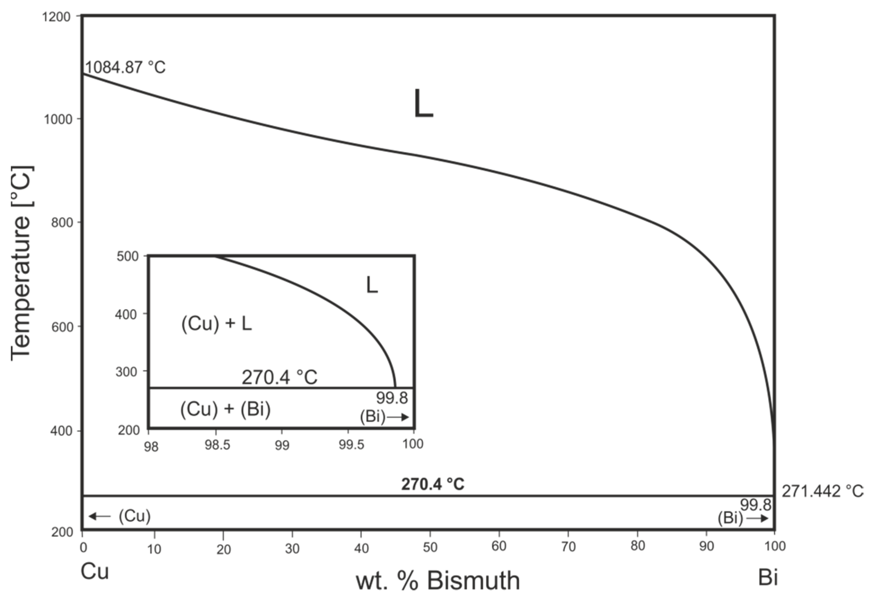
The transition zone of the joint was mainly analysed (Figure 18). The interaction between the molten bismuth solder and copper substrate, supported by a eutectic reaction, occurred in the boundary of the Cu/Bi11Ag1.5Ti joint. According to the Bi-Cu binary diagram, the eutectic reaction takes place at the temperature of 270.6 °C and at a concentration of 99.5 at.% Bi. The mutual solubility is very limited, on both the Bi and also the Cu side (Figure 19). The undulating character of the boundary with copper substrate is the result of the effects of eutectic reaction and the power ultrasound, which emphasizes the reaction. The width of undulation is 4–6 µm.
The spots for measurement location by EDX analysis were selected at four points—Spectrum 1 to Spectrum 4. At the point of measurement for Spectrum 1, the analysis was performed in the Cu/solder boundary. There was no phase, but the mixture of two elements with the proportion of Cu:Bi = 55:45 occurred in the zone with direct contact between both materials.
At the Spectrum 2 point the analysis was performed in the same way as at the Cu/solder boundary zone, but closer to the Cu substrate. The copper content is therefore higher than the bismuth content and, moreover, also silver has diffused there. Analysis was performed also at the measurement point of Spectrum 3 in the solder zone at an approximate depth of 3 μm from the boundary. There, a high Bi content (97.41 wt. %) was identified and the balance consisted of Cu, which diffused from the Cu substrate to the solder melt. The interaction of Cu with Bi was thus proved.
Analysis was also performed at the measurement point of Spectrum 5 from the solder zone at an approximate depth of 7 μm from the boundary. A region where pure silver occurred on the boundary of Bi grains was observed. The presence of Bi (60 wt. %) stems from the surrounding matrix. Titanium was not observed in that area.
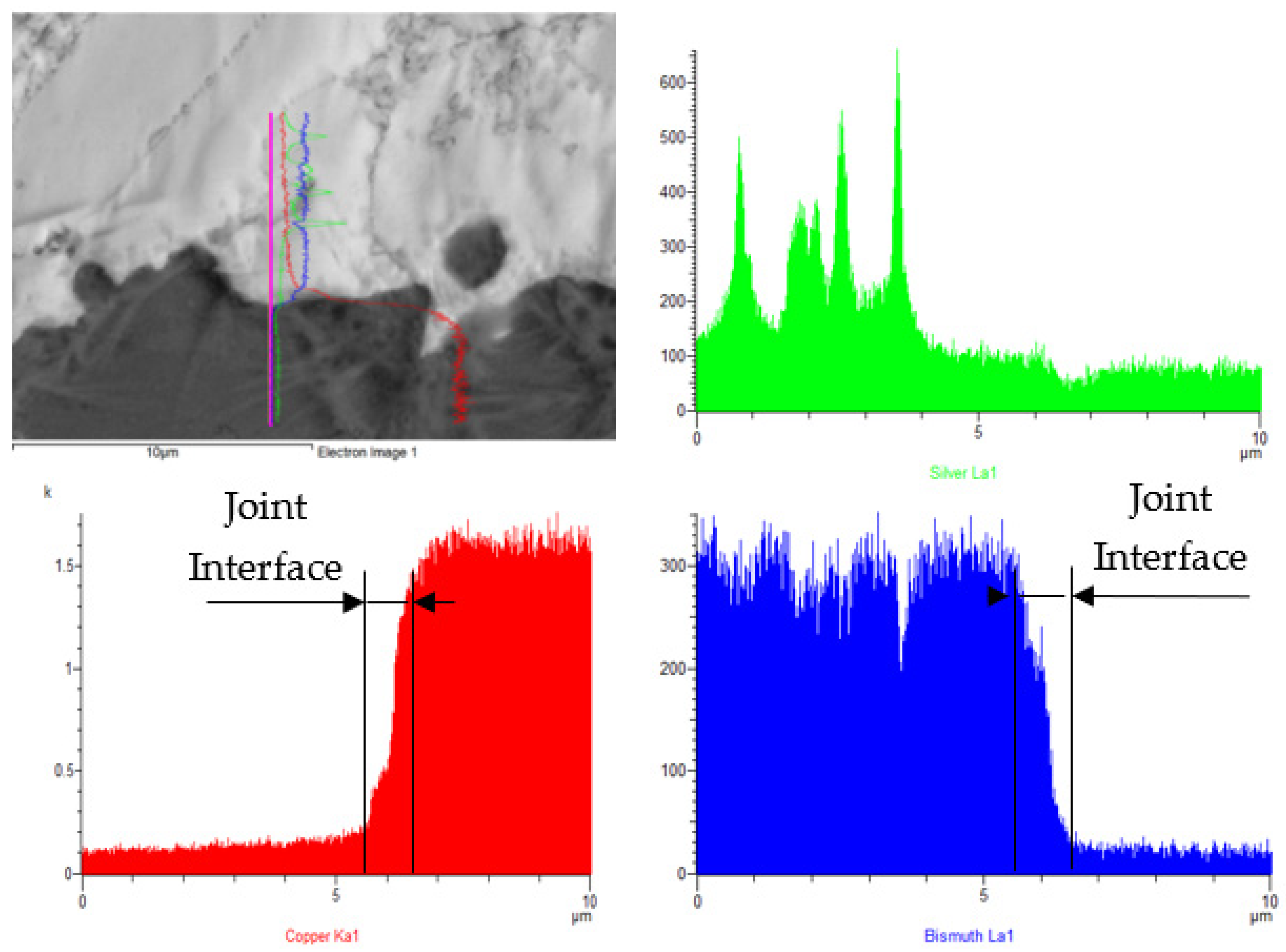
The line analyses (Figure 20) present the concentration profile through the Cu/solder boundary for an overall length of 10 μm. The interaction of the solder melt with the Cu substrate occurred during soldering and the copper was partially dissolved in the solder, owing to diffusion and convection. Silver in the solder occurred on the grain boundaries of the solidified Bi solder in pure elementary form. Titanium (Figure 21c) is contained in the solder as a minor component in the form of local spots revealed by the X-ray map. Bi (Figure 21e) was not observed in the vicinity of the Cu substrate. Silver was partially diffused to the zone of the Cu substrate.
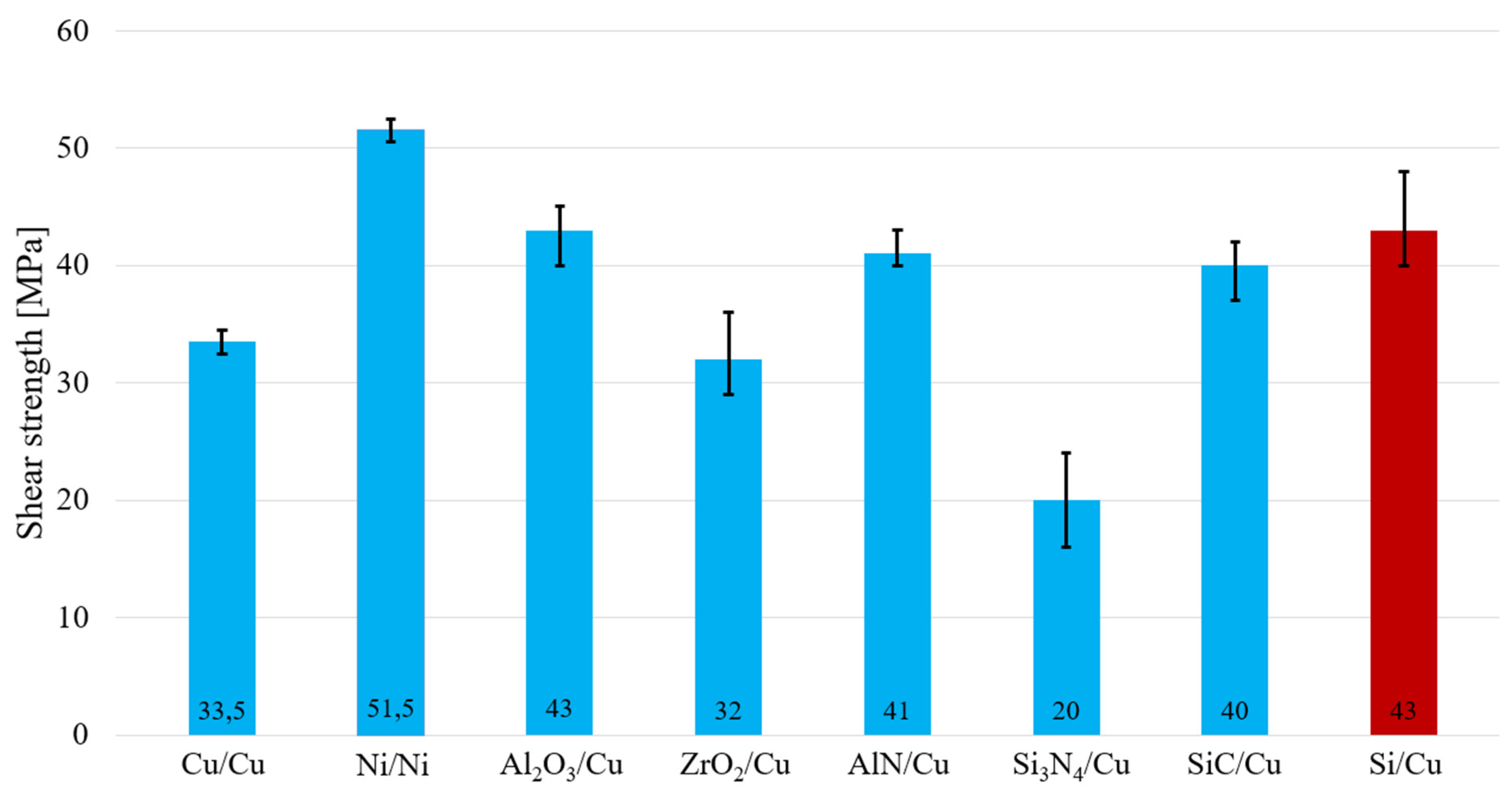
3.7. Shear Strength of Soldered Joints
The research in this work was primarily oriented to the soldering of silicon with copper substrate. Owing to the possibility of application of the active solder type Bi11Ag1.5Ti and its further employment in practice, the testing of the shear strength was extended also to other metallic materials (Cu and Ni), and ceramic materials (Al2O3, ZrO2, AlN, Si3N4, and SiC). The ceramic materials were always tested in combination with copper substrate. The metallic materials were soldered mutually—Cu/Cu and Ni/Ni. Measurement was performed on 6 specimens of each material. The results of the average shear strength are documented in Figure 22. The red colour represents the solder joint examined in this paper. The highest average shear strength in the case of a non-metal/metal combination was obtained with the Si/Cu joint, similarly to the case of the Al2O3/Cu joint combination—43 MPa. In the case of other combinations with ceramic materials, Si3N4/Cu, ZrO2/Cu, SiC/Cu, and AlN/Cu, the average shear strength obtained varied from 20–41 MPa. In the case of metallic materials, the highest average tensile strength was obtained in the joint of two nickel materials, namely 51.5 MPa. In the case of Cu/Cu joints, the average shear strength was 33.5 MPa.
The mentioned results suggest that the strength of silicon/Cu and ceramics/Cu joints fabricated using Bi11Ag1.5Ti solder is comparable with the strength of metal/metal joints. This is caused by the excellent wettability of titanium-containing solder on the ceramic materials with ultrasound activation.
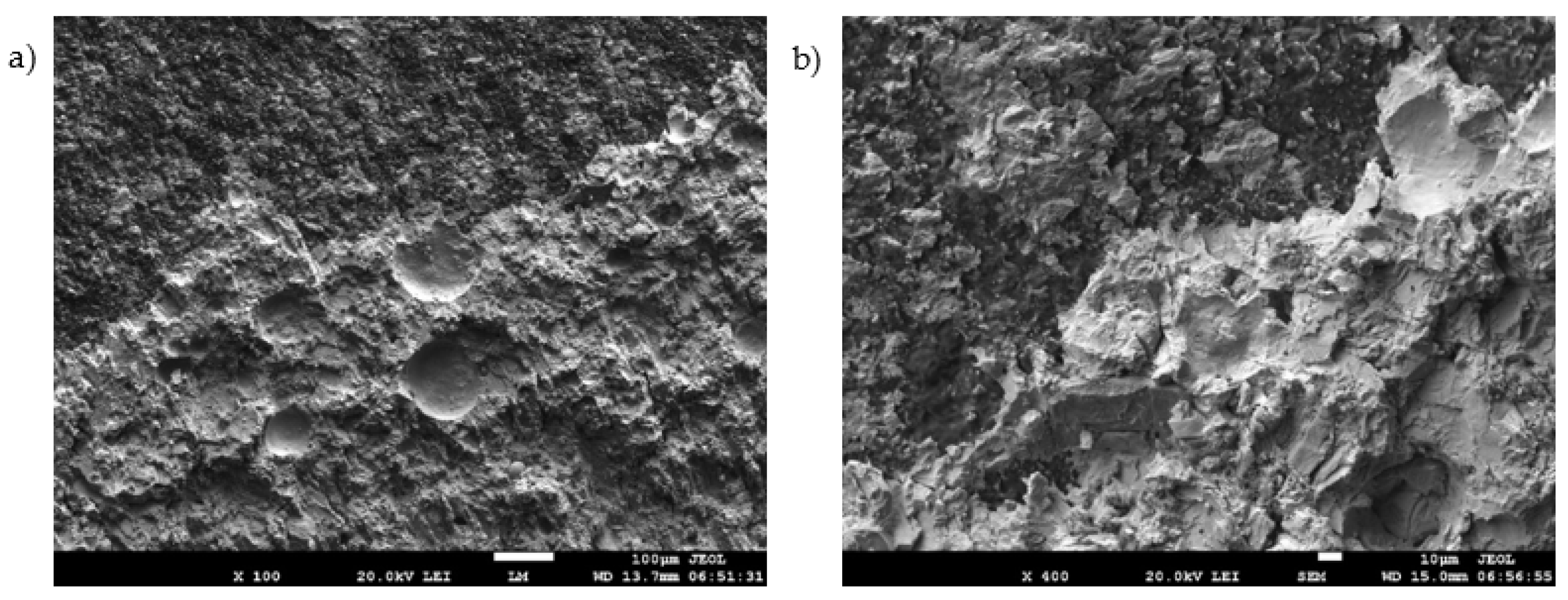
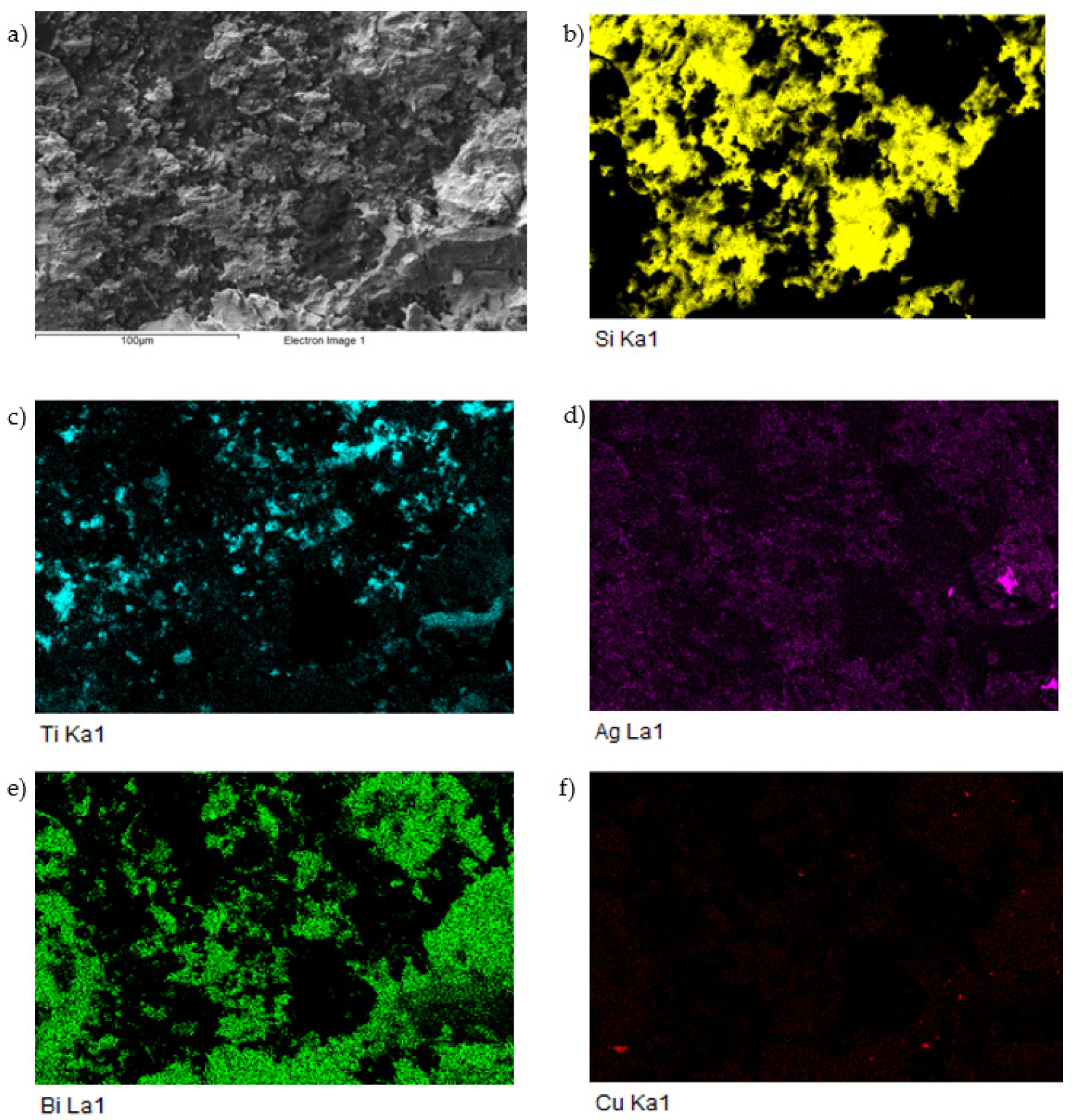
For a more precise identification of bond formation, the fractured surfaces of joints were also analysed. Figure 23a,b shows the fractured surface in the boundary of the Si/Bi11Ag1.5Ti/Cu joint. It can be seen that the fractured surface from the silicon side remained partially covered with solder. Ductile fracture occurred in the solder. The analysis of the planar distribution of the Si, Ti, Ag, Bi, and Cu elements was performed on the fractured surface, as documented in Figure 24b–f. In the case of the planar distribution of Si element, which in Figure 24b represents the parent metal–silicon, local spots can be seen where tearing off of the solder from the substrate has occurred. The planar distribution of Ti on the Si substrate is documented in Figure 24c, where it is obvious that the titanium is segregated on the surface of the Si substrate.
4. Conclusions
The aim of the research was to characterize the soldering alloy type Bi-Ag-Ti. It was studied whether the supposed composition of the soldering alloy is suitable for soldering silicon and copper when applying the soldering process with ultrasound assistance. The following results were achieved:
- For determination of the melting point of the solder, TG/DTA analysis was applied. Three significant temperatures of phase transformation were observed. At the temperature from 401–405 °C, the Bi11Ag1.5Ti alloy precedes the liquidus temperature. At the next stage, at 355 °C, the silver segregation starts with approximately 2 at.%Bi. The last stage comprises the eutectic reaction of the solid solutions (Ag) + (Bi).
- The solder matrix contains bismuth with a local eutectic. The crystals of solid solution of silver (Ag) and intermetallic phases of titanium, BiTi2 and Bi9Ti8, are segregated in the solder matrix.
- The solder type Bi11Ag1.5Ti attains the average tensile strength of 42 MPa. The tensile strength is partially increased by solder alloying with silver and titanium.
- The silicon/solder bond is formed due to titanium interaction with the silicon surface as follows: The titanium, in the soldering process, is distributed to the boundary with silicon due to the effect of ultrasound activity, where a very thin continuous layer roughly 1 µm thick is formed, which ensures the wettability of the silicon. The high titanium and silicon content indicates the interaction with silicon at the formation of probable TiSi2 phase.
- In the boundary of the Cu/solder joint, an interaction between the molten bismuth solder and copper substrate occurs, supported by eutectic reaction. The mutual solubility is very limited, on both the Bi side and the Cu side.
- The measurement of shear strength was performed on a broad range of metallic and ceramic materials. The average shear strength in a combined joint of Si/Cu fabricated with Bi11Ag1.5Ti solder was 43 MPa. The measurement results showed that the strength of non-metal/metal joints is comparable with the strength of metal/metal joints. This is caused by the excellent wettability of solder with active titanium content on the non-metallic and ceramic materials under ultrasound activation.
Author Contributions
Conceptualization, R.K. and I.K.; methodology, R.K.; validation, R.K., I.K. and J.D.; formal analysis, J.D., P.B. and P.G.; investigation, R.K. and I.K.; data curation, I.K.; writing—original draft preparation, R.K.; writing—review and editing, I.K.; visualization, I.K.; supervision, R.K.; project administration, I.K. All authors have read and agreed to the published version of the manuscript.
Funding
This work was supported by the Slovak Research and Development Agency under the contract no. APVV-17-0025. The paper was also prepared with the support of the VEGA 1/0303/20: Research of joining metallic and ceramic materials in production of power semiconductor; Project 1393–Soldering–Excellent teams and project Young Researcher excellent teams no. 1392.
Informed Consent Statement
Informed consent was obtained from all subjects involved in the study.
Data Availability Statement
The data presented in this study are available on request from the corresponding author.
Acknowledgments
The paper was also prepared in cooperation with the VSB-Technical University of Ostrava, FMT-Faculty of Materials Science and Technology, Department of Non-ferrous Metals, Refining and Recycling.
Conflicts of Interest
The authors declare no conflict of interest.
References
- Vianco, P.T. Solder technology for ultrahigh temperatures. Weld. J. 2002, 81, 51–54. [Google Scholar]
- Urbikain, G.; Perez, J.M.; López de Lacalle, L.N.; Andueza, A. Combination of friction drilling and form tapping processes on dissimilar materials for making nutless joints. Proc. Inst. Mech. Eng. Part B J. Eng. Manuf. 2018, 232, 1007–1020. [Google Scholar] [CrossRef]
- Kang, U.-B.; Kim, Y.-H. A new COG technique using low temperature solder bumps for LCD driver IC packaging applications. IEEE Trans. Compon. Packag. Technol. 2004, 27, 253–258. [Google Scholar] [CrossRef]
- Mei, Z.; Holder, H.; Plas, H.V. Hewlett-Packard. HP J. 1996, 48, 91. [Google Scholar]
- Suh, M.-S.; Park, C.-J.; Kwon, H.-S. Effects of plating parameters on alloy composition and microstructure of Sn–Bi electrodeposits from methane sulphonate bath. Surf. Coat. Technol. 2006, 200, 3527–3532. [Google Scholar] [CrossRef]
- Ren, G.; Wilding, I.J.; Collins, M.N. Alloying influences on low melt temperature SnZn and SnBi solder alloys for electronic interconnections. J. Alloy Compd. 2016, 665, 251–260. [Google Scholar] [CrossRef]
- Kang, N.; Na, H.S.; Kim, S.J.; Kang, C.Y. Alloy design of Zn–Al–Cu solder for ultra high temperatures. J. Alloy Compd. 2009, 467, 246–250. [Google Scholar] [CrossRef]
- Mahmudi, R.; Alibabaie, S. Elevated-temperature shear strength and hardness of Zn–3Cu–xAl ultra-high-temperature lead-free solders. Mater. Sci. Eng. A 2013, 559, 421–426. [Google Scholar] [CrossRef]
- Alibabaie, S.; Mahmudi, R. Microstructure and creep characteristics of Zn–3Cu–xAl ultra high-temperature lead-free solders. Mater. Des. 2012, 39, 397–403. [Google Scholar] [CrossRef]
- Gancarz, T.; Pstruś, J.; Fima, P.; Mosińska, S. Thermal properties and wetting behavior of high temperature Zn-Al-In solders. J. Mater. Eng. Perform. 2012, 21, 599–605. [Google Scholar] [CrossRef] [Green Version]
- Mallick, S.; Kabir, M.S.; Sharif, A. Study on the properties of Zn–xNi high temperature solder alloys. J. Mater. Sci. Mater. Electron. 2016, 27, 3608–3618. [Google Scholar] [CrossRef]
- Xian, A.P. Wetting of Si-Al-O-N ceramic by Sn-5at.%Ti-X ternary active solder. Mater. Sci. Eng. B 1994, 25, 39–46. [Google Scholar] [CrossRef]
- Wei, P.; Li, J.; Chen, J. Titanium metallization of Si3N4 ceramics by molten salt reaction: Coating microstructure and brazing property. Thin Solid Film. 2002, 422, 126–129. [Google Scholar] [CrossRef]
- Walker, C.A.; Hodges, V.C. Comparing metal-ceramic brazing methods. Weld. J. 2008, 87, 43–50. [Google Scholar]
- Yu, W.-Y.; Liu, S.-H.; Liu, X.-Y.; Liu, M.-P.; Shi, W.-G. Interface reaction in ultrasonic vibration-assisted brazing of aluminum to graphite using Sn–Ag–Ti solder foil. J. Mater. Process. Technol. 2015, 221, 285–290. [Google Scholar] [CrossRef]
- Kui, Y.F.; Kui, M.D.; Xin, J.L.; Hui, X.H.; Xu, H.P. Brazing sapphire/sapphire and sapphire/copper sandwich joints using Sn-Ag-Ti active solder alloy. Solid State Phenom. 2018, 273, 187–193. [Google Scholar] [CrossRef]
- Yu, W.-Y.; Liu, Y.; Liu, X.-Y. Spreading of Sn-Ag-Ti and Sn-Ag-Ti(-Al) solder droplets on the surface of porous graphite through ultrasonic vibration. Mater. Des. 2018, 150, 9–16. [Google Scholar] [CrossRef]
- Chang, S.Y.; Chuang, T.H.; Tsao, L.C.; Yang, C.L.; Yang, Z.S. Active soldering of ZnS–SiO2 sputtering targets to copper backing plates using an Sn3.5Ag4Ti(Ce, Ga) filler metal. J. Mater. Process. Technol. 2008, 202, 22–26. [Google Scholar] [CrossRef]
- Chang, S.Y.; Tsao, L.C.; Chiang, M.J.; Chuang, T.H.; Tung, C.N.; Pan, G.H. Active soldering of indium tin oxide (ITO) with Cu in air using an Sn3.5Ag4Ti(Ce, Ga) filler. J. Mater. Eng. Perform. 2003, 12, 383–389. [Google Scholar] [CrossRef]
- Qu, W.; Zhou, S.-S.; Zhuang, H.-S. Effect of Ti content and Y additions on oxidation behavior of SnAgTi solder and its application on dissimilar metals soldering. Mater. Des. 2015, 88, 737–742. [Google Scholar] [CrossRef]
- Koleňák, R.; Kostolný, I.; Drápala, J.; Kusý, M.; Pašák, M. Research on soldering AlN ceramics with Cu substrate using Sn-Ag-Ti solder. Solder Surf. Mount Technol. 2019, 31, 93–101. [Google Scholar] [CrossRef]
- Weber, F.; Rettenmayr, M. Joining of SiO2 glass and 316L stainless steel using Bi–Ag-based active solders. J. Mater. Sci. 2021, 56, 3444–3454. [Google Scholar] [CrossRef]
- Kolenak, R.; Kostolny, I. Study of direct bonding ceramics with metal using Sn2La solder. Adv. Mater. Sci. Eng. 2015, 2015, 1–13, ISSN 1687-8434. [Google Scholar] [CrossRef] [Green Version]
- Kolenak, R.; Kostolny, I.; Drápala, J.; Sahul, M.; Urminský, J. Characterizing the soldering alloy type In–Ag–Ti and the study of direct soldering of SiC ceramics and copper. Metals 2018, 8, 274. [Google Scholar] [CrossRef] [Green Version]
- Koleňák, R.; Šebo, P.; Provazník, M.; Koleňáková, M.; Ulrich, K. Shear strength and wettability of active Sn3.5Ag4Ti (Ce,Ga) solder on Al2O3 ceramics. Mater. Des. 2011, 32, 3997–4003. [Google Scholar] [CrossRef]
- Cheng, L.X.; Li, G.Y.; Li, Z.L.; Wu, Z.Z.; Zhou, B. Effects of titanium on active bonding between Sn3. 5Ag4Ti (Ce, Ga) alloy filler and alumina. J. Mater. Sci. Mater. Electron. 2015, 26, 6004–6012. [Google Scholar] [CrossRef]
- Tsao, L.C. Interfacial structure and fracture behavior of 6061 Al and MAO-6061 Al direct active soldered with Sn–Ag–Ti active solder. Mater. Des. 2014, 56, 318–324. [Google Scholar] [CrossRef]
- Tsao, L.C. Microstructural characterization and mechanical properties of microplasma oxidized TiO2/Ti joints soldered using Sn3.5Ag4Ti (Ce) active filler. J. Mater. Sci. Mater. Electron. 2014, 25, 233–243. [Google Scholar] [CrossRef]
- Yu, W.-Y.; Liu, S.H.; Liu, X.Y.; Shao, J.L.; Liu, M.P. Wetting behavior in ultrasonic vibration-assisted brazing of aluminum to graphite using Sn-Ag-Ti active solder. Surf. Rev. Lett. 2015, 22, 1550035. [Google Scholar] [CrossRef]
- Massalski, T.B. Binary Alloy Phase Diagrams; ASM, Metals Park: Cleveland, OH, USA, 1996. [Google Scholar]
- Okamoto, H. Bi–Ti (Bismuth–Titanium). J. Phase Equilibria Diffus. 2010, 31, 314–315. [Google Scholar] [CrossRef]
Figure 1.
Test piece of solder for the static tensile test (unit: mm).

Figure 2.
Assembly of soldered joint: (a) for analysis of solder/substrate joint; (b) for shear strength measurement.
Figure 2.
Assembly of soldered joint: (a) for analysis of solder/substrate joint; (b) for shear strength measurement.

Figure 3.
Schematic representation of ultrasonic activation on the substrate surface.

Figure 4.
Schematic representation of shear strength measurement with a special jig.

Figure 5.
TG/DTA analysis of Bi11Ag1.5Ti solder, heating rate of 5 °C/min, second heating.

Figure 6.
Equilibrium binary diagram of silver–bismuth system [30] with marked transformation of T1.
Figure 6.
Equilibrium binary diagram of silver–bismuth system [30] with marked transformation of T1.

Figure 7.
Microstructure of Bi11Ag1.5Ti solder after etching viewed by the optical microscope.

Figure 8.
Point EDX analysis of Bi11Ag1.5Ti solder.

Figure 9.
XRD analysis of Bi11Ag1.5Ti solder.

Figure 10.
Map of Ag, Ti, and Bi elements in microstructure of Bi11Ag1.5Ti solder.

Figure 11.
Microstructure of boundary in Si/Bi11Ag1.5Ti/Cu joint from SEM in BSE (backscattered electron) mode.
Figure 11.
Microstructure of boundary in Si/Bi11Ag1.5Ti/Cu joint from SEM in BSE (backscattered electron) mode.

Figure 12.
Point EDX analysis of Si/Bi11Ag1.5Ti joint.

Figure 13.
Equilibrium binary diagram of Ti-Si [30].
Figure 13.
Equilibrium binary diagram of Ti-Si [30].

Figure 14.
Equilibrium binary diagram of Ti-Ag [30].
Figure 14.
Equilibrium binary diagram of Ti-Ag [30].

Figure 15.
Planar distribution of Ti, Si, Ag, and Bi elements in the boundary of Si/Bi11Ag1.5Ti joint. (a) joint microstructure (b) Ti (c) Si (d) Ag (e) Bi.
Figure 15.
Planar distribution of Ti, Si, Ag, and Bi elements in the boundary of Si/Bi11Ag1.5Ti joint. (a) joint microstructure (b) Ti (c) Si (d) Ag (e) Bi.

Figure 16.
Line EDX analysis of Si/Bi11Ag1.5Ti joint and the concentration profiles of Bi, Si, Ti, and Ag elements.
Figure 16.
Line EDX analysis of Si/Bi11Ag1.5Ti joint and the concentration profiles of Bi, Si, Ti, and Ag elements.

Figure 17.
Mechanism of bond formation.

Figure 18.
Point EDX analysis of boundary in Cu/Bi11Ag1.5Ti joint.

Figure 19.
Equilibrium binary diagram of Cu-Bi [30].
Figure 19.
Equilibrium binary diagram of Cu-Bi [30].

Figure 20.
Line EDX analysis of Cu/Bi11Ag1.5Ti joint and the concentration profiles of Cu, Ag, and Bi elements.
Figure 20.
Line EDX analysis of Cu/Bi11Ag1.5Ti joint and the concentration profiles of Cu, Ag, and Bi elements.

Figure 21.
Map of Cu, Ti, Ag, and Bi elements in the boundary of Cu/Bi11Ag1.5Ti. (a) joint microstructure (b) Cu (c) Ti (d) Ag (e) Bi.
Figure 21.
Map of Cu, Ti, Ag, and Bi elements in the boundary of Cu/Bi11Ag1.5Ti. (a) joint microstructure (b) Cu (c) Ti (d) Ag (e) Bi.

Figure 22.
Shear strength of soldered joints fabricated with Bi11Ag1.5Ti solder.

Figure 23.
Fractured surface of soldered joint of Si/BiAg11Ti1,5/Cu (a) magnification 100×; (b) magnification 400×.
Figure 23.
Fractured surface of soldered joint of Si/BiAg11Ti1,5/Cu (a) magnification 100×; (b) magnification 400×.

Figure 24.
Fractured surface of soldered joint of Si/BiAg11Ti1,5/Cu and the planar distribution of elements (a) fracture structure; (b) Si; (c) Ti; (d) Ag; (e) Bi; (f) Cu.
Figure 24.
Fractured surface of soldered joint of Si/BiAg11Ti1,5/Cu and the planar distribution of elements (a) fracture structure; (b) Si; (c) Ti; (d) Ag; (e) Bi; (f) Cu.


Table 1.
Composition of Bi-Ag-Ti alloy and the results of chemical analysis by ICP-AES method [wt. %].
Table 1.
Composition of Bi-Ag-Ti alloy and the results of chemical analysis by ICP-AES method [wt. %].
| Sample | Charge [wt. %] | ICP-AES [wt. %] | ||||
|---|---|---|---|---|---|---|
| Bi | Ag | Ti | Bi | Ag | Ti | |
| Bi11Ag1.5Ti | 87.5 | 11.0 | 1.5 | balance | 10.5 ± 0.2 | 1.24 ± 0.17 |
Table 2.
Soldering parameters.
| Ultrasound power | 400 | [W] |
| Working frequency | 40 | [kHz] |
| Amplitude | 2 | [μm] |
| Soldering temperature | 380 | [°C] |
| Time of ultrasound activation | 5 | [s] |
Table 3.
Significant temperatures of phase transformations determined by TG/DTA analysis.
| DTA Analysis | TL (°C) | T1 (°C) | TE (°C) | |
|---|---|---|---|---|
| Heating | 1st | 405 | 351 | 264 |
| 2nd | 401 | 355 | 262 | |
TL–liquidus temperature; T1–temperature of transformation shown in Figure 6; TE–temperature of eutectic transformation.
Publisher’s Note: MDPI stays neutral with regard to jurisdictional claims in published maps and institutional affiliations. |
© 2021 by the authors. Licensee MDPI, Basel, Switzerland. This article is an open access article distributed under the terms and conditions of the Creative Commons Attribution (CC BY) license (https://creativecommons.org/licenses/by/4.0/).
Share and Cite
MDPI and ACS Style
Kolenak, R.; Kostolny, I.; Drapala, J.; Babincova, P.; Gogola, P. Characterization of Soldering Alloy Type Bi-Ag-Ti and the Study of Ultrasonic Soldering of Silicon and Copper. Metals 2021, 11, 624. https://doi.org/10.3390/met11040624
AMA Style
Kolenak R, Kostolny I, Drapala J, Babincova P, Gogola P. Characterization of Soldering Alloy Type Bi-Ag-Ti and the Study of Ultrasonic Soldering of Silicon and Copper. Metals. 2021; 11(4):624. https://doi.org/10.3390/met11040624
Chicago/Turabian StyleKolenak, Roman, Igor Kostolny, Jaromir Drapala, Paulina Babincova, and Peter Gogola. 2021. "Characterization of Soldering Alloy Type Bi-Ag-Ti and the Study of Ultrasonic Soldering of Silicon and Copper" Metals 11, no. 4: 624. https://doi.org/10.3390/met11040624
Note that from the first issue of 2016, this journal uses article numbers instead of page numbers. See further details here.