
Abstract
Carrier mobility is one of the most fundamental material parameters of semiconductors and requisite for device applications and interpretation of physical phenomena. We determined the electron and hole mobilities of a CH3NH3PbBr3 single crystal in the high-carrier density regime by combining AC Hall measurements under photoexcitation and two-carrier analysis. Both electron and hole mobilities were significantly enhanced by photo-doping and exceeded 300 cm2 V−1 s−1, which are comparable to the electron Hall mobilities of conventional inorganic semiconductors. Our experimental results indicate that charged dislocation scattering dominates the carrier transport at room temperature in the low-carrier density regime.
Export citation and abstract BibTeX RIS

Content from this work may be used under the terms of the Creative Commons Attribution 4.0 license. Any further distribution of this work must maintain attribution to the author(s) and the title of the work, journal citation and DOI.
The excellent material properties of halide perovskite semiconductors have been long exploited for various optoelectronic devices, including solar cells, LEDs, photodetectors, light modulators, nonlinear devices, and quantum emitters. 1–7) The considerably long carrier lifetimes and high luminescence efficiencies of halide perovskite semiconductors due to the low nonradiative recombination rate is a remarkable feature, which gives rise to unique phenomena such as photon recycling. 8) Numerous studies have demonstrated that halide perovskites are one of the best quality semiconductors, even when compared with conventional inorganic semiconductors.
Despite their excellent optical properties, the carrier transport of halide perovskites is considered to be relatively poor; the reported Hall mobility is typically in the order of several tens of cm2 V−1 s−1,
9–14) which is much lower than that of conventional inorganic semiconductors (e.g. 9400 cm2 V−1 s−1 for electrons in GaAs).
15) Such moderate carrier mobilities have been discussed in terms of polarons, which are self-localized carriers formed through electron–phonon coupling.
16–18) Polaron formation enhances the carrier mass, resulting in reduced carrier mobility. Halide perovskites exhibit strong electron–phonon coupling considering the higher Fröhlich coupling constant (α  1.8 for CH3NH3PbBr3),
16) compared with that of conventional semiconductors (e.g. α = 0.06 for GaAs and α = 0.40 for ZnSe).
19) In addition, its soft lattice nature might further enhance the polaron effect.
17,20) Detailed polaron formation mechanisms, such as conventional Fröhlich large polarons, small polarons, and ferroelectric-like polarons, have been discussed to evaluate the impact of polarons on the carrier transport properties of semiconductors.
16–18,20) However, this issue remains under active debate.
1.8 for CH3NH3PbBr3),
16) compared with that of conventional semiconductors (e.g. α = 0.06 for GaAs and α = 0.40 for ZnSe).
19) In addition, its soft lattice nature might further enhance the polaron effect.
17,20) Detailed polaron formation mechanisms, such as conventional Fröhlich large polarons, small polarons, and ferroelectric-like polarons, have been discussed to evaluate the impact of polarons on the carrier transport properties of semiconductors.
16–18,20) However, this issue remains under active debate.
To address this issue, the intrinsic carrier mobility must be evaluated. Although numerous studies have focused on the carrier mobility of halide perovskites using various measurement techniques, the reported mobility is spread over a wide range (for instance, from 8 to 220 cm2 V−1 s−1 for CH3NH3PbBr3). 10,11,14,21) Theoretical calculations have also reported various values. 17,22–28) Some possible mechanisms that hinder the evaluation of intrinsic carrier mobility can be suggested. One such mechanism is the highly insulating nature of halide perovskites. Sufficient carrier doping by ion substitution has not been successful in this class of materials. 12) Therefore, previous Hall measurements reported a very small carrier density (109–1011 cm−3) due to unintentional doping. 9–11,13) In the case of such a small carrier density and the resulting low electronic conductivity, accurately estimating the carrier mobility becomes challenging. More intriguingly, very high electron Hall mobility exceeding 2000 cm2 V−1 s−1 has been reported for a heavily doped CH3NH3SnI3 crystal (carrier density ∼1014 cm−3), 29) which implies that the carrier mobility depends on the carrier density. In this case, high-density carriers are essential for obtaining an intrinsic carrier mobility. Another factor is the extrinsic carrier scattering by impurities or at the grain boundary, 30) which should be more prominent for solution-processed thin films. Ferroelastic twin boundaries might also disturb carrier transport. 31) These issues can be overcome using high-quality single crystals in the cubic phase.
In this study, we aimed to evaluate the intrinsic carrier mobility of a cubic-phase CH3NH3PbBr3 single crystal at room temperature. We performed an AC Hall measurement on a high-quality single crystal under light illumination and the data were analyzed by two carrier model. These enabled us to evaluate the intrinsic carrier mobilities of electrons and holes independently. Our results highlight the excellent carrier transport properties of halide perovskites, which are crucial for perovskite-based device applications, and provide essential insights for fundamental semiconductor physics.
CH3NH3PbBr3 single crystals were grown by a modified anti-solvent vapor-assisted crystallization technique. We thinned the crystal up to 50 μm and polished the surface (see supplementary data available online at stacks.iop.org/APEX/14/041009/mmedia). To perform reliable conductivity measurements, the contact resistance between semiconductors and electrodes must be reduced. For this purpose, we utilized rubrene as an intermediate layer material. As shown in the inset of Fig. 1(a), we evaporated rubrene (328 nm) and Au (40 nm) at the four corners of the sample. Figure 1 shows the two-terminal current–voltage curves measured in the CH3NH3PbBr3 single crystals under room light irradiation using contacts with a rubrene intermediate layer (red curve) and only Au metal (black curve). The contact resistance between the sample surface and the Au electrode was significantly reduced by the rubrene layer.
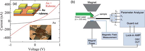
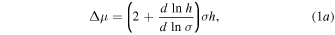
Fig. 1. (Color online) (a) Two-terminal current–voltage curves for the CH3NH3PbBr3 single crystals measured using Au electrodes and Au/Rubrene electrodes. The inset shows a schematic illustration of the four-contact probe experiment (upper) and a photograph of the sample and electrodes (lower). (b) Schematic diagram of the experimental setup.
Download figure:
Standard image High-resolution imageConductivity measurements were performed by the four-probe method in the van der Pauw configuration. We adopted the AC-Hall technique that allows low-noise measurement by an AC magnetic field and lock-in detection system. 32) The frequency of the alternating magnetic field was 0.1 Hz, which was generated by applying sine-wave AC current to reduce the harmonic components. The experimental configuration is schematically shown in Fig. 1(b) (see supplementary data). Because our sample is almost insulated under dark conditions, we illuminated the sample from the electrode side by a green laser (center wavelength = 555 nm) to enhance the carrier density. The penetration depth at 555 nm was approximately 100 μm. 33) It is advantageous to use photoexcitation for easily controlling the carrier density. However, the analysis to estimate the carrier mobility in the case of photo-doping is more complicated than standard single-carrier analysis. The detailed analysis method is described below.
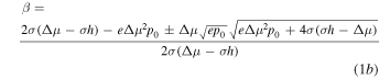
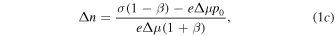
We analyzed the data obtained by the AC Hall measurement under photoexcitation using a two-carrier model, which was recently proposed by Gunawan et al.
32) In the presence of both electrons and holes in semiconductors, the conductivity (σ) and Hall coefficient (h) can be given as  and
and  where n (p) and
 are the electron (hole) density and mobility, respectively. Here, we define
  Assuming that the sample is a p-type semiconductor under dark conditions, the carrier density should be
  where
where  is the hole density in the dark and
  represents the electron (hole) density generated by photoexcitation. If we can assume
  the following three equations are obtained:
where  From the experimentally obtained h,
  and
and  we can determine the electron and hole mobilities independently. The above procedure was formulated under the assumption of a constant
  Therefore, we further made a correction to obtain correct carrier mobilities according to the procedure proposed by Gunawan et al.
32) Note that the mobility values were not significantly modified by this correction.
Therefore, we further made a correction to obtain correct carrier mobilities according to the procedure proposed by Gunawan et al.
32) Note that the mobility values were not significantly modified by this correction.
First, we conducted Hall measurements in the dark. We confirmed that the sample was a p-type semiconductor and determined  =
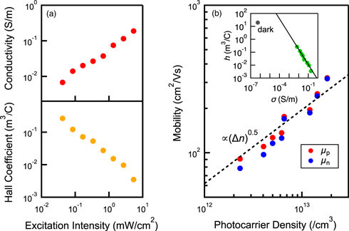
=  cm−3 based on an analysis by a standard single-carrier model. Here, the hole mobility was estimated to be 0.11 cm2 V−1 s−1. Note that the carrier density and the mobility in the dark show a large sample-to-sample dependence (see supplementary data), while we confirmed the negligibly small measurement-to-measurement difference. Figure 2(a) displays the Hall coefficient and conductivity as a function of the excitation light intensity. As the excitation intensity increased, the electronic conductivity was sublinearly enhanced, whereas the Hall coefficient was reduced.
Fig. 2. (Color online) (a) Electronic conductivity and Hall coefficient as a function of the excitation light intensity. (b) Electron and hole mobilities as a function of the photocarrier density. The dotted line corresponds to the square root of the photocarrier density. The inset shows a plot of ln h versus ln σ. Hole mobility measured in dark is also plotted for reference. The solid line corresponds to the fitting result by power law.
Download figure:
Standard image High-resolution image
We analyzed the data based on the two-carrier model. A plot of ln h versus ln σ is shown in the inset of Fig. 2(b). Note that the conductivity and Hall mobility measured under dark conditions are also plotted in the same figure for reference purposes. The ln h versus ln σ curve shows almost linear dependence, as indicated by the solid line. We estimated  from the slope of this line, which enables us to determine μn and μp from Eqs. (1a
)–(1c
).
from the slope of this line, which enables us to determine μn and μp from Eqs. (1a
)–(1c
).
Figure 2(b) shows the electron and hole mobilities as a function of the photocarrier density. With an increase in the photocarrier density, the mobilities were significantly enhanced. Note that when in a previous study, AC Hall measurement was performed in a solution-processed mixed perovskite thin film, a similar increasing trend was reported, 32) whereas the mobility value was two orders of magnitude lower than our reported result. We consider that the discrepancy is due to the high-concentration grain boundaries in solution-processed thin films.
Under intense photoexcitation, β approaches almost unity, indicating similar effective masses for electrons and holes. The electron and hole mobilities reached μn = 318 cm2 V−1 s−1 and μp = 322 cm2 V−1 s−1 at the maximum. According to the increasing trend shown in Fig. 2(b), the carrier mobility is most likely to increase further with carrier density. Notably, the injection of high-density photocarriers becomes more difficult because of photodegradation under intense light irradiation. Interestingly, while the carrier density under a fixed excitation light intensity is reduced after strong light irradiation, we confirmed that the carrier mobility measured at a fixed carrier density was unchanged by photodegradation (see supplementary data). This result indicates that the defects that promote nonradiative recombination are formed by light irradiation, but are irrelevant to the transport properties of photocarriers.
It is meaningful to compare our results with those reported previously. Table I summarizes the reported carrier mobilities of CH3NH3PbBr3 single crystals by various experimental techniques. The carrier densities of halide perovskites in previous reports were typically in the order of 109–1011 cm−3, which are much smaller than the maximum photocarrier density observed here (∼1013 cm−3). In such a low-density regime, it is difficult to evaluate the carrier mobility accurately by conventional Hall measurements. Besides, we demonstrate that the carrier mobility is dependent on carrier density. We consider that the above two factors give rise to the large discrepancy between our results and previous reports of Hall motilities. It is also significant to point out that the photocarrier density in perovskite solar cells and LEDs under working conditions is in the order of 1011–1013 cm−3. 34,35) Therefore, our results are more relevant to actual device operation and highlight the potential of this material in device applications.
Table I. Comparison of previously reported Hall mobilities of CH3NH3PbBr3 single crystals. (TOF: time-of-flight measurements; SCLC: space-charge-limited current measurements.)
| Method | Charge type | Mobility (cm2 V−1 s−1) | Carrier density (cm−3) | References |
|---|---|---|---|---|
| Hall | Electron | 48 | 2.3 × 10¹² | 12 |
| Hole | 20–60 | 5 × 10⁹ –3 × 10¹¹ | 9,11, 13 | |
| SCLC | Electron | 41 | 8.8 × 10¹⁰ | 13 |
| Hole | 24–38 | 5.8 × 10⁹ –1.5 × 10¹¹ | 9,11, 37 | |
| TOF | Electron | 190 | — | 21 |
| Hole | 115–217 | — | 9, 21 | |
| This work | Electron | 318 | 1.8 × 10¹³ | |
| (Photo-Hall) | Hole | 322 | 1.8 × 10¹³ |
Here, we discuss the physical origin of the monotonic increase in mobility with photocarrier density. One possible mechanism is the carrier trapping by impurity states. Under weak excitation, carrier transport might be dominated by the trap-detrap process, where the effective carrier mobility,  can be expressed by
  where τtrap and τfree are the average time spent by carriers in traps and free transport states, respectively.
36) Under high-density photoexcitation, the trap states are almost completely occupied and intrinsic carrier transport can be observed. However, we consider this scenario to be less plausible. As shown in Table I, the reported Hall mobility is significantly lower than the drift mobility by time-of-flight measurements. Because the drift mobility is inherently more sensitive to the carrier trapping process than the Hall mobility, we did not consider that the trap-detrap process determines the carrier transport of halide perovskites.
where τtrap and τfree are the average time spent by carriers in traps and free transport states, respectively.
36) Under high-density photoexcitation, the trap states are almost completely occupied and intrinsic carrier transport can be observed. However, we consider this scenario to be less plausible. As shown in Table I, the reported Hall mobility is significantly lower than the drift mobility by time-of-flight measurements. Because the drift mobility is inherently more sensitive to the carrier trapping process than the Hall mobility, we did not consider that the trap-detrap process determines the carrier transport of halide perovskites.
Rather, we propose carrier scattering by charged dislocations because a similar dependence of mobility on carrier density due to dislocation scattering has been reported in some inorganic semiconductors such as Ge and GaN. 38,39) For n-type GaN, the carrier-density dependent mobility has been explained by a space charge produced by negatively charged dislocations that scatter electrons traveling across dislocations. 39) In this case, the carrier mobility is inversely proportional to the Debye screening length, and thus shows square-root dependence on carrier density. Recently, the role of dislocations in halide perovskites has been underlined in some reports. 40) In addition, the carrier mobility shows square-root dependence, as shown by the dotted line in Fig. 2(b). This result supports the above-mentioned scenario. In this context, it is expected that the carrier mobility is further enhanced by reducing the dislocation density and approaches the intrinsic value dominated purely by phonon scattering. However, it should be pointed out that the small hole mobility in the dark and its rapid increase by light illumination suggest that the other scattering mechanism is dominant in the low-density regime.
Finally, we compared the estimated carrier mobility with those of other inorganic semiconductors. The carrier mobility of ≥300 cm2 V−1 s−1 in CH3NH3PbBr3 estimated here is comparable to the electron Hall mobility of conventional II–VI inorganic semiconductors such as CdS (385 cm2 V−1 s−1), CdSe (605 cm2 V−1 s−1), and ZnSe (530 cm2 V−1 s−1), 41,42) which have bandgap energies similar to those of CH3NH3PbBr3. This result may lead to the conclusion that the polaron effect in halide perovskite is not very strong; at least photocarriers are not affected by the strong carrier localization due to small polaron formation. Moreover, this finding is significant for electronic device applications of this material. Considering that the carrier mobility is enhanced in the high carrier density region, the development of a carrier doping technique is essential to maximizing the potential of this material.
In summary, we report the Hall mobility of CH3NH3PbBr3 single crystals by means of AC Hall measurement and two-carrier analysis, which enabled us to accurately determine the electron and hole mobilities in the high carrier density regime. We evaluated the intrinsic carrier mobility under high-density excitation. We reveal that the electron and hole mobilities monotonically increase with carrier density and exceed 300 cm2 V−1 s−1 at 1.8 × 1013 cm−3 photocarrier density. The obtained carrier mobility is much higher than those reported previously and comparable to those of conventional inorganic semiconductors. This finding also highlights the usefulness of halide perovskites as a device material from the viewpoint of charge transport properties. The intrinsic carrier mobility is comparable to those of conventional semiconductors. Our results indicate that high-density defects that affect the carrier transport exist even in CH3NH3PbBr3 single crystals. Therefore, reducing defects will help deliver the full potential of lead halide perovskites.
Acknowledgments
This work was supported by JST-CREST (Grant No. JPMJCR16N3), JSPS KAKENHI (JP19K03683), and Canon Foundation Research Grant Program.